 | –≠–ª–µ–∫—Ç—Ä–æ–Ω–Ω—ã–π –∫–æ–º–ø–æ–Ω–µ–Ω—Ç: 81C55 | –°–∫–∞—á–∞—Ç—å:  PDF PDF  ZIP ZIP |

1
CAUTION: These devices are sensitive to electrostatic discharge; follow proper IC Handling Procedures.
http://www.intersil.com or 407-727-9207
|
Copyright
©
Intersil Corporation 1999
HS-81C55RH,
HS-81C56RH
Radiation Hardened
256 x 8 CMOS RAM
Features
∑ Devices QML Qualified in Accordance with
MIL-PRF-38535
∑ Detailed Electrical and Screening Requirements are
Contained in SMD# 5962-95818 and Intersil' QM Plan
∑ Radiation Hardened EPI-CMOS
- Parametrics Guaranteed 1 x 10
5
RAD(Si)
- Transient Upset > 1 x 10
8
RAD(Si)/s
- Latch-Up Free > 1 x 10
12
RAD(Si)/s
∑ Electrically Equivalent to Sandia SA 3001
∑ Pin Compatible with Intel 8155/56
∑ Bus Compatible with HS-80C85RH
∑ Single 5V Power Supply
∑ Low Standby Current 200
µ
A Max
∑ Low Operating Current 2mA/MHz
∑ Completely Static Design
∑ Internal Address Latches
∑ Two Programmable 8-Bit I/O Ports
∑ One Programmable 6-Bit I/O Port
∑ Programmable 14-Bit Binary Counter/Timer
∑ Multiplexed Address and Data Bus
∑ Self Aligned Junction Isolated (SAJI) Process
∑ Military Temperature Range -55
o
C to +125
o
C
Description
The HS-81C55/56RH are radiation hardened RAM and I/O
chips fabricated using the Intersil radiation hardened Self-
Aligned Junction Isolated (SAJI) silicon gate technology.
Latch-up free operation is achieved by the use of epitaxial
starting material to eliminate the parasitic SCR effect seen in
conventional bulk CMOS devices.
The HS-81C55/56RH is intended for use with the
HS-80C85RH radiation hardened microprocessor system. The
RAM portion is designed as 2048 static cells organized as 256
x 8. A maximum post irradiation access time of 500ns allows
the HS-81C55/56RH to be used with the HS-80C85RH CPU
without any wait states. The HS-81C55RH requires an active
low chip enable while the HS-81C56RH requires an active high
chip enable. These chips are designed for operation utilizing a
single 5V power supply.
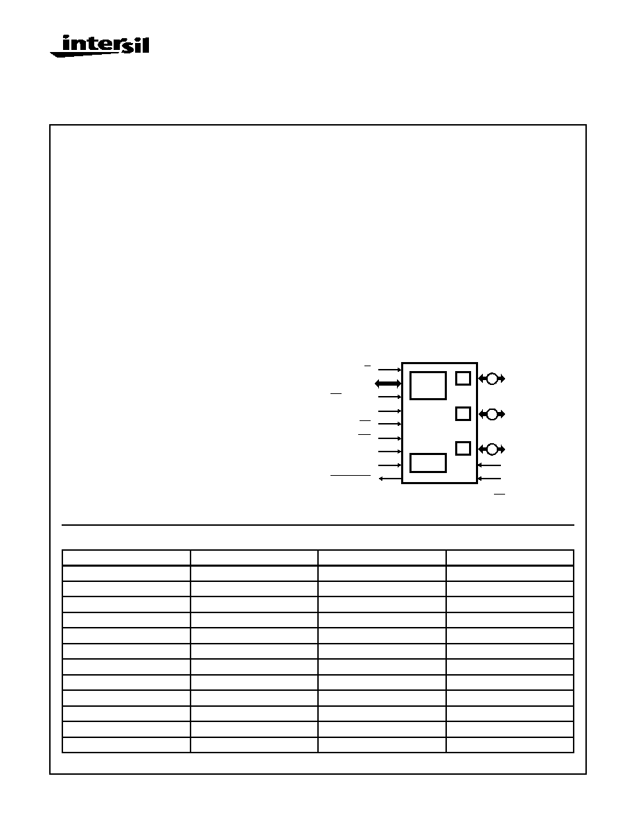
Functional Diagram
256 x 8
STATIC
RAM
A
B
C
TIMER
IO/M
AD0 - AD7
CE OR CE
ALE
RD
WR
RESET
TIMER CLK
TIMER OUT
8
PA0 - PA7
PORT A
8
PB0 - PB7
PORT B
8
PC0 - PC5
PORT C
VDD (10V)
GND
81C55RH = CE
81C56RH = CE
Ordering Information
PART NUMBER
TEMPERATURE RANGE
SCREENING LEVEL
PACKAGE
5962R9XXXX01QRC
-55
o
C to +125
o
C
MIL-PRF-38535 Level Q
40 Lead SBDIP
5962R9XXXX01VRC
-55
o
C to +125
o
C
MIL-PRF-38535 Level V
40 Lead SBDIP
5962R9XXXX01QXC
-55
o
C to +125
o
C
MIL-PRF-38535 Level Q
42 Lead Ceramic Flatpack
5962R9XXXX01VXC
-55
o
C to +125
o
C
MIL-PRF-38535 Level V
42 Lead Ceramic Flatpack
5962R9XXXX02QRC
-55
o
C to +125
o
C
MIL-PRF-38535 Level Q
40 Lead SBDIP
5962R9XXXX02VRC
-55
o
C to +125
o
C
MIL-PRF-38535 Level V
40 Lead SBDIP
5962R9XXXX02QXC
-55
o
C to +125
o
C
MIL-PRF-38535 Level Q
42 Lead Ceramic Flatpack
5962R9XXXX02VXC
-55
o
C to +125
o
C
MIL-PRF-38535 Level V
42 Lead Ceramic Flatpack
HS1-81C55RH/Sample
+25
o
C
Sample
40 Lead SBDIP
HS9-81C55RH/Sample
+25
o
C
Sample
42 Lead Ceramic Flatpack
HS1-81C56RH/Sample
+25
o
C
Sample
40 Lead SBDIP
HS9-81C56RH/Sample
+25
o
C
Sample
42 Lead Ceramic Flatpack
Spec Number
518056
File Number
3039.1
March 1996

2
HS-81C55RH, HS-81C56RH
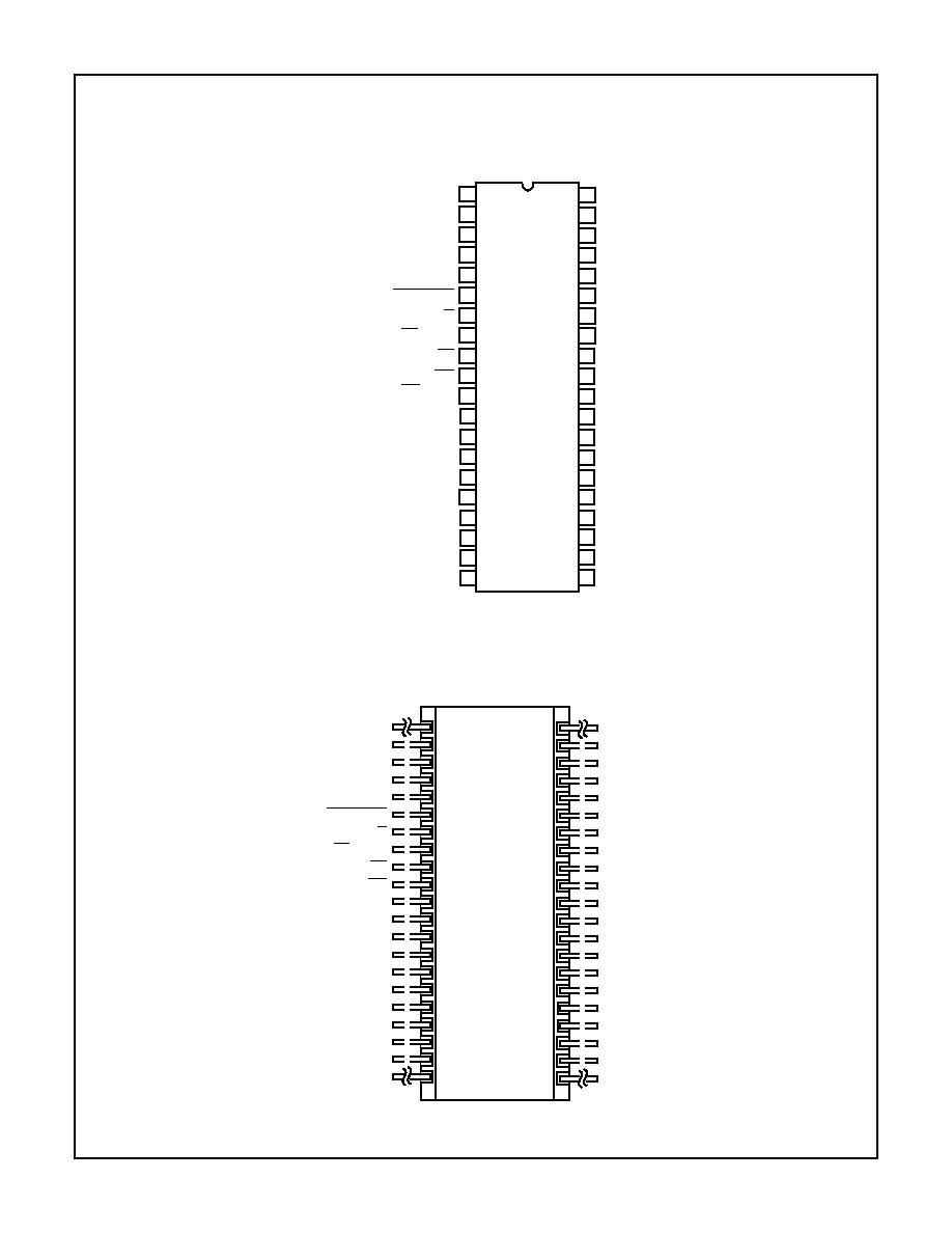
Pinouts
40 LEAD DUAL-IN-LINE METAL SEAL PACKAGE (SBDIP)
MIL-STD-1835 CDIP2-T40
TOP VIEW
42 LEAD CERAMIC METAL SEAL FLATPACK PACKAGE
INTERSIL OUTLINE K42.A
TOP VIEW
13
1
2
3
4
5
6
7
8
9
10
11
12
14
15
16
17
18
19
20
33
34
35
36
37
38
39
40
32
31
30
29
24
25
26
27
28
21
22
23
TIMER IN
RESET
GND
PC4
PC5
ALE
AD0
AD1
AD2
AD3
AD4
AD5
AD6
AD7
VDD
PC3
PC2
PC1
PC0
PB7
PB6
PB5
PB4
PB3
PB2
PB1
PB0
PA7
PA6
PA5
PA4
PA3
PA2
PA1
PA0
TIMER OUT
CE or CE*
WR
RD
IO / M
*81C55RH = CE
81C56RH = CE
PC1
PC2
PB6
PB1
PB2
VDD
PB4
PB0
PA7
PA6
PA5
NC
PA4
PA3
PA2
PA1
PC0
PA0
WR
ALE
RESET
PC5
TIMER OUT
IO/M
CE OR CE
RD
PC3
PC4
AD0
AD1
AD2
AD3
NC
AD6
AD7
GND
TIMER IN
AD4
AD5
PB3
PB5
PB7
33
32
39
38
37
36
35
34
42
41
31
30
29
28
27
24
23
22
40
26
25
10
11
4
5
6
7
8
9
1
2
12
13
14
15
16
19
20
21
3
17
18
Spec Number
518056

3
HS-81C55RH, HS-81C56RH
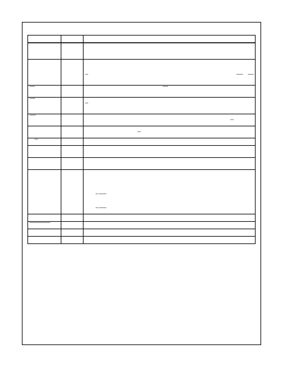
Pin Description
SYMBOL
TYPE
NAME AND FUNCTION
RESET
I
Reset: Pulse provided by the HS-80C85RH to initialize the system (connect to HS-80C85RH RESET
OUT). Input high on this line resets the chip and initializes the three I/O ports to input mode. The width
of RESET pulse should typically be two HS-80C85RH clock cycle times.
AD0 - AD7
I/O
Address/Data: Tri-state Address/Data lines that interface with the CPU lower 8-bit Address/Data Bus.
The 8-bit address is latched into the address latch inside the HS-81C55 and HS-81C56RH on the falling
edge of ALE. The address can be either for the memory section or the I/O section depending on the IO/
M input. The 8-bit data is either written into the chip or read from the chip, depending on the WR or RD
input signal.
CE or CE
I
Chip Enable: On the HS-81C55RH, this pin is CE and is ACTIVE LOW. On the HS-81C56RH, this pin
is CE and is ACTIVE HIGH.
RD
I
Read Control: Input low on this line with the Chip Enable active enables and AD0 - AD7 buffers. If IO/
M pin is low, the RAM content will be read out to the AD bus. Otherwise the content of the selected I/O
port or command/status registers will be read to the AD bus.
WR
I
Write Control: Input low on this line with the Chip Enable active causes the data on the Address/Data
bus to be written to the RAM or I/O ports and command/status register, depending on IO/M.
ALE
I
Address Latch Enable: This control signal latches both the address on the AD0 - AD7 lines and the
state of the Chip Enable and IO/M into the chip at the falling edge of ALE.
IO/M
I
I/O Memory: Selects memory if low and I/O and command/status registers if high.
PA0 - PA7 (8)
I/O
Port A: These 8 pins are general purpose I/O pins. The in/out direction is selected by programming the
command register.
PB0 - PB7 (8)
I/O
Port B: These 8 pins are general purpose I/O pins. The in/out direction is selected by programming the
command register.
PC0 - PC7 (8)
I/O
Port C: These 6 pins can function as either input port, output port, or as control signals for PA and PB.
Programming is done through the command register. When PC0 - PC5 are used as control signals, they
will provide the following:
PC0 - A INTR (Port A Interrupt)
PC1 - ABF (Port A Buffer Full)
PC2 - A STB (Port A Strobe)
PC3 - B INTR (Port B Interrupt)
PC4 - B BF (Port B Buffer Full)
PC5 - B STB (Port B Strobe)
TIMER IN
I
Timer Input: Input to the counter-timer.
TIMER OUT
O
Timer Output: This output can be either a square wave or a pulse, depending on the timer mode.
VDD
I
Voltage: +5V.
GND
I
Ground: Ground reference.
Spec Number
518056

4
Specifications HS-81C55RH, HS-81C56RH
Absolute Maximum Ratings
Reliability Information
Supply Voltage . . . . . . . . . . . . . . . . . . . . . . . . . . . . . . . . . . . . . +7.0V
Input, Output or I/O Voltage . . . . . . . . . . . . GND-0.3V to VDD+0.3V
Storage Temperature Range . . . . . . . . . . . . . . . . . -65
o
C to +150
o
C
Junction Temperature . . . . . . . . . . . . . . . . . . . . . . . . . . . . . . +175
o
C
Lead Temperature (Soldering 10s) . . . . . . . . . . . . . . . . . . . . +300
o
C
Typical Derating Factor . . . . . . . . . . . . 2mA/MHz Increase in IDDOP
ESD Classification . . . . . . . . . . . . . . . . . . . . . . . . . . . . . . . . Class 1
Thermal Resistance
JA
JC
SBDIP Package . . . . . . . . . . . . . . . . . . . .
40.0
o
C/W
5.0
o
C/W
Ceramic Flatpack Package . . . . . . . . . . .
45.0
o
C/W
5.0
o
C/W
Maximum Package Power Dissipation at +125
o
C
SBDIP Package . . . . . . . . . . . . . . . . . . . . . . . . . . . . . . . . . . 1.25W
Ceramic Flatpack Package . . . . . . . . . . . . . . . . . . . . . . . . . 1.11W
If device power exceeds package dissipation capability, provide heat
sinking or derate linearly at the following rate:
SBDIP Package . . . . . . . . . . . . . . . . . . . . . . . . . . . . . . 25.0mW/
o
C
Ceramic Flatpack Package . . . . . . . . . . . . . . . . . . . . . 22.2mW/
o
C
CAUTION: Stresses above those listed in "Absolute Maximum Ratings" may cause permanent damage to the device. This is a stress only rating and operation
of the device at these or any other conditions above those indicated in the operational sections of this specification is not implied.
Operating Conditions
Operating Voltage Range . . . . . . . . . . . . . . . . . . . +4.75V to +5.25V
Operating Temperature Range . . . . . . . . . . . . . . . . -55
o
C to +125
o
C
Input Low Voltage . . . . . . . . . . . . . . . . . . . . . . . . . . . . . .0V to +0.8V
Input High Voltage . . . . . . . . . . . . . . . . . . . . . . . . VDD -0.5V to VDD
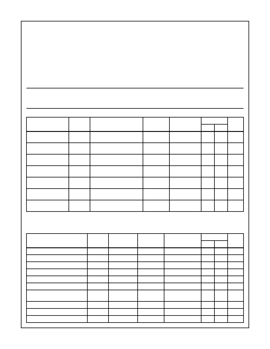
TABLE 1. DC ELECTRICAL PERFORMANCE CHARACTERISTICS
PARAMETERS
SYMBOL
CONDITIONS
GROUP A
SUBGROUPS
TEMPERATURE
LIMITS
UNITS
MIN
MAX
High Input Leakage
Current
IIH
VDD = 5.25V, VIN = 0V,
Pin under test = VDD
1, 2, 3
-55
o
C, +25
o
C,
+125
o
C
-
1
µ
A
Low Input Leakage
Current
IIL
VDD = 5.25V, VIN = 5.25V,
Pin under test = 0V
1, 2, 3
-55
o
C, +25
o
C,
+125
o
C
-1
-
µ
A
Low Output Voltage
VOL
VDD = 5.25V, IOL = 2mA
1, 2, 3
-55
o
C, +25
o
C,
+125
o
C
-
0.5
V
High Output Voltage
VOH
VDD = 4.75V, IOH = 2mA
1, 2, 3
-55
o
C, +25
o
C,
+125
o
C
4.25
-
V
Static Current
IDDSB
VDD = 5.25V
1, 2, 3
-55
o
C, +25
o
C,
+125
o
C
-
200
µ
A
Dynamic Current
IDDOP
VDD = 5.25V, f = 1MHz
1, 2, 3
-55
o
C, +25
o
C,
+125
o
C
-
2
mA
Functional Tests
FT
VDD = 4.75V and 5.25V,
VIH = VDD-0.5V, VIL = 0.8V
7, 8A, 8B
-55
o
C, +25
o
C,
+125
o
C
-
-
-
NOTE: All devices are guaranteed at worst case limits and over radiation. Dynamic current is proportional to operating frequency (2mA/MHz).
TABLE 2. AC ELECTRICAL PERFORMANCE CHARACTERISTICS
PARAMETERS
SYMBOL
CONDITIONS
GROUP A
SUBGROUPS
TEMPERATURE
LIMITS
UNITS
MIN
MAX
Address Latch Setup Time
TAL
Notes 1, 4
9, 10, 11
-55
o
C
T
A
+125
o
C
60
-
ns
Address Hold Time After Latch
TLA
Notes 1, 4
9, 10, 11
-55
o
C
T
A
+125
o
C
60
-
ns
Latch to READ/WRITE Control
TLC
Notes 1, 4
9, 10, 11
-55
o
C
T
A
+125
o
C
200
-
ns
Valid Data Out From Read Control
TRD
Notes 1, 4
9, 10, 11
-55
o
C
T
A
+125
o
C
-
250
ns
Address Stable to Data Out Valid
TAD
Notes 1, 4
9, 10, 11
-55
o
C
T
A
+125
o
C
-
500
ns
Latch Enable Width
TLL
Notes 1, 4
9, 10, 11
-55
o
C
T
A
+125
o
C
200
-
ns
READ/WRITE Control to Latch
Enable
TCL
Notes 1, 4,7
9, 10, 11
-55
o
C
T
A
+125
o
C
20
-
ns
READ/WRITE Control Width
TCC
Notes 1, 4
9, 10, 11
-55
o
C
T
A
+125
o
C
250
-
ns
Data In to WRITE Setup Time
TDW
Notes 1, 4
9, 10, 11
-55
o
C
T
A
+125
o
C
200
-
ns
Data In Hold Time After WRITE
TWD
Notes 1, 4
9, 10, 11
-55
o
C
T
A
+125
o
C
25
-
ns
Spec Number
518056

5
Specifications HS-81C55RH, HS-81C56RH
WRITE to Port Output
TWP
Notes 1, 4
9, 10, 11
-55
o
C
T
A
+125
o
C
-
300
ns
Port Input Setup Time
TPR
Notes 1, 4
9, 10, 11
-55
o
C
T
A
+125
o
C
50
-
ns
Port Input Hold Time
TRP
Notes 1, 4
9, 10, 11
-55
o
C
T
A
+125
o
C
15
-
ns
Strobe to Buffer Full
TSBF
Notes 1, 4
9, 10, 11
-55
o
C
T
A
+125
o
C
-
300
ns
Strobe Width
TSS
Notes 1, 4
9, 10, 11
-55
o
C
T
A
+125
o
C
150
-
ns
READ to Buffer Empty
TRBE
Notes 1, 4
9, 10, 11
-55
o
C
T
A
+125
o
C
-
300
ns
Strobe to INTR Off
TSI
Notes 1, 4
9, 10, 11
-55
o
C
T
A
+125
o
C
-
300
ns
READ to INTR Off
TRDI
Notes 1, 4
9, 10, 11
-55
o
C
T
A
+125
o
C
360
ns
Port Setup Time to Strobe
TPSS
Notes 1, 4, 5
9, 10, 11
-55
o
C
T
A
+125
o
C
100
-
ns
Post Hold Time After Strobe
TPHS
Notes 1, 4
9, 10, 11
-55
o
C
T
A
+125
o
C
100
-
ns
Strobe to Buffer Empty
TSBE
Notes 1, 4
9, 10, 11
-55
o
C
T
A
+125
o
C
-
300
ns
WRITE to Buffer full
TWBF
Notes 1, 4
9, 10, 11
-55
o
C
T
A
+125
o
C
-
300
ns
WRITE to INTR Off
TWI
Notes 1, 4
9, 10, 11
-55
o
C
T
A
+125
o
C
-
340
ns
TIMER-IN to TIMER OUT Low
TTL
Notes 1, 4
9, 10, 11
-55
o
C
T
A
+125
o
C
-
300
ns
TIMER-IN to TIMER-OUT High
TTH
Notes 1, 4
9, 10, 11
-55
o
C
T
A
+125
o
C
-
300
ns
Data Bus Enable from READ Control
TRDE
Notes 1, 4
9, 10, 11
-55
o
C
T
A
+125
o
C
120
-
ns
TIMER-IN Low Time
T1
Notes 1, 4, 6
9, 10, 11
-55
o
C
T
A
+125
o
C
40
-
ns
TIMER-IN High Time
T2
Notes 1, 4
9, 10, 11
-55
o
C
T
A
+125
o
C
115
-
ns
NOTES:
1. All devices guaranteed at worst case limits and over radiation.
2. Operating supply current (IDDOP) is proportional to operating frequency.
3. Output timings are measured with purely capacitive load.
4. For design purposes the limits are given as shown. For compatibility with the 80C85RH microprocessor, the AC parameters are tested
as maximums.
5. Parameter tested as part of the functional test. No read and record data available.
6. At low temperature, T1 is measured down to 10ns. If the reading is less than 10ns, the parameter will read 10ns.
7. Read and Record data available on failing data only.
TABLE 3. ELECTRICAL PERFORMANCE CHARACTERISTICS
PARAMETERS
SYMBOL
CONDITIONS
TEMPERATURE
LIMITS
UNITS
MIN
MAX
Input Capacitance
CIN
VDD = Open, f = 1MHz, All measurements
referenced to device ground
T
A
= +25
o
C
-
10
pF
I/O Capacitance
CI/O
VDD = Open, f = 1MHz, All measurements
referenced to device ground
T
A
= +25
o
C
-
12
pF
Output Capacitance
COUT
VDD = Open, f = 1MHz, All measurements
referenced to device ground
T
A
= +25
o
C
-
10
pF
Data Bus Float After
READ
TRDF
VDD = 4.75V
-55
o
C, +25
o
C,
+125
o
C
10
100
ns
Recovery Time Between
Controls
TRV
VDD = 4.75V
-55
o
C, +25
o
C,
+125
o
C
-
220
ns
NOTE: The parameters listed in Table 3 are controlled via design or process parameters and are not directly tested. These parameters are
characterized upon initial design release and upon design changes which would affect these characteristics.
TABLE 2. AC ELECTRICAL PERFORMANCE CHARACTERISTICS
(Continued)
PARAMETERS
SYMBOL
CONDITIONS
GROUP A
SUBGROUPS
TEMPERATURE
LIMITS
UNITS
MIN
MAX
Spec Number
518056
