 | –≠–ª–µ–∫—Ç—Ä–æ–Ω–Ω—ã–π –∫–æ–º–ø–æ–Ω–µ–Ω—Ç: 82C237 | –°–∫–∞—á–∞—Ç—å:  PDF PDF  ZIP ZIP |
4-148
March 1997
82C237
CMOS High Performance
Programmable DMA Controller
Features
∑ Fully Compatible with Intersil 82C37A
- 82C237 May be Used in 8MHz and 12.5MHz 82C37A
Sockets
∑ Optimized for 10MHz and 12.5MHz 80C286 Systems
∑ Special Mode Permits 16-Bit, Zero Wait State DMA
Transfers
∑ High Speed Data Transfers:
- Up to 6.25MBytes/sec with 12.5MHz Clock in
Normal Mode
- Up to 12.5MBytes/sec with 12.5MHz Clock in 16-Bit
Mode
∑ Compatible with the NMOS 8237A
∑ Four Independent Maskable Channels with Autoinitial-
ization Capability
∑ Cascadable to any Number of Channels
∑ Memory-to-Memory Transfers
∑ Static CMOS Design Permits Low Power Operation
- ICCSB = 10
µ
A Maximum
- ICCOP = 2mA/MHz Maximum
∑ Fully TTL/CMOS Compatible
∑ Internal Registers may be Read from Software
Description
The 82C237 is a modified version of the 82C37A. The
82C237 is fully software and pin for pin compatible with the
82C37A but provides an additional mode for 16-bit DMA
transfers, as well as enhanced speed. Each channel may be
individually programmed for 8-bit or 16-bit data transfers.
The 82C237 controller can improve system performance by
allowing external devices to transfer data directly to or from
system memory. Memory-to-memory transfer capability is
also provided, along with a memory block initialization fea-
ture. DMA requests may be generated by either hardware or
software, and each channel is independently programmable
with a variety of features for flexible operation.
The 82C237 is designed to be used with an external address
latch, such as the 82C82, to demultiplex the most significant
8 bits of address. An additional latch is required to
temporarily store the most significant 8 bits of data if 16-bit
memory-to-memory transfers are desired. The 82C237 can
be used with industry standard microprocessors such as
80C286, 80286, 80C86, 80C88, 8086, 8088, 8085, Z80,
NSC800, 80186 and others. Multimode programmability
allows the user to select from three basic types of DMA
services, and reconfiguration under program control is
possible even with the clock to the controller stopped. Each
channel has a full 64K address and word count range, and
may be programmed to autoinitialize these registers
following DMA termination (end of process).
Ordering Information
PACKAGE
TEMPERATURE
RANGE
8MHz
12.5MHz
PKG. NO.
PDIP
0
o
C to +70
o
C
CP82C237
CP82C237-12
E40.6
-40
o
C to +85
o
C
IP82C237
IP82C237-12
E40.6
PLCC
0
o
C to +70
o
C
CS82C237
CS82C237-12
N44.65
-40
o
C to +85
o
C
IS82C237
IS82C237-12
N44.65
SBDIP
0
o
C to +70
o
C
CD82C237
CD82C237-12
F40.6
-40
o
C to +85
o
C
ID82C237
ID82C237-12
F40.6
-55
o
C to +125
o
C
MD82C237/B
MD82C237-12/B
F40.6
SMD#
5962-9054304MQA
5962-9054305MQA
F40.6
CLCC
-55
o
C to +125
o
C
MR82C237/B
MR82C237-12/B
J44.A
SMD#
5962-9054304MXA
5962-9054305MXA
J44.A
File Number
2965.1
CAUTION: These devices are sensitive to electrostatic discharge; follow proper IC Handling Procedures.
http://www.intersil.com or 407-727-9207
|
Copyright
©
Intersil Corporation 1999
4-149
82C237
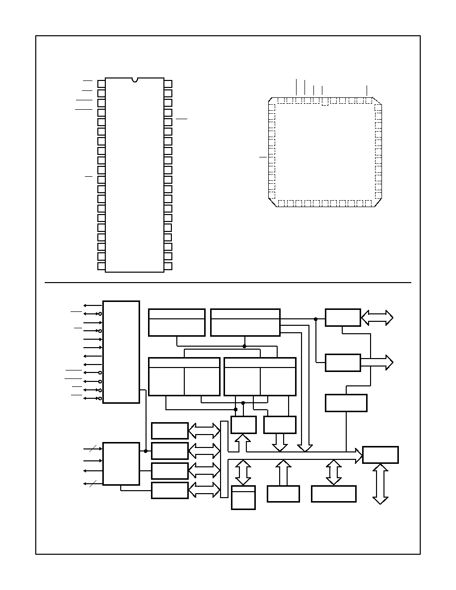
Block Diagram
Pinouts
82C237 (DIP)
TOP VIEW
82C237 (CLCC/PLCC)
TOP VIEW
13
1
2
3
4
5
6
7
8
9
10
11
12
14
15
16
17
18
19
20
IOR
IOW
MEMR
MEMW
DWLE
READY
HLDA
ADSTB
AEN
HRQ
CS
CLK
RESET
DACK2
DACK3
DREQ3
DREQ2
DREQ1
DREQ0
(GND) VSS
28
40
39
38
37
36
35
34
33
32
31
30
29
27
26
25
24
23
22
21
A7
A6
A5
A4
EOP
A3
A2
A1
A0
V
CC
DB0
DB1
DB2
DB3
DB4
DACK0
DACK1
DB5
DB6
DB7
(NOTE)
14
13
12
11
10
9
8
7
17
16
15
2
5
30
35
39
38
37
36
33
34
32
31
29
4
6
3
1
40
41
42
43
44
28
27
26
25
24
23
22
21
20
19
18
CS
DACK2
NC
NC
CLK
HRQ
NC
A3
A2
A1
A0
V
CC
DB0
DB1
DB2
DB3
NC
DB4
READ
Y
D
WLE
A7
A6
A5
MEMW
A4
EOP
D
A
CK3
DREQ3
DREQ2
DREQ1
DREQ0
GND
DB5
D
A
CK1
DB7
D
A
CK0
DB6
MEMR
ADSTB
AEN
IO
W
RESET
HLDA
IOR
NOTE: See Pin Description.
(NO
TE)
A4 - A7
EOP
RESET
CS
READY
CLK
AEN
ADSTB
MEMR
MEMW
IOR
IOW
TIMING
AND
CONTROL
DREQ0 -
HLDA
HRQ
DACK0 -
PRIORITY
ENCODER
AND
ROTATING
PRIORITY
LOGIC
DACK3
4
DREQ3
4
COMMAND
(8)
MASK
(4)
REQUEST
(4)
MODE
(4 x 6)
STATUS
(8)
TEMPORARY
(8)
INTERNAL DATA BUS
DECREMENTOR
COUNT REG (16)
TEMP WORD
INC DECREMENTOR
REG (16)
TEMP ADDRESS
BUFFER
IO
16-BIT BUS
READ BUFFER
ADDRESS
BASE
(16)
WORD
BASE
COUNT
(16)
READ WRITE BUFFER
ADDRESS
CURRENT
(16)
WORD
CURRENT
COUNT
(16)
16-BIT BUS
BUFFER
WRITE
BUFFER
READ
A8 - A15
BUFFER
OUTPUT
CONTROL
COMMAND
D0 - D1
A0 - A3
BUFFER
IO
DB0 - DB7
DWLE
DATA-WIDTH
(4)
4-150
82C237
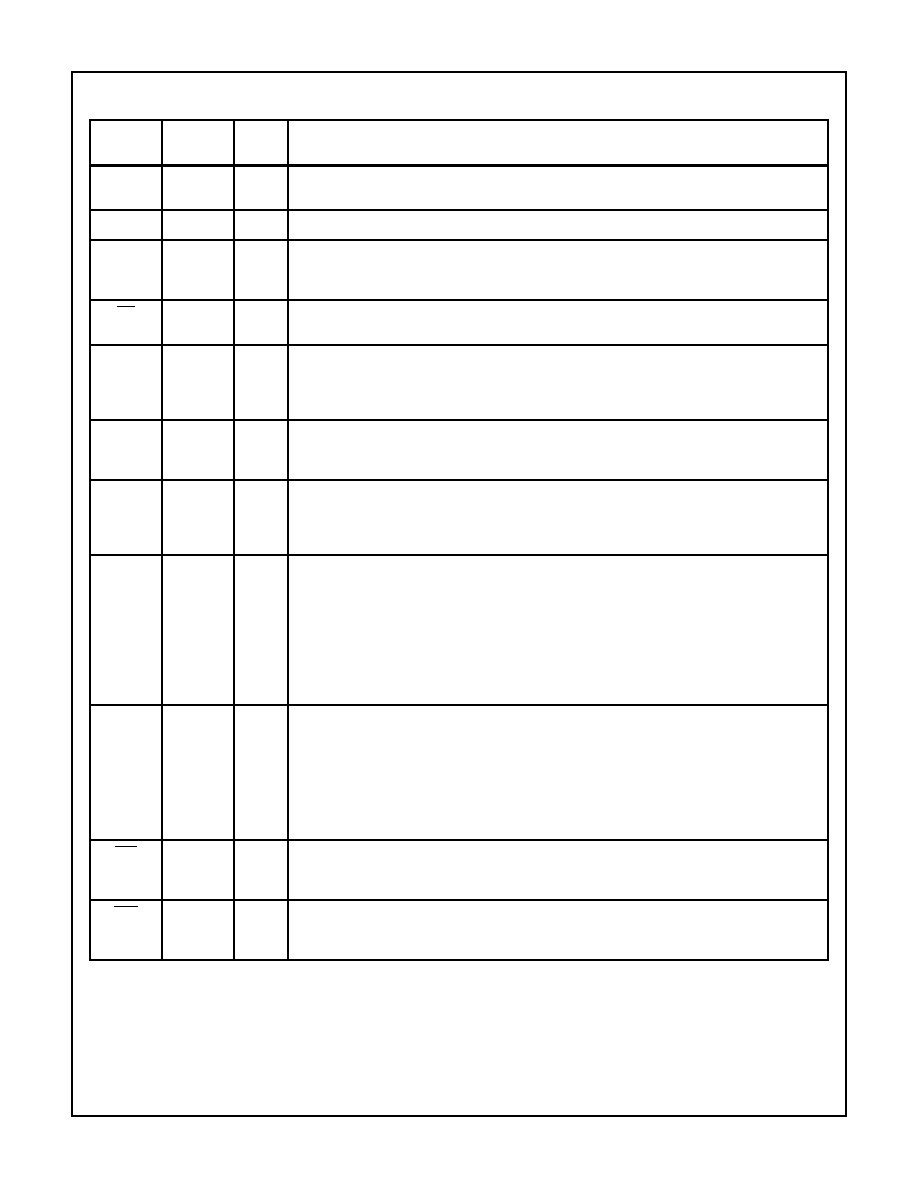
Pin Description
SYMBOL
PIN
NUMBER
TYPE
DESCRIPTION
V
CC
31
V
CC
: is the +5V power supply pin. A 0.1
µ
F capacitor between pins 31 and 20 is recommended for
decoupling.
GND
20
Ground
CLK
12
I
CLOCK INPUT: The Clock Input is used to generate the timing signals which control 82C237
operations. This input may be driven from DC to 12.5MHz for the 82C237-12 or from DC to 8MHz
for the 82C237. The Clock may be stopped in either state for standby operation.
CS
11
I
CHIP SELECT: Chip Select is an active low input used to enable the controller onto the data bus for
CPU communications.
RESET
13
I
RESET: This is an active high input which clears the Command, Status, Request, and Temporary
registers, the First/Last Flip-Flop, and the mode register counter. The Mask register is set to ignore
requests. The Data-Width register is set to perform 8-bit transfers on all channels (82C237 only).
Following a Reset, the controller is in an idle cycle.
READY
6
I
READY: This signal can be used to extend the memory read and write pulses from the 82C237 to
accommodate slow memories or I/O devices. READY must not make transitions during its specified
set-up and hold times. See Figure 14 for timing. READY is ignored in verify transfer mode.
HLDA
7
I
HOLD ACKNOWLEDGE: The active high Hold Acknowledge from the CPU indicates that it has
relinquished control of the system busses. HLDA is a synchronous input and must not transition
during its specified set-up time. There is an implied hold time (HLDA inactive) of TCH from the rising
edge of clock, during which time HLDA must not transition.
DREQ0-
DREQ3
16-19
I
DMA REQUEST: The DMA Request (DREQ) lines are individual asynchronous channel request
inputs used by peripheral circuits to obtain DMA service. In Fixed Priority, DREQ0 has the highest
priority and DREQ3 has the lowest priority. A request is generated by activating the DREQ line of a
channel. DACK will acknowledge the recognition of a DREQ signal. Polarity of DREQ is
programmable. RESET initializes these lines to active high. DREQ must be maintained until the
corresponding DACK goes active. DREQ will not be recognized while the clock is stopped. Unused
DREQ inputs should be pulled High or Low (inactive) and the corresponding mask bit set. In 16-bit
Transfer mode (82C237 only), each DREQ channel may be programmed to perform either 8-bit or
16-bit DMA transfers.
DB0-DB7
21-23
26-30
I/O
DATA BUS: The Data Bus lines are bidirectional three-state signals connected to the system data
bus. The outputs are enabled in the Program condition during the I/O Read to output the contents
of a register to the CPU. The outputs are disabled and the inputs are read during an I/O Write cycle
when the CPU is programming the 82C237 control registers. During DMA cycles, the most signifi-
cant 8-bits of the address are output onto the data bus to be strobed into an external latch by ADSTB.
In memory-to-memory operations, data from the memory enters the 82C237 on the data bus during
the read-from-memory transfer, then during the write-to-memory transfer, the data bus outputs write
the data into the new memory location.
IOR
1
I/O
I/O READ: I/O Read is a bidirectional active low three-state line. In the Idle cycle, it is an input con-
trol signal used by the CPU to read the control registers. In the Active cycle, it is an output control
signal used by the 82C237 to access data from the peripheral during a DMA Write transfer.
IOW
2
I/O
I/O WRITE: I/O Write is a bidirectional active low three-state line. In the Idle cycle, it is an input con-
trol signal used by the CPU to load information into the 82C237. In the Active cycle, it is an output
control signal used by the 82C237 to load data to the peripheral during a DMA Read transfer.
4-151
82C237
EOP
36
I/O
END OF PROCESS: End of Process (EOP) is an active low bidirectional signal. Information
concerning the completion of DMA services is available at the bidirectional EOP pin.
The 82C237 allows an external signal to terminate an active DMA service by pulling the EOP pin
low. A pulse is generated by the 82C237 when terminal count (TC) for any channel is reached,
except for channel 0 in memory-to-memory mode. During memory-to-memory transfers, EOP will
be output when the TC for channel 1 occurs.
The EOP pin is driven by an open drain transistor on-chip, and requires an external pull-up resistor
to V
CC
.
When an EOP pulse occurs, whether internally or externally generated, the 82C237 will terminate
the service, and if autoinitialize is enabled, the base registers will be written to the current registers
of that channel. The mask bit and TC bit in the status word will be set for the currently active channel
by EOP unless the channel is programmed for autoinitialize. In that case, the mask bit remains clear.
A0-A3
32-35
I/O
ADDRESS: The four least significant address lines are bidirectional three-state signals. In the Idle
cycle, they are inputs and are used by the 82C237 to address the control register to be loaded or
read. In the Active cycle, they are outputs and provide the lower 4-bits of the output address. When
in 16-bit mode (82C237 only), and the active channel is a 16-bit channel (as defined by the Data-
Width register), then A0 will remain low during the entire transfer (i.e. an even word address will al-
ways be generated).
A4-A7
37-40
O
ADDRESS: The four most significant address lines are three-state outputs and provide 4-bits of
address. These lines are enabled only during the DMA service.
HRQ
10
O
HOLD REQUEST: The Hold Request (HRQ) output is used to request control of the system bus.
When a DREQ occurs and the corresponding mask bit is clear, or a software DMA request is made,
the 82C237 issues HRQ. The HLDA signal then informs the controller when access to the system
busses is permitted. For stand-alone operation where the 82C237 always controls the busses, HRQ
may be tied to HLDA. This will result in one S0 state before the transfer.
DACK0-
DACK3
14, 15
24, 25
O
DMA ACKNOWLEDGE: DMA acknowledge is used to notify the individual peripherals when one
has been granted a DMA cycle. The sense of these lines is programmable. RESET initializes them
to active low.
AEN
9
O
ADDRESS ENABLE: Address Enable enables the 8-bit latch containing the upper 8 address bits
onto the system address bus. AEN can also be used to disable other system bus drivers during DMA
transfers. AEN is active HIGH.
ADSTB
8
O
ADDRESS STROBE: This is an active high signal used to control latching of the upper address
byte. It will drive directly the strobe input of external transparent octal latches, such as the 82C82.
During block operations, ADSTB will only be issued when the upper address byte must be updated,
thus speeding operation through elimination of S1 states. ADSTB timing is referenced to the falling
edge of the 82C237 clock.
MEMR
3
O
MEMORY READ: The Memory Read signal is an active low three-state output used to access data
from the selected memory location during a DMA Read or a memory-to-memory transfer.
MEMW
4
O
MEMORY WRITE: The Memory Write is an active low three-state output used to write data to the
selected memory location during a DMA Write or a memory-to-memory transfer.
DWLE
5
O
DATA-WIDTH, LATCH ENABLE: In normal 8-bit transfer mode (16-bit transfer mode not enabled),
this output is always high impedance three-stated. In 16-bit transfer mode (82C237 only), this output
serves a dual purpose. During S1 cycles, the DWLE output indicates the data width (0 = 16-bit, 1 =
8-bit) of the active channel. During memory-to-memory transfers, the DWLE output is used to enable
an external latch which temporarily stores the 8 most significant bits of data during the read-from-
memory transfer. DWLE enables this byte of data onto the data bus during the write-to-memory
transfer of a memory-to-memory operation.
Pin Description
(Continued)
SYMBOL
PIN
NUMBER
TYPE
DESCRIPTION
4-152
82C237
Functional Description
The 82C237 is an improved version of the Intersil 82C37A
DMA controller and is fully software and pin for pin compati-
ble with the 82C37A. All operational and pin descriptions of
the 82C37A apply to the 82C237 with additional features
noted in the section titled 82C237 Operation.
The 82C237 direct memory access controller is designed to
improve the data transfer rate in systems which must
transfer data from an I/O device to memory, or move a block
of memory to an I/O device. It will also perform memory-to-
memory block moves, or fill a block of memory with data
from a single location. Operating modes are provided to
handle single byte transfers as well as discontinuous data
streams, which allows the 82C237 to control data movement
with software transparency.
The DMA controller is a state-driven address and control
signal generator, which permits data to be transferred
directly from an I/O device to memory or vice versa without
ever being stored in a temporary register. This can greatly
increase the data transfer rate for sequential operations,
compared with processor move or repeated string
instructions. Memory-to-memory operations require
temporary internal storage of the data byte between
generation of the source and destination addresses, so
memory-to-memory transfers take place at less than half the
rate of I/O operations, but still much faster than with central
processor techniques. The maximum data transfer rates
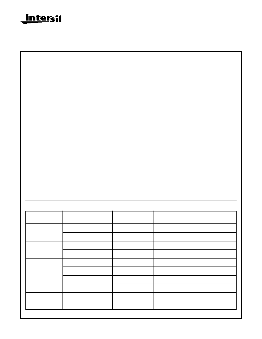
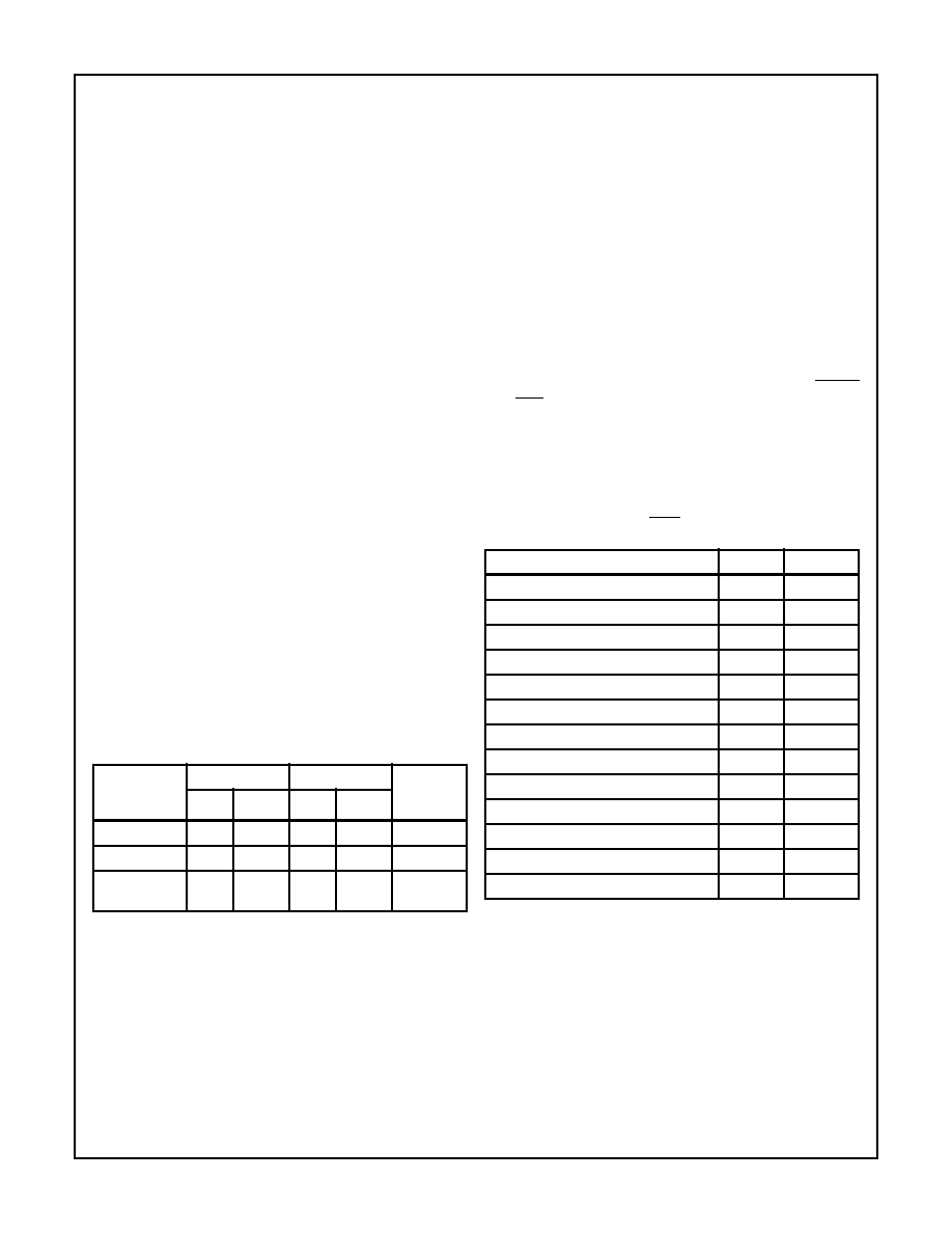
obtainable with the 82C237 are shown in Figure 1.
The block diagram of the 82C237 is shown on page 2. The
timing and control block, priority block, and internal registers
are the main components. Figure 2 lists the name and size
of the internal registers. The timing and control block derives
internal timing from CLK input, and generates external
control signals. The Priority Encoder block resolves priority
contention between DMA channels requesting service
simultaneously.
DMA Operation
In a system, the 82C237 address and control outputs and
data bus pins are basically connected in parallel with the
system busses. An external latch is required for the upper
address byte. While inactive, the controller's outputs are in a
high impedance state. When activated by a DMA request
and bus control is relinquished by the host, the 82C237
drives the busses and generates the control signals to
perform the data transfer. The operation performed by
activating one of the four DMA request inputs has previously
been programmed into the controller via the Command,
Mode, Address, and Word Count registers.
For example, if a block of data is to be transferred from RAM
to an I/O device, the starting address of the data is loaded
into the 82C237 Current and Base Address registers for a
particular channel, and the length of the block is loaded into
the channel's Word Count register. The corresponding Mode
register is programmed for a memory-to-I/O operation (read
transfer), and various options are selected by the Command
register and the other Mode register bits. The channel's
mask bit is cleared to enable recognition of a DMA request
(DREQ). The DREQ can either be a hardware signal or a
software command.
Once initiated, the block DMA transfer will proceed as the
controller outputs the data address, simultaneous MEMR
and IOW pulses, and selects an I/O device via the DMA
acknowledge (DACK) outputs. The data byte flows directly
from the RAM to the I/O device. After each byte is
transferred, the address is automatically incremented (or
decremented) and the word count is decremented. The
operation is then repeated for the next byte. The controller
stops transferring data when the Word Count register
underflows, or an external EOP is applied.
To further understand 82C237 operation, the states
generated by each CLK cycle must be considered. The DMA
controller operates in two major cycles, active and idle. After
being programmed, the controller is normally idle until a
DMA request occurs on an unmasked channel, or a software
request is given. The 82C237 will then request control of the
system busses and enter the active cycle. The active cycle is
composed of several internal states, depending on what
options have been selected and what type of operation has
been requested.
82C237
TRANSFER
TYPE
8MHz
12.5MHz
UNIT
8-BIT
16-BIT
8-BIT
16-BIT
Compressed
4.00
8.00
6.25
12.5
MByte/sec
Normal I/O
2.67
5.34
4.17
8.34
MByte/sec
Memory-to-
Memory
1.00
2.00
1.56
3.12
MByte/sec
FIGURE 1. DMA TRANSFER RATES
NAME
SIZE
NUMBER
Base Address Registers
16-Bits
4
Base Word Count Registers
16-Bits
4
Current Address Registers
16-Bits
4
Current Word Count Registers
16-Bits
4
Temporary Address Register
16-Bits
1
Temporary Word Count Register
16-Bits
1
Status Register
8-Bits
1
Command Register
8-Bits
1
Temporary Register
8-Bits
1
Mode Registers
6-Bits
4
Mask Register
4-Bits
1
Request Register
4-Bits
1
Data-Width Register (See Note)
4-Bits
1
NOTE: 82C237 only
FIGURE 2. 82C237 INTERNAL REGISTERS