 | –≠–ª–µ–∫—Ç—Ä–æ–Ω–Ω—ã–π –∫–æ–º–ø–æ–Ω–µ–Ω—Ç: 82C284-12 | –°–∫–∞—á–∞—Ç—å:  PDF PDF  ZIP ZIP |

1
TM
March 1997
82C284
Clock Generator and Ready Interface
for 80C286 Processors
Features
∑ Generates System Clock for 80C286 Processors
∑ Generates System Reset Output from Schmitt
Trigger Input
- Improved Hysteresis
∑ Uses Crystal or External Signal for Frequency Source
∑ Dynamically Switchable between Two Input
Frequencies
∑ Provides Local READY and MULTIBUS
READY
Synchronization
∑ Static CMOS Technology
∑ Single +5V Power Supply
∑ Available in 18 Lead CerDIP Package
Description
The Intersil 82C284 is a clock generator/driver which pro-
vides clock signals for 80C286 processors and support com-
ponents. It also contains logic to supply READY to the CPU
from either asynchronous or synchronous sources and syn-
chronous RESET from an asynchronous input with hystere-
sis.
Pinout
82C284 (CERDIP)
TOP VIEW
Functional Diagram
Ordering Information
PART NUMBER
TEMP. RANGE
PACKAGE
PKG.
NO.
CD82C284-12
0
o
C to +70
o
C
18 Ld CERDIP F18.3
ID82C284-10
-40
o
C to +85
o
C
18 Ld CERDIP F18.3
ID82C284-12
-40
o
C to +85
o
C
18 Ld CERDIP F18.3
10
11
12
13
14
15
16
17
18
9
8
7
6
5
4
3
2
1
VCC
S1
S0
NC
PCLK
RESET
RES
ARDYEN
CLK
ARDY
SRDY
SRDYEN
READY
EFI
F/C
X2
X1
GND
RESET
SYNCHRONIZER
RES
X1
X2
EFI
F/C
ARDYEN
ARDY
SRDYEN
SRDY
S1
S0
RESET
CLK
READY
PCLK
XTAL
OSC
MUX
SYNCHRONIZER
READY LOGIC
PCLK GENERATOR
CAUTION: These devices are sensitive to electrostatic discharge; follow proper IC Handling Procedures.
1-888-INTERSIL or 321-724-7143
|
Intersil (and design) is a trademark of Intersil Americas Inc.
Copyright © Intersil Americas Inc. 2002. All Rights Reserved
MULTIBUS
is a patented Intel bus.
FN2966.1

2
Pin Description
The following pin function descriptions are for the 82C284 clock generator.
PIN
SYMBOL
NUMBER
TYPE
DESCRIPTION
CLK
10
O
SYSTEM CLOCK: the signal used by the processor and support devices which must be synchro-
nous with the processor. The frequency of the CLK output has twice the desired internal processor
clock frequency. CLK can drive both TTL and CMOS level inputs.
F/C
6
I
FREQUENCY/CRYSTAL SELECT: this pin selects the source for the CLK output. When there is a
LOW level on this input, the internal crystal oscillator drives CLK. When there is a HIGH level on F/C,
the EFI input drives the CLK input. This pin can be dynamically switched, which allows changing the
processor CLK frequency while running for low-power operation, etc.
X1, X2
7, 8
I
CRYSTAL IN: the pin stop which parallel resonant, fundamental mode crystal is attached for the in-
ternal oscillator. When F/C is LOW, the internal oscillator will drive the CLK output at the crystal fre-
quency. The crystal frequency must be twice the desired internal processor clock frequency.
EFI
5
I
EXTERNAL FREQUENCY IN: drives CLK when the F/C input is HIGH. The EFI input frequency must
be twice the desired internal processor clock frequency.
PCLK
13
O
PERIPHERAL CLOCK: the output which provides a 50% duty cycle clock with one-half the frequen-
cy of CLK. PCLK will be in phase with the internal processor clock following the first bus cycle after
the processor has been reset.
ARDYEN
17
I
ASYNCHRONOUS READY ENABLE: an active LOW input which qualifies the ARDY input.
ARDYEN selects ARDY as the source of READY for the current bus cycle. Inputs to ARDYEN may
be applied asynchronously to CLK. Setup and hold times are given to assure a guaranteed response
to synchronous outputs.
ARDY
1
I
ASYNCHRONOUS READY: an active LOW input used to terminate the current bus cycle. The
ARDY input is qualified by ARDYEN. Inputs to ARDY may be applied asynchronously to CLK. Setup
and hold times are given to assure a guaranteed response to synchronous outputs.
SRDYEN
3
I
SYNCHRONOUS READY ENABLE: an active LOW input which qualifies SRDY. SRDYEN selects
SRDY as the source for READY to the CPU for the current bus cycle. Setup and hold time must be
satisfied for proper operation.
SRDY
2
I
SYNCHRONOUS READY: an active LOW input used to terminate the current bus cycle. The SRDY
input is qualified by the SRDYEN input. Setup and hold time must be satisfied for proper operation.
READY
4
O
READY: an active LOW output which signals to the processor that the current bus cycle is to be com-
pleted. The SRDY SRDYEN, ARDY, ARDYEN, S1, S0, and RES inputs control READY as explained
later in the READY generator section. READY is an open drain output requiring an external pull-up
resistor.
S0, S1
15,16
I
STATUS: these inputs prepare the 82C284 for a subsequent bus cycle. S0 and S1 synchronize
PCLK to the internal processor clock and control READY. Setup and hold times must be satisfied for
proper operation
RESET
12
O
RESET: an active HIGH output which is derived from the RES input RESET is used to force the sys-
tem into an initial state. When RESET is active, READY will be active (LOW).
RES
11
I
RESET IN: an active LOW input which generates the system reset signal (RESET). Signals to RES
may be applied asynchronously to CLK. A Schmitt trigger input is provided on RES, so that an RC
circuit can be used to provide a time delay. Setup and hold times are given to assure a guaranteed
response to synchronous inputs.
V
CC
18
SYSTEM POWER: The +5V Power Supply Pin. A 0.1
µ
F capacitor between V
CC
and GND is recom-
mended for decoupling.
GND
9
SYSTEM GROUND: 0V
82C284

3
Functional Description
Introduction
The 82C284 generates the clock, ready, and reset signals
required for 80C286 processors and support components.
The 82C284 is packaged in an 18-pin DIP and contains a
crystal controlled oscillator, clock generator, peripheral clock
generator, MULTIBUSÆ ready synchronization logic, and
system reset generation logic.
Clock Generator
The CLK output provides the basic timing control for an
80C286 system. CLK has output characteristics sufficient to
drive CMOS devices. CLK is generated by either an internal
crystal oscillator, or an external source as selected by the
F/C input pin. When F/C is LOW, the crystal oscillator drives
the CLK output. When F/C is HIGH, the EFI input drives the
CLK output.
The F/C pin on the Intersil 82C284 is dynamically switch-
able. This allows the CLK frequency to the processor to be
changed from one frequency to another in a running system.
With this feature, a system can be designed which operates
at maximum speed when needed, and then dynamically
switched to a lower frequency to implement a low-power
mode. The lower frequency can be anything down to, but
excluding, DC. The following 3 conditions apply when
dynamically switching the F/C pin (see Figure 1):
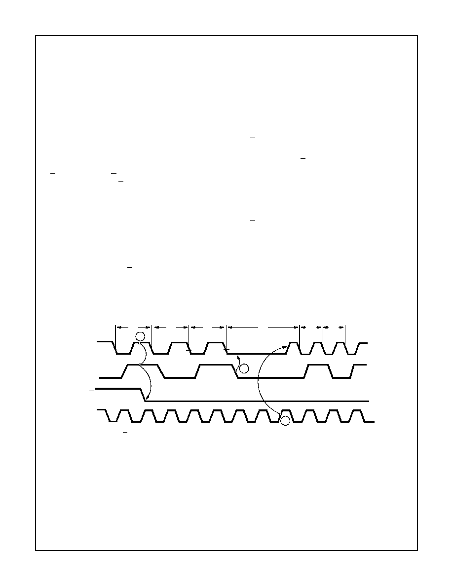
1) The CLK is stretched in the low portion of the
2 phase
of its cycle during transition from one CLK frequency to
the other (see Waveforms).
2) When switching CLK frequency sources, there is a max-
imum transition latency of 2.5 clock cycles of the fre-
quency being switched to, from the time CLK freezes
low, until CLK restarts at the new frequency (see Wave-
forms).
3) The maximum latency from the time F/C is dynamically
switched, to the time CLK freezes low, is 4 CLK cycles
(see Waveforms).
The following steps describe the sequence of events that
transpire when F/C is dynamically switched:
A) F/C switched from high (using EFI input) to low (using
the crystal input X1 - see Figure 1A).
1) The state of F/C is sampled when both CLK and
PCLK are high until a change is detected.
2) On the second following falling edge of PCLK, CLK is
frozen low.
3) CLK restarts at the crystal frequency on the rising
edge of Xl, after the second falling edge of X1.
B) F/C switched from low (using the crystal input Xl) to high
(using the EFI input - see Figure 1B).
1) The state of F/C is sampled when both CLK and
PCLK are high until a change is detected.
2) On the second following falling edge of PCLK, CLK is
frozen low.
3) CLK restarts at the EFI input frequency on the falling
edge of EFl after the second rising edge of EFI.
FIGURE 1A. F/C SWITCHED FROM HIGH (USING EFI INPUT) TO LOW (USING THE CRYSTAL INPUT X1)
2
1
2
1
2
1
1
2
3
CLK
PCLK
F/C
X1
82C284

4
The 82C284 provides a second clock output, PCLK, for periph-
eral devices. PCLK is CLK divided by two. PCLK has a duty
cycle of 50% and CMOS output drive characteristics. PCLK is
normally synchronized to the internal processor clock.
After reset, the PCLK signal may be out of phase with the inter-
nal processor clock. The S1 and S0 signals of the first bus
cycle are used to synchronize PCLK to the internal processor
clock. The phase of the PCLK output changes by extending its
HIGH time beyond one system clock (see waveforms). PCLK is
forced HIGH whenever either S0 or S1 were active (LOW) for
the two previous CLK cycles. PCLK continues to oscillate when
both S0 and S1 are HIGH.
Since the phase of the internal processor clock will not change
except during reset, the phase of PCLK will not change except
during the first bus cycle after reset.
Oscillator
The oscillator circuit of the 82C284 is a linear Pierce oscillator
which requires an external parallel resonant, fundamental
mode, crystal. The output of the oscillator is internally buffered.
The crystal frequency chosen should be twice the required
internal processor clock frequency. The crystal should have a
typical load capacitance of 32pF.
X1 and X2 are the oscillator crystal connections. For stable
operation of the oscillator, two loading capacitors are recom-
mended, as shown in Table 1. The sum of the board capaci-
tance and loading capacitance should equal the values shown.
It is advisable to limit stray board capacitances (not including
the effect of the loading capacitors or crystal capacitance) to
less than 10pF between the X1 and X2 pins. Decouple V
CC
and GND as close to the 82C284 as possible with a 0.1
µ
F poly-
carbonate capacitor.
CLK Termination
Due to the CLK output having a very fast rise and fall time, it is
recommended to properly terminate the CLK line at frequen-
cies above 10MHz to avoid signal reflections and ringing. Ter-
mination is accomplished by inserting a small resistor
(typically 10-74
) in series with the output, as shown in Figure
2. This is known as series termination. The resistor value plus
the circuit output impedance (approximately 25
) should be
made equal to the impedance of the transmission line.
Reset Operation
The reset logic provides the RESET output to force the sys-
tem into a known, initial state. When the RES input is active
(LOW), the RESET output becomes active (HIGH), RES is
synchronized internally at the falling edge of CLK before
generating the RESET output (see waveforms). Synchroni-
zation of the RES input introduces a one or two CLK delay
before affecting the RESET Output.
At power up, a system does not have a stable V
CC
and CLK.
To prevent spurious activity, RES should be asserted until
V
CC
and CLK stabilize at their operating values. 80C286
processors and support components also require their
RESET inputs be HIGH a minimum of 16 CLK cycles. An RC
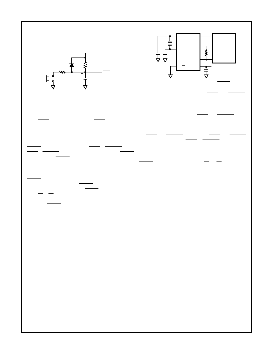
network, as shown in Figure 3, will keep RES LOW long
enough to satisfy both needs.
A Schmitt trigger input with hysteresis on RES assures a single
transition of RESET with an RC circuit on RES. The hysteresis
separates the input voltage level at which the circuit output
switches from HIGH to LOW from the input voltage level at
which the circuit output switches from LOW to HIGH. The RES
HIGH to LOW input transition voltage is lower than the RES
FIGURE 1B. F/C SWITCHED FROM LOW (USING THE CRYSTAL INPUT X1) TO HIGH (USING THE EFI INPUT)
FIGURE 1. DYNAMICALLY SWITCHING THE F/C PIN
CLK
PCLK
F/C
EFI
1
2
1
2
1
2
2
3
1
TABLE 1. 82C284 CRYSTAL LOADING CAPACITANCE VALUES
CRYSTAL
FREQUENCY
Cl
CAPACITANCE
(PIN 7)
C2
CAPACITANCE
(PIN 8)
1MHz to 8MHz
60pF
40pF
8MHz to 20MHz
25pF
15pF
20MHz to 25MHz
15pF
15pF
CLK
OUT
CLOSELY
PLACED
LOADS
CLOSELY
PLACED
LOADS
R
TRANSMISSION
LINE
RO
25
FIGURE 2. SERIES TERMINATION
Z
Z
82C284

5
LOW to HIGH input transition voltage. As long as the slope of
the RES input voltage remains in the same direction (increas-
ing or decreasing) around the RES input transition voltage, the
RESET output will make a single transition.
Ready Operation
The 82C284 accepts two ready sources for the system ready
signal which terminates the current bus cycle. Either a synchro-
nous (SRDY) or asynchronous ready (ARDY) source may be
used. Each ready input has an enable (SRDYEN and
ARDYEN) for selecting the type of ready source required to ter-
minate the current bus cycle. An address decoder would nor-
mally select one of the enable inputs.
READY is enabled (LOW), if either SRDY + SRDYEN = 0 or
ARDY + ARDYEN = 0 when sampled by the 82C284 READY
generation logic. READY will remain active for at least two CLK
cycles.
The READY output has an open-drain driver allowing other
ready circuits to be wired with it, as shown in Figure 4. The
READY signal of an 80C286 system requires an external
pull-up resistor. To force the READY signal inactive (HIGH)
at the start of a bus cycle, the READY output floats when
either S1 or S0 are sampled LOW at the falling edge of CLK.
Two system clock periods are allowed for the pull-up resistor
to pull the READY signal to V
lH
. When RESET is active,
READY is forced active one CLK later (see Waveforms).
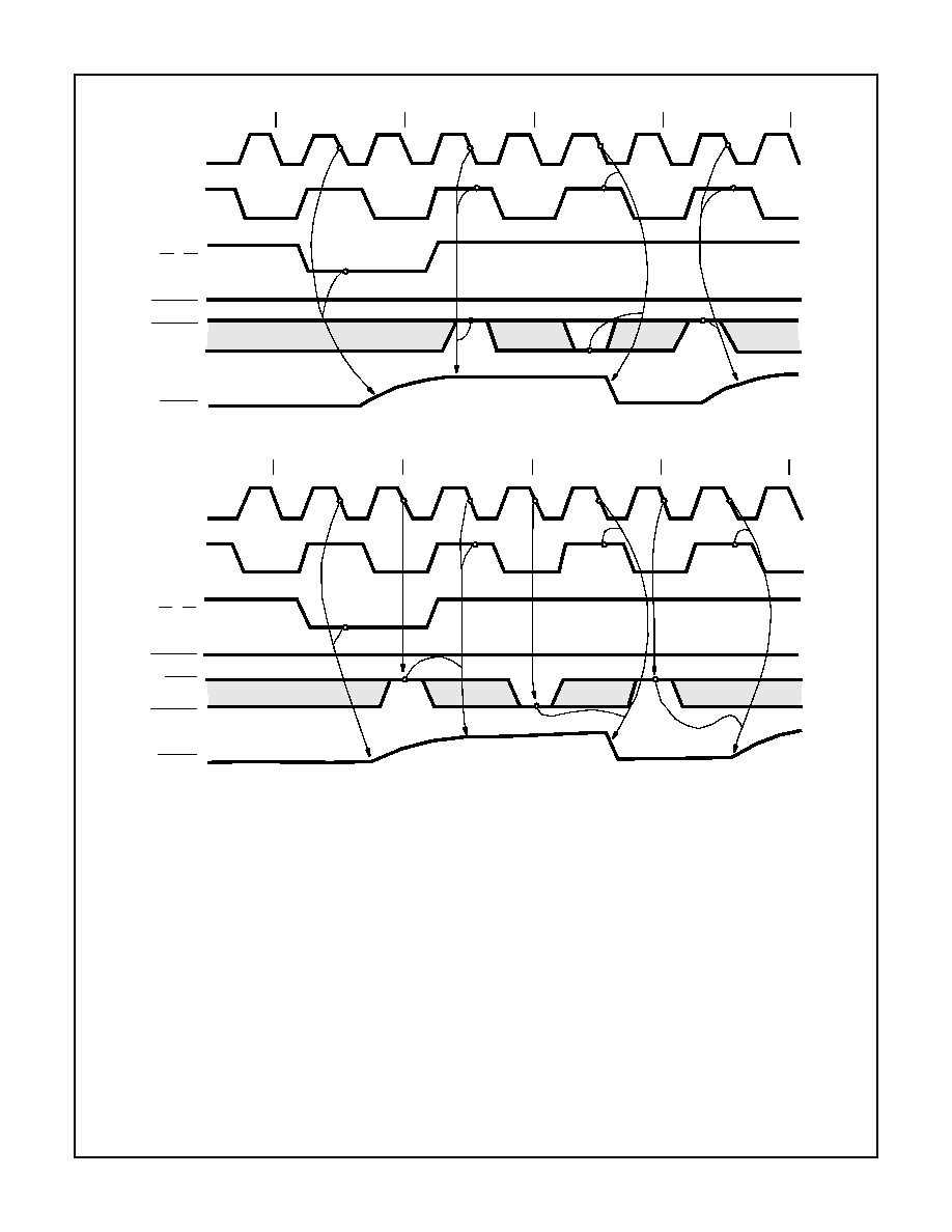
Figure 5 illustrates the operation of SRDY and SRDYEN.
These inputs are sampled on the falling edge of CLK when
S1 and S0 are inactive and PCLK is HIGH. READY is forced
active when both SRDY and SRDYEN are sampled as LOW.
Figure 6 shows the operation of ARDY and ARDYEN These
inputs are sampled by an internal synchronizer at each fall-
ing edge of CLK. The output of the synchronizer is then sam-
pled when PCLK is HIGH. If the synchronizer resolved both
the ARDY and ARDYEN as active, the SRDY and SRDYEN
inputs are ignored. Either ARDY or ARDYEN must be HIGH
at the end of T
S
, therefore, at least one wait state is required
when using the ARDY and ARDYEN inputs as a basis for
generating READY.
READY remains active until either S1 or S0 are sampled
LOW, or the ready inputs are sampled as inactive.
1N914
10k
V
CC
FIGURE 3. TYPICAL RC RES TIMING CIRCUIT
10
µ
F
11
82C284
RES
+
47
C1
7
8
X1
X2
F/C
82C284
CLK
READY
V
CC
CLK
80C286
CPU OR
SUPPORT
COMPONENT
READY
6
10
4
18
V
CC
DECOUPLING
CAPACITOR
FIGURE 4. RECOMMENDED CRYSTAL AND READY
CONDITIONS
V
CC
82C284

6
T
S
T
C
T
C
T
1
CLK
PCLK
S1 * S0
V
IH
ARDYEN
SRDYEN
+
SRDY
READY
FIGURE 5. SYNCHRONOUS READY OPERATION
FIGURE 6. ASYNCHRONOUS READY OPERATION
CLK
PCLK
S1 * S0
V
IH
SRDYEN
ARDY
+
ARDYEN
READY
T
S
T
C
T
C
T
1
82C284

7
Absolute Maximum Ratings
Thermal Information
Supply Voltage . . . . . . . . . . . . . . . . . . . . . . . . . . . . . . . . . . . . . +8.0V
Input, Output or I/O Voltage Applied. . . . . GND -0.5V to V
CC
+0.5V
Storage Temperature Range . . . . . . . . . . . . . . . . . -65
o
C to +150
o
C
Thermal Resistance
JA
(
o
C/W)
JC
(
o
C/W)
CERDIP Package . . . . . . . . . . . . . . . .
80
20
Gate Count . . . . . . . . . . . . . . . . . . . . . . . . . . . . . . . . . . . . 200 Gates
Junction Temperature . . . . . . . . . . . . . . . . . . . . . . . . . . . . . . +175
o
C
Lead Temperature (Soldering, 10s) . . . . . . . . . . . . . . . . . . . +300
o
C
ESD Classification. . . . . . . . . . . . . . . . . . . . . . . . . . . . . . . . . Class 2
Operating Conditions
Operating Temperature Range
C82C284. . . . . . . . . . . . . . . . . . . . . . . . . . . . . . . . . .0
o
C to +70
o
C
I82C284 . . . . . . . . . . . . . . . . . . . . . . . . . . . . . . . . -40
o
C to +85
o
C
Operating Supply Voltage . . . . . . . . . . . . . . . . . . . . . +4.5V to +5.5V
EFI Rise Time (from 0.8V to 3.2V) . . . . . . . . . . . . . . . . . . 8ns (Max)
EFI Fall Time (from 3.2 to 0.8V) . . . . . . . . . . . . . . . . . . . . 8ns (Max)
CAUTION: Stresses above those listed in "Absolute Maximum Ratings" may cause permanent damage to the device. This is a stress only rating and operation
of the device at these or any other conditions above those indicated in the operational sections of this specification is not implied.
DC Electrical Specifications
T
A
= 0
o
C to +70
o
C (CD82C284); V
CC
= 5V
±
10%
T
A
= -40
o
C to +85
o
C (ID82C284)
SYMBOL
PARAMETER
MIN
MAX
UNITS
TEST CONDITIONS
V
IL
Input LOW Voltage
-
0.8
V
V
CC
= 4.5V
V
IH
Input HIGH Voltage
2.2
-
V
V
CC
= 5.5V
V
IHC
EFI, F/C Input HIGH Voltage
3.2
-
V
V
CC
= 5.5V
V
IHR
RES HIGH Voltage
V
CC
-0.8
-
V
V
CC
= 5.5V
V
HYS
RES Input Hysteresis
0.5
-
V
V
CC
= 5.5V
V
OL
RESET, PCLK Output LOW Voltage
-
0.4
V
I
OL
= 5mA, V
CC
= 4.5V, Note 2
V
OH
RESET, PCLK Output HIGH Voltage
V
CC
-0.4
-
V
I
OH
= -1mA, V
CC
= 4.5V, Note 2
V
OLR
READY Output LOW Voltage
-
0.4
V
I
OL
= 10mA, V
CC
= 4.5V, Note 2
V
OLC
CLK Output LOW Voltage
-
0.4
V
I
OL
= 5mA, V
CC
= 4.5V, Note 2
V
OHC
CLK Output HIGH Voltage
V
CC
-0.4
-
V
I
OH
= -5mA, V
CC
= 4.5V, Note 2
I
IL
Input Leakage Current
-10
10
µ
A
V
IN
= V
CC
or GND, V
CC
= 5.5V
I
CCOP
Active Power Supply Current
-
60
mA
82C284-12 (Note 1)
-
48
mA
82C284-10 (Note 1)
NOTES:
1. I
CCOP
measured at 10MHz for 82C284-10 and at 12.5MHz for the 82C284-12. V
IN
= GND or V
CC
, V
CC
= 5.5V outputs unloaded.
2. Interchanging of force and sense conditions is permitted.
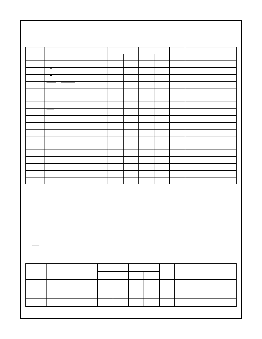
AC Electrical Specifications
T
A
= 0
o
C to +70
o
C (CD82C284); V
CC
= 5V
±
10%
T
A
= -40
o
C to +85
o
C (lD82C284)
AC Timings are Referenced to 0.8V and 2.0V Points of the Signals as Illustrated in Waveforms,
Unless Otherwise Noted.
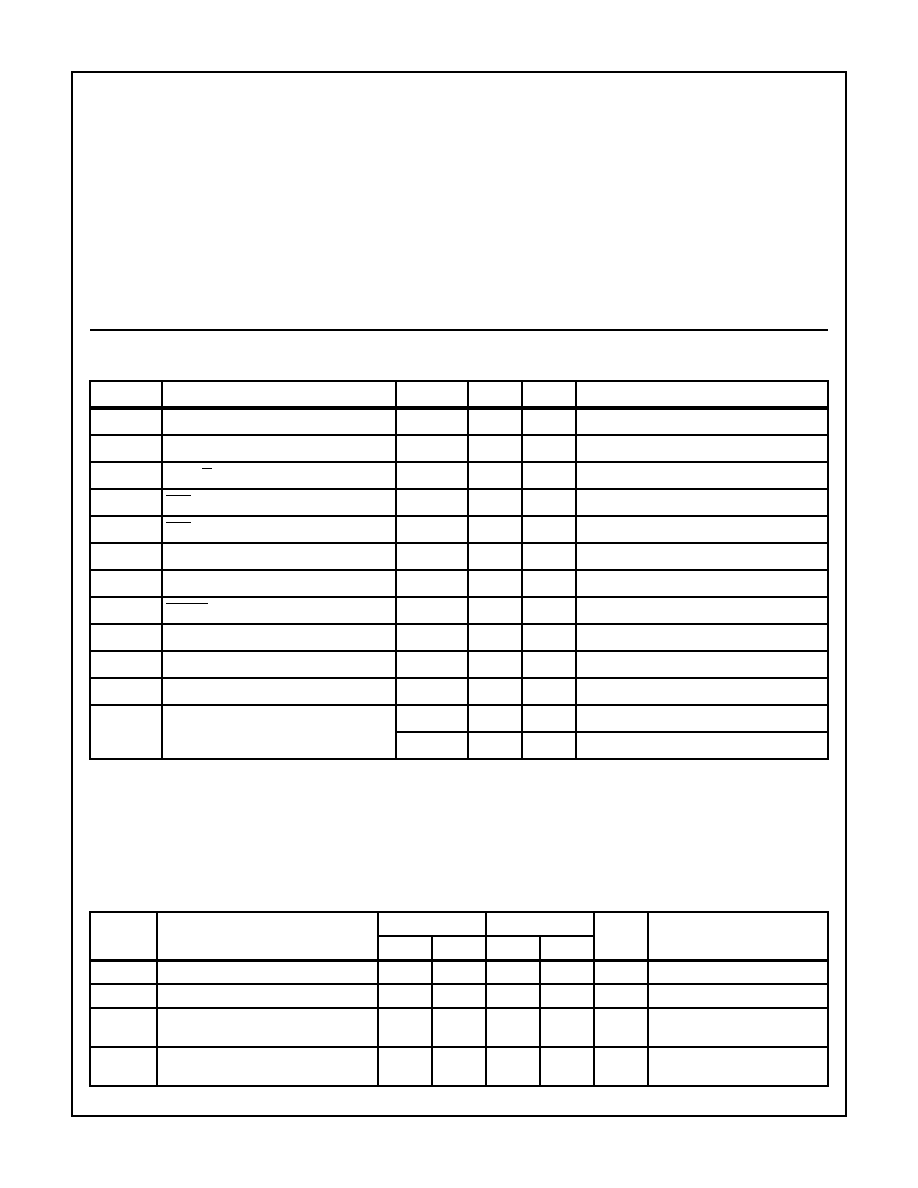
SYMBOL
PARAMETER
10MHz
12.5MHz
UNIT
TEST CONDITIONS
MIN
MAX
MIN
MAX
t1
EFl LOW Time
20
-
16
-
ns
At V
CC
/2 (Note 8)
t2
EFI HIGH Time
20
-
20
-
ns
At V
CC
/2 (Note 8)
5A
Status Setup Time for Status Going
Active
20
-
18
-
ns
5B
Status Setup Time for Status Going
Inactive
20
-
16
-
ns
82C284

8
t6
Status Hold Time
1
-
1
-
ns
t7
F/C Setup Time
15
-
15
-
t8
F/C Hold Time
15
-
15
-
t9
SRDY or SRDYEN Setup Time
15
-
15
-
ns
t10
SRDY or SRDYEN Hold Time
2
-
2
-
ns
t11
ARDY or ARDYEN Setup Time
5
-
5
-
ns
(Note 3)
t12
ARDY or ARDYEN Hold Time
30
-
25
-
ns
(Note 3)
t13
RES Setup Time
20
-
18
-
ns
(Notes 3, 7)
t14
RES Hold Time
10
-
8
-
ns
(Notes 3, 7)
t16
CLK Period
50
-
40
-
t17
CLK LOW Time
12
-
11
-
ns
(Notes 2, 6)
t18
CLK HIGH Time
16
-
13
-
ns
(Notes 2, 6)
t21
READY Inactive Delay
5
-
5
-
ns
At 0.8V (Note 4), Test Condition 2
t22
READY Active Delay
-
24
-
18
ns
At 0.8V (Note 4)
t23
PCLK Delay
-
20
-
16
ns
C
L
= 75pF, Test Condition 1
t24
RESET Delay
-
27
-
26
ns
C
L
= 75pF, Test Condition 3
t25
PCLK LOW Time
t16 -10
-
t16 -10
-
na
C
L
= 75pF (Note 5)
t26
PCLK HIGH Time
t16 -10
-
t16 -10
-
ns
C
L
= 75pF (Note 5)
NOTES:
1. V
CC
= 4.5V and 5.5V unless otherwise specified. CLK loading: C
L
= 100pF.
2. With the internal crystal oscillator using recommended crystal and capacitive loading; or with the EFI input meeting specifications t
1
and
t
2
. The recommended crystal loading for CLK frequencies of 8MHz to 20MHz are 25pF from pin X1 to ground, and 15pF from pin X2 to
ground; for CLK frequencies from 20MHz to 25MHz the recommended loading is 15pF from pin X1 to GND. These recommended values
are +5pF and include all stray capacitance. Decouple V
CC
and GND as close to the 82C284 as possible.
3. This is an asynchronous input. This specification is given for testing purposes only, to assure recognition at a specific CLK edge.
4. The pull-up resistor value for the READY pin is 620
with the rated 150pF load.
5. t
16
refers to any allowable CLK period.
6. When using a crystal with the recommended capacitive loading, CLK output HIGH and LOW times are guaranteed to meet 80C286 re-
quirements.
7. Measured from 1.0V on the CLK to 0.8V on the RES waveform for RES waveform for RES active and to 4.2V on the RES waveform for
RES inactive.
8. Input test waveform characteristics: V
IL
= 0V, V
lH
= 4.5V.
AC Electrical Specifications
T
A
= 0
o
C to +70
o
C (CD82C284); V
CC
= 5V
±
10% (Continued)
T
A
= -40
o
C to +85
o
C (lD82C284)
AC Timings are Referenced to 0.8V and 2.0V Points of the Signals as Illustrated in Waveforms,
Unless Otherwise Noted.
SYMBOL
PARAMETER
10MHz
12.5MHz
UNIT
TEST CONDITIONS
MIN
MAX
MIN
MAX
UNTESTED SPECIFICATIONS
SYMBOL
PARAMETER
10MHz
12.5MHz
UNITS
CONDlTIONS (NOTE 1)
MIN
MAX
MIN
MAX
C
IN
Input Capacitance
-
10
-
10
pF
FREQ = 1MHz, All measurements are
referenced to device GND, T
A
= +25
o
C
t15A
EFI HIGH to CLK LOW Delay
-
30
-
25
ns
(Note 2)
t15B
EFI LOW to CLK HIGH Delay
-
35
-
30
ns
(Note 3)
82C284

9
AC Specifications
AC Test Condition
t19
CLK Rise Time
-
8
-
8
ns
1.0V to 3.6V, C
L
= 100pF
t20
CLK Fall Time
-
8
-
8
ns
3.6V to 1.0V, C
L
= 100pF
t27
X1 HIGH to CLK
-
35
-
30
ns
(Note 4)
NOTES:
1. The parameters listed in this table are controlled via design or, process parameters and are not directly tested. These parameters are
characterized upon initial design and after major process and/or design changes.
2. Measured from 3.2V on the EFI waveform to 1.0V on the CLK.
3. Measured from 0.8V on the EFI waveform to 3.6V on the CLK.
4. Measured from 3.6V on the X1 input to 3.6V on the CLK.
UNTESTED SPECIFICATIONS (Continued)
SYMBOL
PARAMETER
10MHz
12.5MHz
UNITS
CONDlTIONS (NOTE 1)
MIN
MAX
MIN
MAX
3.2V
3.8V
0.4V
0.8V
3.6V
1.0V
3.6V
1.0V 0.4V
3.8V
0.4V
V
CC
- 0.4V
0.4V
2.4
0.4V
V
CC
- 0.4V
t
SETUP
3.2V
0.8V
3.2V
0.8V
0.8V
2.0V
0.8V
2.0V
0.8V
t
DELAY
(MIN)
t
DELAY
(MAX)
EFI INPUT
CLK
F/C
RES
OTHER
DEVICE
t
HOLD
0.8V
2.0V
0.8V
OUTPUT
DEVICE
INPUT
INPUT
INPUT
OUTPUT
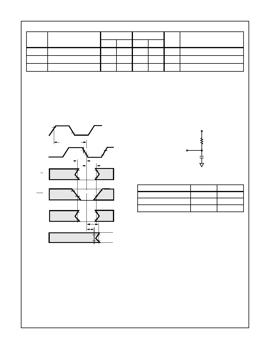
FIGURE 7. A.C. DRIVE, SETUP, HOLD AND DELAY TIME
MEASUREMENT POINTS
t
DELAY
(MAX)
VCC - 0.8V
TEST CONDITION
R
L
C
L
1
750
75pF
2
620
150pF
3
75pF
V
CC
R
L
C
L
DEVICE
OUTPUT
FIGURE 8.
82C284

10
Waveforms
NOTE:
1. The EFI input LOW and HIGH times as shown are required to guarantee the CLK LOW and HIGH times shown.
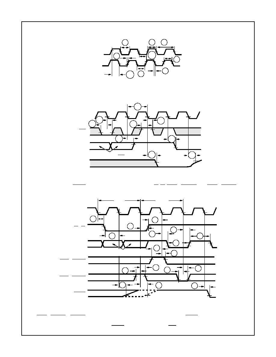
FIGURE 9. CLK AS A FUNCTION OF EFI
NOTE:
1. This is an asynchronous input. The setup and hold times shown are required to guarantee the response shown.
FIGURE 10. RESET AND READY TIMING AS A FUNCTION OF RES WITH S1, S0, ARDY + ARDYEN, AND SRDY + SRDYEN HIGH
NOTES:
1. This is an asynchronous input. The setup and hold times shown are required to guarantee the response shown.
2. If SRDY + SRDYEN or ARDYEN are active before and/or during the first bus cycle after RESET, READY may not be deasserted until the
falling edge of
2 of T
S
.
FIGURE 11. READY AND PCLK TIMING WITH RES HIGH
EFI
CLK
t
15B
t
19
t
1
t
2
t
17
t
20
t
18
t
16
t
15A
t
16
t
13
t
14
t
14
t
13
t
24
t
22
t
24
t
21
SEE
NOTE
DEPENDS ON STATE
OF PREVIOUS RES
CLK
RES
RESET
READY
t
6
t
5A
t
6
t
5B
t
23
t
23
t
21
t
11
t
21
t
12
t
9
t
11
t
10
t
25
t
26
t
12
t
22
T
S
T
C
1
2
1
2
CLK
S1
∑
S0
PCLK
SRDY + SRDYEN
ARDY + ARDYEN
READY
NOTE 2
NOTE 1
UNDEFINED IF THIS IS
FIRST BUS CYCLE
82C284

11
All Intersil U.S. products are manufactured, assembled and tested utilizing ISO9000 quality systems.
Intersil Corporation's quality certifications can be viewed at www.intersil.com/design/quality
Intersil products are sold by description only. Intersil Corporation reserves the right to make changes in circuit design, software and/or specifications at any time without
notice. Accordingly, the reader is cautioned to verify that data sheets are current before placing orders. Information furnished by Intersil is believed to be accurate and
reliable. However, no responsibility is assumed by Intersil or its subsidiaries for its use; nor for any infringements of patents or other rights of third parties which may result
from its use. No license is granted by implication or otherwise under any patent or patent rights of Intersil or its subsidiaries.
For information regarding Intersil Corporation and its products, see www.intersil.com
Sales Office Headquarters
NORTH AMERICA
Intersil Corporation
7585 Irvine Center Drive
Suite 100
Irvine, CA 92618
TEL: (949) 341-7000
FAX: (949) 341-7123
Intersil Corporation
2401 Palm Bay Rd.
Palm Bay, FL 32905
TEL: (321) 724-7000
FAX: (321) 724-7946
EUROPE
Intersil Europe Sarl
Ave. William Graisse, 3
1006 Lausanne
Switzerland
TEL: +41 21 6140560
FAX: +41 21 6140579
ASIA
Intersil Corporation
Unit 1804 18/F Guangdong Water Building
83 Austin Road
TST, Kowloon Hong Kong
TEL: +852 2723 6339
FAX: +852 2730 1433
NOTE:
1. This is an asynchronous input. The setup and hold times are required to guarantee the response shown.
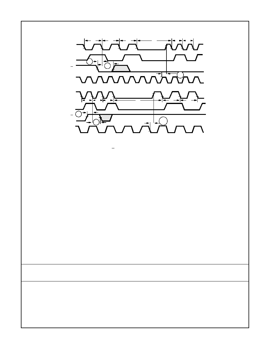
FIGURE 12. CLK AS A FUNCTION OF F/C, PCLK, X1, AND EFI DURING DYNAMIC FREQUENCY SWITCHING
Waveforms
(Continued)
CLK
1
2
2
1
2
t
7
t
8
2
2
2
1
1
1
t
7
t
8
t
15B
t
27
PCLK
F/C
CLK
PCLK
F/C
X1
EFI
1
82C284


