 | –≠–ª–µ–∫—Ç—Ä–æ–Ω–Ω—ã–π –∫–æ–º–ø–æ–Ω–µ–Ω—Ç: 84069012A | –°–∫–∞—á–∞—Ç—å:  PDF PDF  ZIP ZIP |

4-333
March 1997
82C88
CMOS Bus Controller
Features
∑ Compatible with Bipolar 8288
∑ Performance Compatible with:
- 80C86/80C88 . . . . . . . . . . . . . . . . . . . . . . . . . .(5/8MHz)
- 80186/80188 . . . . . . . . . . . . . . . . . . . . . . . . . .(6/8MHz)
- 8086/8088 . . . . . . . . . . . . . . . . . . . . . . . . . . . .(5/8MHz)
- 8089
∑ Provides Advanced Commands for Multi-Master
Busses
∑ Three-State Command Outputs
∑ Bipolar Drive Capability
∑ Scaled SAJI IV CMOS Process
∑ Single 5V Power Supply
∑ Low Power Operation
- ICCSB . . . . . . . . . . . . . . . . . . . . . . . . . . . . 10
µ
A (Max)
- ICCOP . . . . . . . . . . . . . . . . . . . . . . . . .1mA/MHz (Max)
∑ Operating Temperature Ranges
- C82C88 . . . . . . . . . . . . . . . . . . . . . . . . . .0
o
C to +70
o
C
- I82C88 . . . . . . . . . . . . . . . . . . . . . . . . . -40
o
C to +85
o
C
- M82C88 . . . . . . . . . . . . . . . . . . . . . . . -55
o
C to +125
o
C
Description
The Intersil 82C88 is a high performance CMOS Bus Con-
troller manufactured using a self-aligned silicon gate CMOS
process (Scaled SAJI IV). The 82C88 provides the control
and command timing signals for 80C86, 80C88, 8086, 8088,
8089, 80186, and 80188 based systems. The high output
drive capability of the 82C88 eliminates the need for addi-
tional bus drivers.
Static CMOS circuit design insures low operating power. The
Intersil advanced SAJI process results in performance equal
to or greater than existing equivalent products at a significant
power savings.
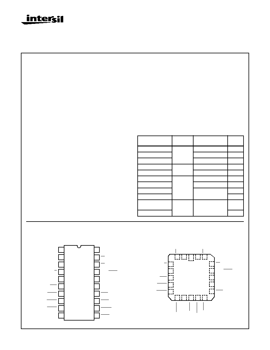
Pinouts
20 LEAD PDIP, CERDIP
TOP VIEW
20 LEAD PLCC, CLCC
TOP VIEW
Ordering Information
PART NUMBER
PACKAGE
TEMPERATURE
RANGE
PKG.
NO.
CP82C88
20 Ld PDIP
0
o
C to +70
o
C
E20.3
CP82C88-10
0
o
C to +70
o
C
E20.3
IP82C88
-40
o
C to +85
o
C
E20.3
CS82C88
20 Ld
PLCC
0
o
C to +70
o
C
N20.35
IS82C88
-40
o
C to +85
o
C
N20.35
CD82C88
20 Ld
CERDIP
0
o
C to +70
o
C
F20.3
ID82C88
-40
o
C to +85
o
C
F20.3
MD82C88/B
-55
o
C to +125
o
C
F20.3
8406901RA
SMD#
F20.3
MR82C88/B
20 Pad
CLCC
-55
o
C to +125
o
C
J20.A
84069012A
SMD#
J20.A
11
12
13
14
15
16
17
18
19
20
10
9
8
7
6
5
4
3
2
1
IOB
CLK
ALE
GND
DT/ R
AEN
MRDC
AMWC
MWTC
S1
V
CC
MCE/PDEN
DEN
CEN
IORC
AIOWC
IOWC
INTA
S0
S2
4
5
6
7
8
9
10
11
12
13
3
2
1
20
19
15
14
18
17
16
ALE
DT/ R
AEN
MRDC
AMWC
GND
IORC
AIO
WC
IO
WC
MWTC
V
CC
IOB
CLK
S1
S0
DEN
CEN
MCE/PDEN
INTA
S2
File Number
2979.1
CAUTION: These devices are sensitive to electrostatic discharge; follow proper IC Handling Procedures.
http://www.intersil.com or 407-727-9207
|
Copyright
©
Intersil Corporation 1999

4-334
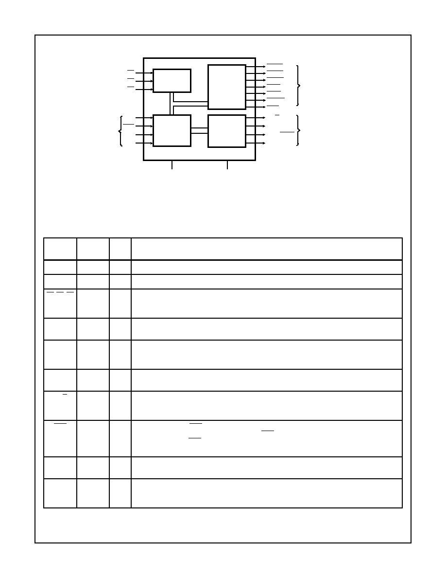
Functional Diagram
Pin Description
PIN
SYMBOL
NUMBER
TYPE
DESCRIPTION
V
CC
20
V
CC
: The +5V power supply pin. A 0.1
µ
F capacitor between pins 10 and 20 is recommended for decoupling.
GND
10
GROUND.
S0, S1, S2
19, 3, 18
I
STATUS INPUT PINS: These pins are the input pins from the 80C86, 80C88,8086/88, 8089 processors.
The 82C88 decodes these inputs to generate command and control signals at the appropriate time.
When Status pins are not in use (passive), command outputs are held HIGH (See Table1).
CLK
2
I
CLOCK: This is a CMOS compatible input which receives a clock signal from the 82C84A or 82C85 clock
generator and serves to establish when command/control signals are generated.
ALE
5
O
ADDRESS LATCH ENABLE: This signal serves to strobe an address into the address latches. This sig-
nal is active HIGH and latching occurs on the falling (HIGH to LOW) transition. ALE is intended for use
with transparent D type latches, such as the 82C82 and 82C83H.
DEN
16
O
DATA ENABLE: This signal serves to enable data transceivers onto either the local or system data bus.
This signal is active HIGH.
DT/R
4
O
DATA TRANSMIT/RECEIVE: This signal establishes the direction of data flow through the transceivers.
A HIGH on this line indicates Transmit (write to I/O or memory) and a LOW indicates Receive (read from
I/O or memory).
AEN
6
I
ADDRESS ENABLE: AEN enables command outputs of the 82C88 Bus Controller a minimum of 110ns
(250ns maximum) after it becomes active (LOW). AEN going inactive immediately three-states the com-
mand output drivers. AEN does not affect the I/O command lines if the 82C88 is in the I/O Bus mode
(IOB tied HIGH).
CEN
15
I
COMMAND ENABLE: When this signal is LOW all 82C88 command outputs and the DEN and PDEN con-
trol outputs are forced to their Inactive state. When this signal is HIGH, these same outputs are enabled.
IOB
1
I
INPUT/OUTPUT BUS MODE: When the IOB pin is strapped HIGH, the 82C88 functions in the I/O Bus
mode. When it is strapped LOW, the 82C88 functions in the System Bus mode (See I/O Bus and System
Bus sections).
V
CC
GND
COMMAND
SIGNALS
MULTIBUS
TM
CONTROL
INPUT
IOB
CEN
CLK
AEN
CONTROL
SIGNAL
GENERATOR
DEN
ALE
DT/R
MCE/PDEN
COMMAND
SIGNAL
GENERATOR
AIOWC
IOWC
AMWC
MWTC
MRDC
IORC
S2
S1
S0
INTA
ADDRESS LATCH,
DATA TRANSCEIVER,
AND INTERRUPT
CONTROL SIGNALS
CONTROL
LOGIC
STATUS
DECODER
82C88
IntelTM is a Registered Trademark of Intel Corporation

4-335
Functional Description
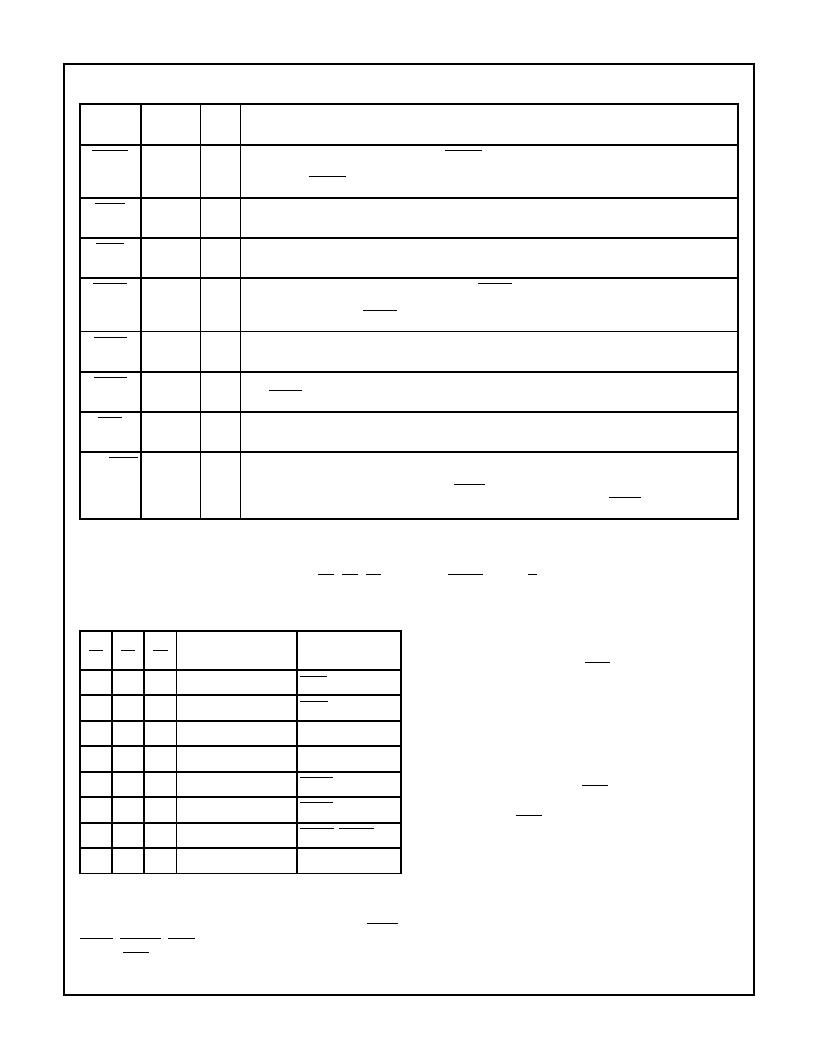
The command logic decodes the three 80C86, 8086, 80C88,
8088, 80186, 80188 or 8089 status lines (S0, S1, S2) to
determine what command is to be issued (see Table 1).
I/O Bus Mode
The 82C88 is in the I/O Bus mode if the IOB pin is strapped
HIGH. In the I/O Bus mode, all I/O command lines IORC,
IOWC, AIOWC, INTA) are always enabled (i.e., not depen-
dent on AEN). When an I/O command is initiated by the pro-
cessor, the 82C88 immediately activates the command lines
using PDEN and DT/R to control the I/O bus transceiver. The
I/O command lines should not be used to control the system
bus in this configuration because no arbitration is present.
This mode allows one 82C88 Bus Controller to handle two
external busses. No waiting is involved when the CPU wants
to gain access to the I/O bus. Normal memory access
requires a "Bus Ready" signal (AEN LOW) before it will pro-
ceed. It is advantageous to use the IOB mode if I/O or
peripherals dedicated to one processor exist in a multi-pro-
cessor system.
System Bus Mode
The 82C88 is in the System Bus mode if the IOB pin is
strapped LOW. In this mode, no command is issued until a
specified time period after the AEN line is activated (LOW).
This mode assumes bus arbitration logic will inform the bus
controller (on the AEN line) when the bus is free for use.
Both memory and I/O commands wait for bus arbitration.
This mode is used when only one bus exists. Here, both I/O
and memory are shared by more than one processor.
Command Outputs
The advanced write commands are made available to initiate
write procedures early in the machine cycle. This signal can
be used to prevent the processor from entering an unneces-
sary wait state.
AIOWC
12
O
ADVANCED I/O WRITE COMMAND: The AIOWC issues an I/O Write Command earlier in the machine
cycle to give I/O devices an early indication of a write instruction. Its timing is the same as a read com-
mand signal. AIOWC is active LOW.
IOWC
11
O
I/O WRITE COMMAND: This command line instructs an I/O device to read the data on the data bus. The
signal is active LOW.
IORC
13
O
I/O READ COMMAND: This command line instructs an I/O device to drive its data onto the data bus. This
signal is active LOW.
AMWC
8
O
ADVANCED MEMORY WRITE COMMAND: The AMWC issues a memory write command earlier in the
machine cycle to give memory devices an early indication of a write instruction. Its timing is the same as
a read command signal. AMWC is active LOW.
MWTC
9
O
MEMORY WRITE COMMAND: This command line instructs the memory to record the data present on
the data bus. This signal is active LOW.
MRDC
7
O
MEMORY READ COMMAND: This command line instructs the memory to drive its data onto the data
bus. MRDC is active LOW.
INTA
14
O
INTERRUPT ACKNOWLEDGE: This command line tells an interrupting device that its interrupt has been
acknowledged and that it should drive vectoring information onto the data bus. This signal is active LOW.
MCE/PDEN
17
O
This is a dual function pin. MCE (IOB IS TIED LOW) Master Cascade Enable occurs during an interrupt
sequence and serves to read a Cascade Address from a master 82C59A Priority Interrupt Controller onto
the data bus. The MCE signal is active HIGH. PDEN (IOB IS TIED HIGH): Peripheral Data Enable enables
the data bus transceiver for the I/O bus that DEN performs for the system bus. PDEN is active LOW.
Pin Description
(Continued)
PIN
SYMBOL
NUMBER
TYPE
DESCRIPTION
TABLE 1. COMMAND DECODE DEFINITION
S2
S1
S0
PROCESSOR STATE
82C88
COMMAND
0
0
0
Interrupt Acknowledge
INTA
0
0
1
Read I/O Port
IORC
0
1
0
Write I/O Port
IOWC, AIOWC
0
1
1
Halt
None
1
0
0
Code Access
MRDC
1
0
1
Read Memory
MRDC
1
1
0
Write Memory
MWTC, AMWC
1
1
1
Passive
None
82C88

4-336
INTA (Interrupt Acknowledge) acts as an I/O read during an
interrupt cycle. Its purpose is to inform an interrupting device
that its interrupt is being acknowledged and that it should
place vectoring information onto the data bus.
The command outputs are:
MRDC - Memory Read Command
MWTC - Memory Write Command
IORC - I/O Read Command
IOWC - I/O Write Command
AMWC - Advanced Memory Write Command
AIOWC - Advanced I/O Write Command
INTA - Interrupt Acknowledge
Control Outputs
The control outputs of the 82C88 are Data Enable (DEN),
Data Transmit/Receive (DT/R) and Master Cascade Enable/
Peripheral Data Enable (MCE/PDEN). The DEN signal
determines when the external bus should be enabled onto
the local bus and the DT/R determines the direction of data
transfer. These two signals usually go to the chip select and
direction pins of a transceiver.
The MCE/PDEN pin changes function with the two modes of
the 82C88. When the 82C88 is in the IOB mode (IOB HIGH),
the PDEN signal serves as a dedicated data enable signal
for the I/O or Peripheral System bus.
Interrupt Acknowledge and MCE
The MCE signal is used during an interrupt acknowledge
cycle if the 82C88 is in the System Bus mode (IOB LOW).
During any interrupt sequence, there are two interrupt
acknowledge cycles that occur back to back. During the first
interrupt cycle no data or address transfers take place. Logic
should be provided to mask off MCE during this cycle. Just
before the second cycle begins the MCE signal gates a mas-
ter Priority Interrupt Controller's (PIC) cascade address onto
the processor's local bus where ALE (Address Latch Enable)
strobes it into the address latches. On the leading edge of
the second interrupt cycle, the addressed slave PIC gates an
interrupt vector onto the system data bus where it is read by
the processor.
If the system contains only one PIC, the MCE signal is not
used. In this case, the second Interrupt Acknowledge signal
gates the interrupt vector onto the processor bus.
Address Latch Enable and Halt
Address Latch Enable (ALE) occurs during each machine
cycle and serves to strobe the current address into the
82C82/82C83H address latches. ALE also serves to strobe
the status (S0, S1, S2) into a latch for halt state decoding.
Command Enable
The Command Enable (CEN) input acts as a command
qualifier for the 82C88. If the CEN pin is high, the 82C88
functions normally. If the CEN pin is pulled LOW, all com-
mand lines are held in their inactive state (not three-state).
This feature can be used to implement memory partitioning
and to eliminate address conflicts between system bus
devices and resident bus devices.
82C88

4-337
Absolute Maximum Ratings
Thermal Information
Supply Voltage . . . . . . . . . . . . . . . . . . . . . . . . . . . . . . . . . . . . . +8.0V
Input, Output or I/O Voltage . . . . . . . . . . . GND -0.5V to V
CC
+0.5V
ESD Classification . . . . . . . . . . . . . . . . . . . . . . . . . . . . . . . . Class 1
Operating Conditions
Operating Voltage Range . . . . . . . . . . . . . . . . . . . . . +4.5V to +5.5V
Operating Temperature Range
C82C88. . . . . . . . . . . . . . . . . . . . . . . . . . . . . . . . . . 0
o
C to +70
o
C
I82C88 . . . . . . . . . . . . . . . . . . . . . . . . . . . . . . . . . -40
o
C to +85
o
C
M82C88 . . . . . . . . . . . . . . . . . . . . . . . . . . . . . . . -55
o
C to +125
o
C
Thermal Resistance (Typical)
JA
(
o
C/W)
JC
(
o
C/W)
CERDIP Package . . . . . . . . . . . . . . . .
75
18
CLCC Package . . . . . . . . . . . . . . . . . .
85
22
PDIP Package . . . . . . . . . . . . . . . . . . .
75
N/A
PLCC Package . . . . . . . . . . . . . . . . . .
75
N/A
Storage Temperature Range . . . . . . . . . . . . . . . . . .-65
o
C to +150
o
C
Maximum Junction Temperature
Ceramic Package . . . . . . . . . . . . . . . . . . . . . . . . . . . . . . . +175
o
C
Plastic Package . . . . . . . . . . . . . . . . . . . . . . . . . . . . . . . . . +150
o
C
Maximum Lead Temperature (Soldering 10s) . . . . . . . . . . . . +300
o
C
(PLCC - Lead Tips Only)
Die Characteristics
Gate Count . . . . . . . . . . . . . . . . . . . . . . . . . . . . . . . . . . . . 100 Gates
CAUTION: Stresses above those listed in "Absolute Maximum Ratings" may cause permanent damage to the device. This is a stress only rating and operation
of the device at these or any other conditions above those indicated in the operational sections of this specification is not implied.
DC Electrical Specifications
V
CC
= 5.0V
±
10%;
T
A
= 0
o
C to +70
o
C (C82C88);
T
A
= -40
o
C to +85
o
C (I82C88);
T
A
= -55
o
C to +125
o
C (M82C88)
SYMBOL
PARAMETER
MIN
MAX
UNITS
TEST CONDITIONS
V
IH
Logical One Input Voltage
2.0
2.2
-
-
V
V
C82C88, I82C88
M82C88
V
IL
Logical Zero Input Voltage
-
0.8
V
VIHC
CLK Logical One Input Voltage
V
CC
-0.8
-
V
VILC
CLK Logical Zero Input Voltage
-
0.8
V
V
OH
Output High Voltage
Command Outputs
3.0
V
CC
-0.4
-
V
V
I
OH
= -8.0mA
I
OH
= -2.5mA
Output High Voltage
Control Outputs
3.0
V
CC
-0.4
-
V
V
I
OH
= -4.0mA
I
OH
= -2.5mA
V
OL
Output Low Voltage
Command Outputs
-
0.5
V
I
OL
= +12.0mA
Output Low Voltage
Control Outputs
-
0.4
V
I
OL
= +8.0mA
I
I
Input Leakage Current
-1.0
1.0
µ
A
V
IN
= GND or V
CC
, except S0, S1, S2,
DIP Pins 1-2, 6, 15
IBHH
Input Leakage Current-Status Bus
-50
-300
µ
A
V
IN
= 2.0V, S0, S1, S2 (See Note 1)
IO
Output Leakage Current
-10.0
10.0
µ
A
V
O
= GND or V
CC
, IOB = GND, AEN = V
CC
,
DIP Pins 7-9, 11-14
ICCSB
Standby Power Supply
-
10
µ
A
V
CC
= 5.5V, V
IN
= V
CC
or GND, Outputs Open
ICCOP
Operating Power Supply Current
-
1
mA/MHz
V
CC
= 5.5V, Outputs Open (See Note 2)
NOTES:
1. IBHH should be measured after raising the V
IN
on S0, S1, S2 to V
CC
and then lowering to valid input high level of 2.0V.
2. ICCOP = 1mA/MHz of CLK cycle time (TCLCL)
Capacitance
T
A
= +25
o
C
SYMBOL
PARAMETER
TYPICAL
UNITS
TEST CONDITIONS
CIN
Input Capacitance
10
pF
FREQ = 1MHz, all measurements are
referenced to device GND
COUT
Output Capacitance
17
pF
82C88
