 | –≠–ª–µ–∫—Ç—Ä–æ–Ω–Ω—ã–π –∫–æ–º–ø–æ–Ω–µ–Ω—Ç: 8413203YA | –°–∫–∞—á–∞—Ç—å:  PDF PDF  ZIP ZIP |
6-1
March 1997
HM-65262
16K x 1 Asynchronous
CMOS Static RAM
Features
∑ Fast Access Time. . . . . . . . . . . . . . . . . . . . 70/85ns Max
∑ Low Standby Current. . . . . . . . . . . . . . . . . . . .50
µ
A Max
∑ Low Operating Current . . . . . . . . . . . . . . . . . 50mA Max
∑ Data Retention at 2.0V . . . . . . . . . . . . . . . . . . .20
µ
A Max
∑ TTL Compatible Inputs and Outputs
∑ JEDEC Approved Pinout
∑ No Clocks or Strobes Required
∑ Temperature Range . . . . . . . . . . . . . . . +55
o
C to +125
o
C
∑ Equal Cycle and Access Time
∑ Single 5V Supply
∑ Gated Inputs-No Pull-Up or Pull-Down Resistors
Required
Description
The HM-65262 is a CMOS 16384 x 1-bit Static Random
Access Memory manufactured using the Intersil Advanced
SAJI V process. The device utilizes asynchronous circuit
design for fast cycle times and ease of use. The HM-65262
is available in both JEDEC standard 20 pin, 0.300 inch wide
CERDIP and 20 pad CLCC packages, providing high board-
level packing density. Gated inputs lower standby current,
and also eliminate the need for pull-up or pull-down resis-
tors.
The HM-65262, a full CMOS RAM, utilizes an array of six
transistor (6T) memory cells for the most stable and lowest
possible standby supply current over the full military temper-
ature range. In addition to this, the high stability of the 6T
RAM cell provides excellent protection against soft errors
due to noise and alpha particles. This stability also improves
the radiation tolerance of the RAM over that of four transistor
(4T) devices.
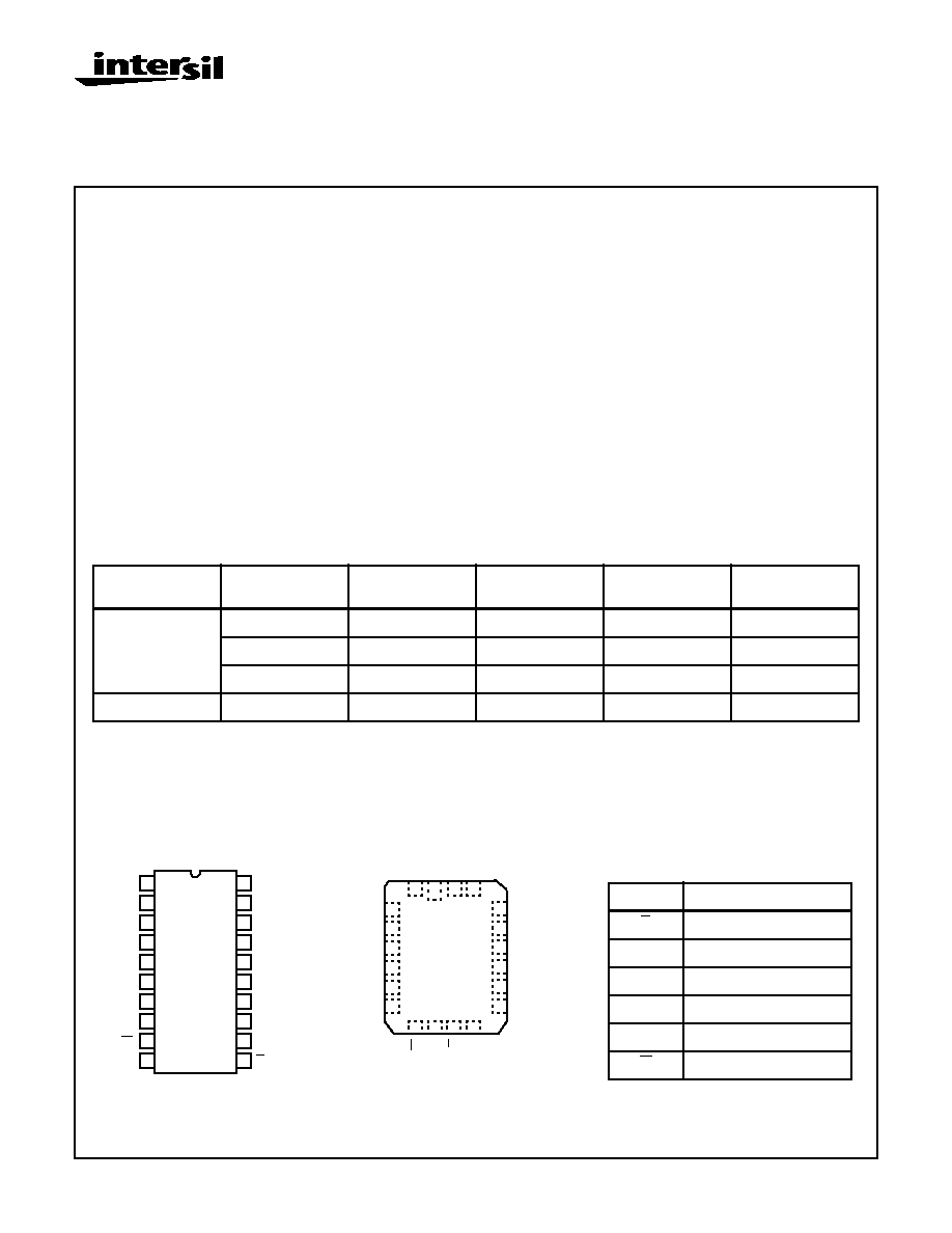
Pinouts
Ordering Information
PACKAGE
TEMP. RANGE
70ns/20
µ
A (NOTE 1) 85ns/20
µ
A (NOTE 1)
(NOTE 1)
85ns/400
µ
A
PKG. NO.
CERDIP
-40
o
C to +85
o
C
HM1-65262B-9
HM1-65262-9
-
F20.3
JAN #
-55
o
C to +125
o
C
29109BRA
29103BRA
-
F20.3
SMD#
-55
o
C to +125
o
C
8413203RA
8413201RA
-
F20.3
CLCC (SMD#)
-55
o
C to +125
o
C
8413203YA
8413201YA
-
J20.C
NOTE:
1. Access Time/Data Retention Supply Current.
HM-65262 (CERDIP)
TOP VIEW
HM-65262 (CLCC)
TOP VIEW
11
12
13
14
15
16
17
18
20
19
10
9
8
7
6
5
4
3
2
1
A0
A1
A2
A3
A4
A5
Q
A6
W
GND
V
CC
A12
A11
A10
A13
A9
A8
A7
D
E
3
4
5
6
7
9
10 11 12
2
20
1
19
8
15
14
18
17
16
13
A0
A1
A2
V
CC
A13
A3
A4
A5
A6
Q
A12
A11
A10
A9
A8
A7
W
GND
E
D
A0 - A13
Address Input
E
Chip Enable/Power Down
Q
Data Out
D
Data In
V
SS
/GND
Ground
V
CC
Power (+5)
W
Write Enable
File Number
3002.2
CAUTION: These devices are sensitive to electrostatic discharge; follow proper IC Handling Procedures.
http://www.intersil.com or 407-727-9207
|
Copyright
©
Intersil Corporation 1999
6-2
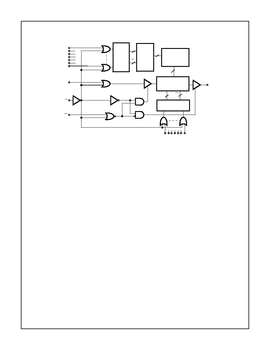
Functional Diagram
ROW
ADDRESS
BUFFER
128
7
7
A0
A1
A2
A3
A12
A13
128
128 X 128
MEMORY ARRAY
A
7
A
7
A
A
ROW
DECODER
(1 OF 128)
A4
COLUMN DECODER
(1 OF 128)
AND I / O CIRCUITRY
Q
W
E
D
A7
A6
A8 A9
A10
A11
A5
COLUMN
ADDRESS BUFFERS
HM-65262
6-3
Absolute Maximum Ratings
Thermal Information
Supply Voltage . . . . . . . . . . . . . . . . . . . . . . . . . . . . . . . . . . . . . . . . +7.0V
Input or Output Voltage Applied for all grades . . . . . -0.3V to V
CC
+0.3V
Typical Derating Factor . . . . . . . . . . . . . . . .5mA/MHz Increase in ICCOP
ESD Classification . . . . . . . . . . . . . . . . . . . . . . . . . . . . . . . . . . . . Class 1
Thermal Resistance (Typical)
JA
JC
CERDIP Package . . . . . . . . . . . . . . . . . .
66
o
C/W
13
o
C/W
CLCC Package. . . . . . . . . . . . . . . . . . . .
75
o
C/W
18
o
C/W
Maximum Storage Temperature Range . . . . . . . . . . . . . -65
o
C to +150
o
C
Maximum Junction Temperature . . . . . . . . . . . . . . . . . . . . . . . . . +175
o
C
Maximum Lead Temperature (Soldering 10s) . . . . . . . . . . . . . . . +300
o
C
Die Characteristics
Gate Count . . . . . . . . . . . . . . . . . . . . . . . . . . . . . . . . . . . . . 26256 Gates
CAUTION: Stresses above those listed in "Absolute Maximum Ratings" may cause permanent damage to the device. This is a stress only rating and operation
of the device at these or any other conditions above those indicated in the operational sections of this specification is not implied.
Operating Conditions
Operating Voltage Range . . . . . . . . . . . . . . . . . . . . . +4.5V to +5.5V
Operating Temperature Range
HM-65262B-9, HM-65262-9, HM-65262C-9 . . . . .-40
o
C to +85
o
C
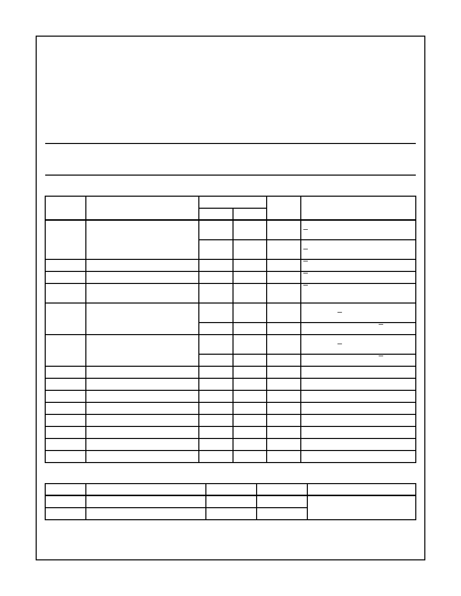
DC Electrical Specifications
V
CC
= 5V
±
10%; T
A
= -40
o
C to +85
o
C (HM-65262B-9, HM-65262-9, HM-65262C-9)
SYMBOL
PARAMETER
LIMITS
UNITS
TEST CONDITIONS
MIN
MAX
ICCSB1
Standby Supply Current
-od
50
µ
A
HM-65262B-9, HM-65262-9, IO = 0mA,
E = V
CC
-0.3V, V
CC
= 5.5V
-
900
µ
A
HM-65262C-9, IO = 0mA,
E = V
CC
-0.3V, V
CC
= 5.5V
ICCSB
Standby Supply Current
-
5
mA
E = 2.2V, IO = 0mA, V
CC
= 5.5V
ICCEN
Enabled Supply Current
-
50
mA
E = 0.8V, IO = 0mA, V
CC
= 5.5V
ICCOP
Operating Supply Current (Note 1)
-
50
mA
E = 0.8V, IO = 0mA, f = 1MHz,
V
CC
= 5.5V
ICCDR
Data Retention Supply Current
-
20
µ
A
HM-65262B-9, HM-65262-9,
V
CC
= 2.0V, E = V
CC
-
400
µ
A
HM-65262C-9, V
CC
= 2.0V, E = V
CC
ICCDR1
Data Retention Supply Current
-
30
µ
A
HM-65262B-9, HM-65262-9,
V
CC
= 3.0V, E = V
CC
-
550
µ
A
HM-65262C-9, V
CC
= 3.0V, E = V
CC
VCCDR
Data Retention Supply Voltage
2.0
-
V
II
Input Leakage Current
-1.0
+1.0
µ
A
VI = V
CC
or GND, V
CC
= 5.5V
IOZ
Output Leakage Current
-1.0
+1.0
µ
A
VIO = V
CC
or GND, V
CC
= 5.5V
VIL
Input Low Voltage
-0.3
0.8
V
V
CC
= 4.5V
VIH
Input High Voltage
2.2
V
CC
+0.3
V
V
CC
= 5.5V
VOL
Output Low Voltage
-
0.4
V
IO = 8.0mA, V
CC
= 4.5V
VOH1
Output High Voltage
2.4
-
V
IO = -4.0mA, V
CC
= 4.5V
VOH2
Output High Voltage (Note 2)
V
CC
-0.4
-
V
IO = -100
µ
A, V
CC
= 4.5V
Capacitance
T
A
= +25
o
C
SYMBOL
PARAMETER
MAX
UNITS
TEST CONDITIONS
CI
Input Capacitance (Note 2)
10
pF
f = 1MHz, All measurements are
referenced to device GND
CIO
Input/Output Capacitance (Note 2)
12
pF
NOTES:
1. Typical derating 5mA/MHz increase in ICCOP.
2. Tested at initial design and after major design changes.
HM-65262
6-4
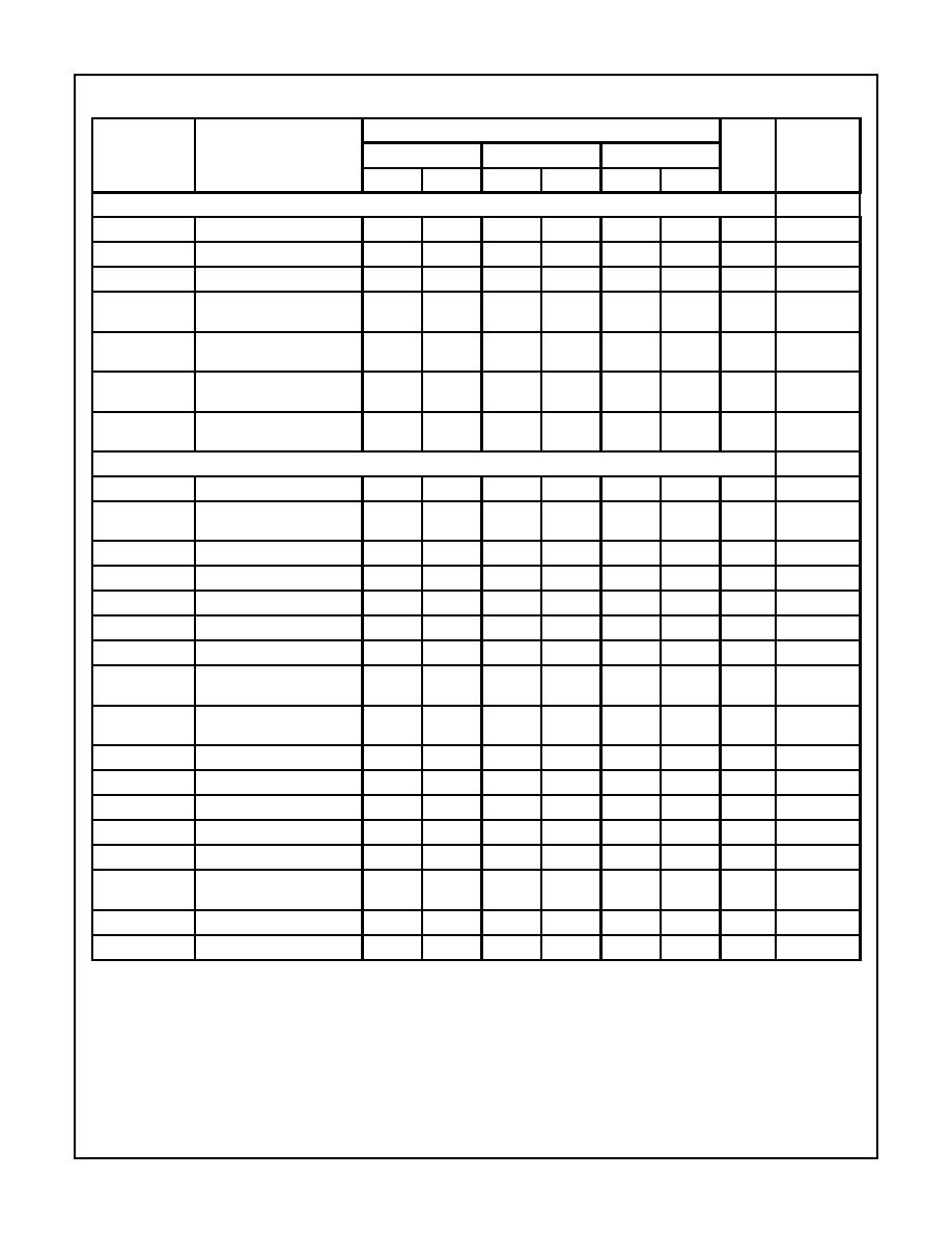
AC Electrical Specifications
V
CC
= 5V 10%,T
A
= -40
o
C to +85
o
C (HM-65262B-9, HM-65262-9, HM-65262C-9)
SYMBOL
PARAMETER
LIMITS
UNITS
TEST
CONDITIONS
HM-65262B-9
HM-65262-9
HM-65262C-9
MIN
MAX
MIN
MAX
MIN
MAX
READ CYCLE
(1)
TAVAX
Read/Cycle Time
70
-
85
-
85
-
ns
(Notes 1, 3)
(2)
TAVQV
Address Access Time
-
70
-
85
-
85
ns
(Notes 1, 3)
(3)
TELQV
Chip Enable Access Time
-
70
-
85
-
85
ns
(Notes 1, 3)
(4)
TELQX
Chip Enable Output Enable
Time
5
-
5
-
5
-
ns
(Notes 2, 3)
(5)
TEHQX
Chip Disable Output Hold
Time
5
-
5
-
5
-
ns
(Notes 2, 3)
(6)
TAXQX
Address Invalid Output Hold
Time
5
-
5
-
5
-
ns
(Notes 2, 3)
(7)
TEHQZ
Chip Enable Output Disable
Time
-
30
-
30
-
30
ns
(Notes 2, 3)
WRITE CYCLE
(8)
TAVAX
Write Cycle Time
70
-
85
-
85
-
ns
(Notes 1, 3)
(9)
TELWH
Chip Selection to End of
Write
55
-
65
-
65
-
ns
(Notes 1, 3)
(10)
TWLWH
Write Enable Pulse Width
40
-
45
-
45
-
ns
(Notes 1, 3)
(11)
TAVWL
Address Setup Time
0
-
0
-
0
-
ns
(Notes 1, 3)
(12)
TWHAX
Address Hold Time
0
-
0
-
0
-
ns
(Notes 1, 3)
(13)
TDVWH
Data Setup Time
30
-
35
-
35
-
ns
(Notes 1, 3)
(14)
TWHDX
Data Hold Time
0
-
0
-
0
-
ns
(Notes 1, 3)
(15)
TWLQZ
Write Enable Output Disable
Time
-
30
-
30
-
30
ns
(Notes 2, 3)
(16)
TWHQX
Write Disable Output Enable
Time
0
-
0
-
0
-
ns
(Notes 2, 3)
(17)
TAVWH
Address Valid to End of Write
55
-
65
-
65
-
ns
(Notes 1, 3)
(18)
TAVEL
Address Setup Time
0
-
0
-
0
-
ns
(Notes 1, 3)
(19)
TEHAX
Address Hold Time
0
-
0
-
0
-
ns
(Notes 1, 3)
(20)
TAVEH
Address Valid to End of Write
55
-
65
-
65
-
ns
(Notes 1, 3)
(21)
TELEH
Enable Pulse Width
55
-
65
-
65
-
ns
(Notes 1, 3)
(22)
TWLEH
Write Enable Pulse Setup
Time
40
-
45
-
45
-
ns
(Notes 1, 3)
(23)
TDVEH
Chip Setup Time
30
-
35
-
35
0
ns
(Notes 1, 3)
(24)
TEHDX
Data Hold Time
0
-
0
-
0
-
ns
(Notes 1, 3)
NOTES:
1. Input pulse levels: 0 to 3.0V; Input rise and fall times: 5ns (max); Input and output timing reference level: 1.5V; Output load: 1 TTL gate
equivalent and C
L
= 50pF (min) - for C
L
greater than 50pF, access time is derated by 0.15ns per pF.
2. Tested at initial design and after major design changes.
3. V
CC
= 4.5 and 5.5V.
HM-65262
6-5
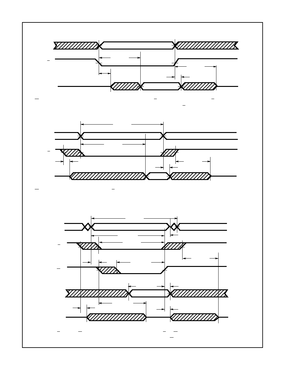
Timing Waveforms
NOTE:
1. W is high for entire cycle and D is ignored. Address is stable by the time E goes low and remains valid until E goes high.
FIGURE 1. READ CYCLE 1: CONTROLLED BY E
NOTE:
1. W is high for the entire cycle and D is ignored. E is stable prior to A becoming valid and after A becomes invalid.
FIGURE 2. READ CYCLE 2: CONTROLLED BY ADDRESS
NOTE:
1. In this mode, E rises after W. The address must remain stable whenever both E and W are low.
FIGURE 3. WRITE CYCLE 1: CONTROLLED BY W (LATE WRITE)
(4) TELQX
A
(3) TELQV
(5) TEHQX
(7) TEHQZ
E
Q
(1) TAVAX
(2) TAVQV
(4) TELQX
A
E
Q
(7) TEHQZ
(6) TAXQX
A
(17) TAVWH
(9) TELWH
(12) TWHAX
(10) TWLWH
(11)
(7) TEHQZ
(14) TWHDX
(13) TDVWH
(15) TWLQZ
(4)
TELQX
(16) TWHQX
(8) TAVAX
E
W
D
Q
TAVWL
HM-65262
6-6
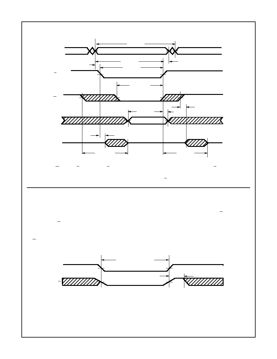
Low Voltage Data Retention
Intersil CMOS RAMs are designed with battery backup in
mind. Data retention voltage and supply current are guaran-
teed over temperature. The following rules ensure data
retention:
1. Chip Enable (E) must be held high during data retention;
within V
CC
to V
CC
+0.3V.
2. On RAMs which have selects or output enables (e.g., S,
G), one of the selects or output enables should be held in
the deselected state to keep the RAM outputs high
impedance, minimizing power dissipation.
3. Inputs which are to be held high (e.g., E) must be kept
between V
CC
+0.3V and 70% of V
CC
during the power
up and down transitions.
4. The RAM can begin operation > 55ns after V
CC
reaches
the minimum operating voltage (4.5V).
NOTE:
1. In this mode, W rises after E. If W falls before E by a time exceeding TWLQZ (Max) TELQX (Min), and rises after E by a time exceeding
TEHQZ (Max) TWHQZ (Min), then Q will remain in the high impedance state throughout the cycle.
FIGURE 4. WRITE CYCLE 2: CONTROLLED BY E (EARLY WRITE)
Timing Waveforms
(Continued)
(8) TAVAX
(20) TAVEH
E
W
D
Q
(21) TELEH
(22) TWLEH
(23) TDVEH
(19) TEHAX
(16) TWHQX
(24)
TEHDX
(4) TELQX
(15) TWLQZ
(7) TEHQZ
A
(18) TAVEL
V
CC
2.0V
4.5V
4.5V
V
CC
>55ns
V
CC
-0.3V TO V
CC
+0.3V
DATA RETENTION
MODE
E
FIGURE 5. DATA RETENTION TIMING
HM-65262
6-7
All Intersil semiconductor products are manufactured, assembled and tested under ISO9000 quality systems certification.
Intersil products are sold by description only. Intersil Corporation reserves the right to make changes in circuit design and/or specifications at any time without
notice. Accordingly, the reader is cautioned to verify that data sheets are current before placing orders. Information furnished by Intersil is believed to be accurate
and reliable. However, no responsibility is assumed by Intersil or its subsidiaries for its use; nor for any infringements of patents or other rights of third parties which
may result from its use. No license is granted by implication or otherwise under any patent or patent rights of Intersil or its subsidiaries.
For information regarding Intersil Corporation and its products, see web site http://www.intersil.com
Sales Office Headquarters
NORTH AMERICA
Intersil Corporation
P. O. Box 883, Mail Stop 53-204
Melbourne, FL 32902
TEL: (407) 724-7000
FAX: (407) 724-7240
EUROPE
Intersil SA
Mercure Center
100, Rue de la Fusee
1130 Brussels, Belgium
TEL: (32) 2.724.2111
FAX: (32) 2.724.22.05
ASIA
Intersil (Taiwan) Ltd.
Taiwan Limited
7F-6, No. 101 Fu Hsing North Road
Taipei, Taiwan
Republic of China
TEL: (886) 2 2716 9310
FAX: (886) 2 2715 3029
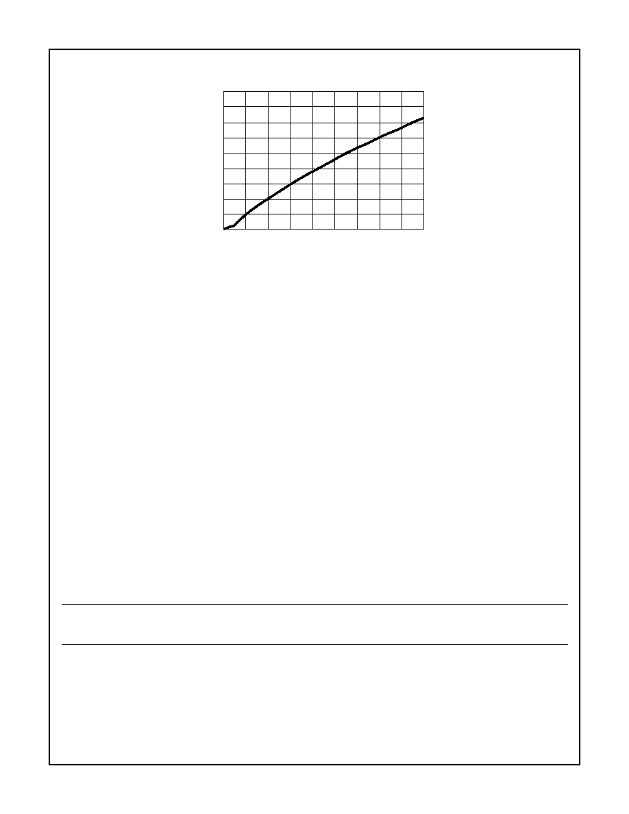
Typical Performance Curve
-55
-35
-15
5
25
45
65
85
105
125
-12
-11
-10
-9
-8
-7
-6
-5
-4
-3
V
CC
= 2.0V
LOGIC (I
CC
/(1A))
FIGURE 6. TYPICAL ICCDR vs T
A
T
A
(
o
C)
HM-65262