1
November 1997
ACS139MS
Radiation Hardened
Dual 2-to-4 Line Decoder/Demultiplexer
Features
∑ QML Qualified Per MIL-PRF-38535 Requirements
∑ 1.25Micron Radiation Hardened SOS CMOS
∑ Radiation Environment
- Latch-up Free Under any Conditions
- Total Dose . . . . . . . . . . . . . . . . . . . . . . 3 x 10
5
RAD(Si)
- SEU Immunity . . . . . . . . . . . <1 x 10
-10
Errors/Bit/Day
- SEU LET Threshold . . . . . . . . . . . >100MeV/(mg/cm
2
)
∑ Input Logic Levels . . .V
IL
= (0.3)(V
CC
), V
IH
= (0.7)(V
CC
)
∑ Output Current . . . . . . . . . . . . . . . . . . . . . . . . . . . .
±
8mA
∑ Quiescent Supply Current. . . . . . . . . . . . . . . . . . .400
µ
A
∑ Propagation Delay
- Enable to Output . . . . . . . . . . . . . . . . . . . . . . . . . 13ns
- Address to Output . . . . . . . . . . . . . . . . . . . . . . . . 15ns
Applications
∑ Memory Decoding
∑ Data Routing
∑ Code conversion
Description
The Radiation Hardened ACS139MS contains two indepen-
dent binary to one-of-four decoders, each with a single active
low enable input. Data on the select inputs cause one of the
four normally high outputs to go low.
If the enable input is high, all four outputs remain high. During
demultiplexer operation the enable input acts as the data input.
The enable input also functions as a chip select when the
devices are cascaded.
The ACS139MS is fabricated on a CMOS Silicon on Sapphire
(SOS) process, which provides an immunity to Single Event
Latch-up and the capability of highly reliable performance in
any radiation environment. These devices offer significant
power reduction and faster performance when compared to
ALSTTL types.
Specifications for Rad Hard QML devices are controlled
by the Defense Supply Center in Columbus (DSCC). The
SMD numbers listed below must be used when ordering.
Detailed Electrical Specifications for the ACS139 are
contained in SMD 5962-97639. A "hot-link" is provided
on our homepage with instructions for downloading.
http://www.semi.Intersil.com/data/sm/index.htm
Ordering Information
SMD PART NUMBER
INTERSIL PART NUMBER
TEMP. RANGE (
o
C)
PACKAGE
CASE OUTLINE
5962F9763901VEC
ACS139DMSR-02
-55 to 125
16 Ld SBDIP
CDIP2-T16
N/A
ACS139D/Sample-02
25
16 Ld SBDIP
CDIP2-T16
5962F9763901VXC
ACS139KMSR-02
-55 to 125
16 Ld Flatpack
CDFP4-F16
N/A
ACS139K/Sample-02
25
16 Ld Flatpack
CDFP4-F16
N/A
ACS139HMSR-02
25
Die
N/A
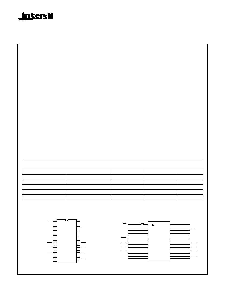
Pinouts
ACS139 (SBDIP)
TOP VIEW
ACS139 (FLATPACK)
TOP VIEW
14
15
16
9
13
12
11
10
1
2
3
4
5
7
6
8
1E
1A0
1A1
1Y0
1Y1
1Y2
GND
1Y3
V
CC
2A0
2A1
2Y0
2Y1
2Y2
2Y3
2E
1E
1A0
1A1
1Y0
1Y1
1Y2
1Y3
GND
2
3
4
5
6
7
8
1
16
15
14
13
12
11
10
9
V
CC
2E
2A0
2A1
2Y0
2Y1
2Y2
2Y3
File Number
4431
CAUTION: These devices are sensitive to electrostatic discharge; follow proper IC Handling Procedures.
http://www.intersil.com or 407-727-9207
|
Copyright
©
Intersil Corporation 1999
2
Die Characteristics
DIE DIMENSIONS:
Size: 2390
µ
m x 2390
µ
m (94 mils x 94 mils)
Thickness: 525
µ
m
±
25
µ
m (20.6 mils
±
1 mil)
Bond Pad: 110
µ
m x 110
µ
m (4.3 mils x 4.3 mils)
METALLIZATION:
Type: Al
Metal 1 Thickness: 0.7
µ
m
±
0.1
µ
m
Metal 2 Thickness: 1.0
µ
m
±
0.1
µ
m
SUBSTRATE:
Silicon on Sapphire (SOS)
SUBSTRATE POTENTIAL:
Unbiased Insulator
BACKSIDE FINISH:
Sapphire
PASSIVATION
Type: Phosphorous Silicon Glass (PSG)
Thickness: 1.30
µ
m
±
0.15
µ
m
SPECIAL INSTRUCTIONS:
Bond V
CC
First
ADDITIONAL INFORMATION:
Worst Case Density: <2.0 x 10
5
A/cm
2
Transistor Count: 190
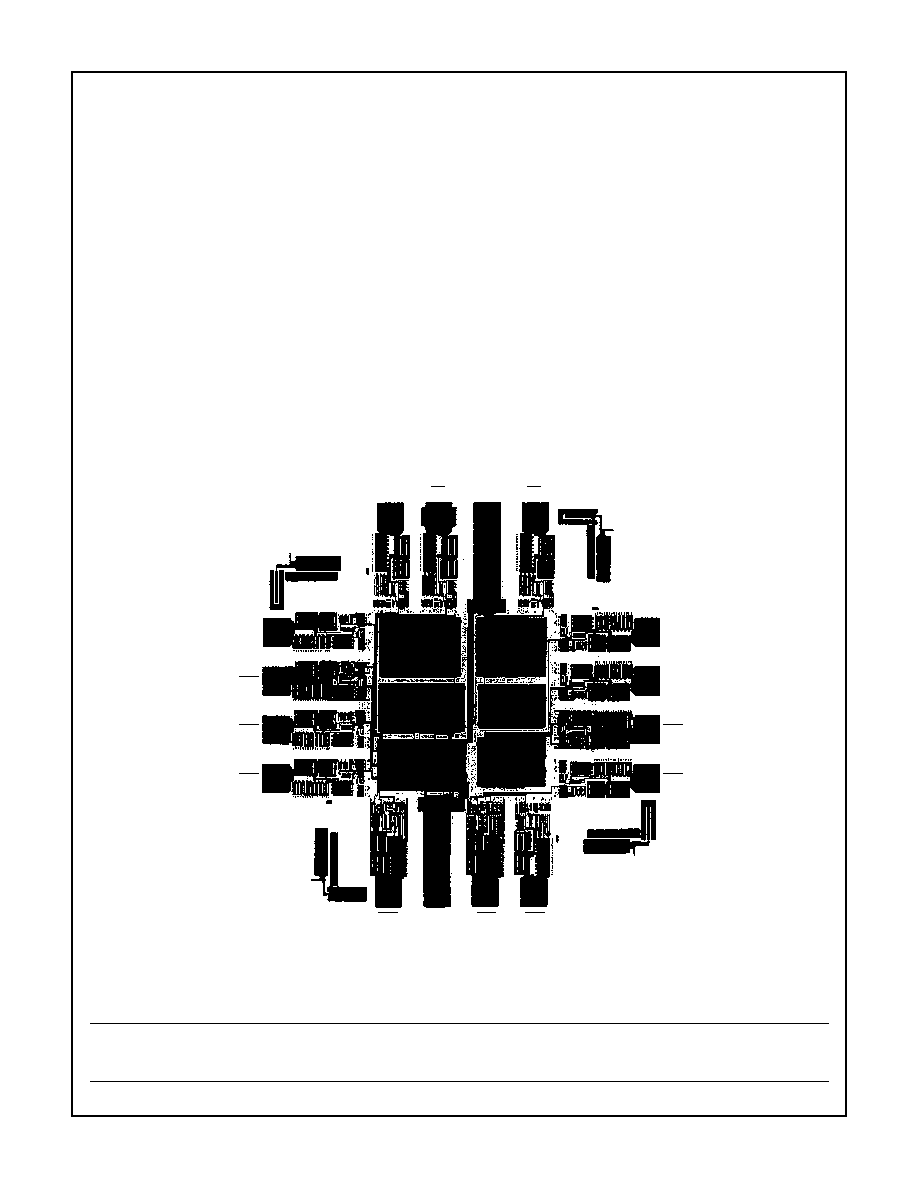
Metallization Mask Layout
ACS139MS.
1A0
1E
V
CC
2E
1A1
1Y0
1Y1
1Y2
2A0
2A1
2Y0
2Y1
1Y3
GND
2Y3
2Y2
ACS139MS
All Intersil semiconductor products are manufactured, assembled and tested under ISO9000 quality systems certification.
Intersil products are sold by description only. Intersil Corporation reserves the right to make changes in circuit design and/or specifications at any time without
notice. Accordingly, the reader is cautioned to verify that data sheets are current before placing orders. Information furnished by Intersil is believed to be accurate
and reliable. However, no responsibility is assumed by Intersil or its subsidiaries for its use; nor for any infringements of patents or other rights of third parties which
may result from its use. No license is granted by implication or otherwise under any patent or patent rights of Intersil or its subsidiaries.
For information regarding Intersil Corporation and its products, see web site http://www.intersil.com