1
CAUTION: These devices are sensitive to electrostatic discharge; follow proper IC Handling Procedures.
1-888-INTERSIL or 321-724-7143 | Copyright © Intersil Corporation 1999
TM
ACS630MS
Radiation Hardened EDAC
(Error Detection and Correction Circuit)
Features
∑ Devices QML Qualified in Accordance with MIL-PRF-38535
∑ Detailed Electrical and Screening Requirements are Contained in
SMD# 5962-96711 and Intersil' QM Plan
∑ 1.25 Micron Radiation Hardened SOS CMOS
∑ Total Dose . . . . . . . . . . . . . . . . . . . . . . . . . . . . . . . . >300K RAD (Si)
∑ Single Event Upset (SEU) Immunity: <1 x 10
-10
Errors/Bit/Day
(Typ)
∑ SEU LET Threshold . . . . . . . . . . . . . . . . . . . . . . . >100 MEV-cm
2
/mg
∑ Dose Rate Upset . . . . . . . . . . . . . . . . >10
11
RAD (Si)/s, 20ns Pulse
∑ Dose Rate Survivability . . . . . . . . . . . >10
12
RAD (Si)/s, 20ns Pulse
∑ Latch-Up Free Under Any Conditions
∑ Military Temperature Range . . . . . . . . . . . . . . . . . . -55
o
C to +125
o
C
∑ Significant Power Reduction Compared to ALSTTL Logic
∑ DC Operating Voltage Range . . . . . . . . . . . . . . . . . . . . 4.5V to 5.5V
∑ Input Logic Levels
- VIL = 30% of VCC Max
- VIH = 70% of VCC Min
∑ Input Current
1
µ
A at VOL, VOH
∑ Fast Propagation Delay . . . . . . . . . . . . . . . . 37ns (Max), 24ns (Typ)
Description
The Intersil ACS630MS is a Radiation Hardened 16-bit parallel error
detection and correction circuit. It uses a modified Hamming code to gen-
erate a 6-bit check word from each 16-bit data word. The check word is
stored with the data word during a memory write cycle; during a memory
read cycle a 22-bit word is taken form memory and checked for errors.
Single bit errors in the data words are flagged and corrected. Single bit
errors in check words are flagged but not corrected. The position of the
incorrect bit is pinpointed, in both cases, by the 6-bit error syndrome
code which is output during the error correction cycle.
The ACS630MS utilizes advanced CMOS/SOS technology to achieve
high-speed operation. This device is a member of a radiation hardened,
high-speed, CMOS/SOS Logic Family.
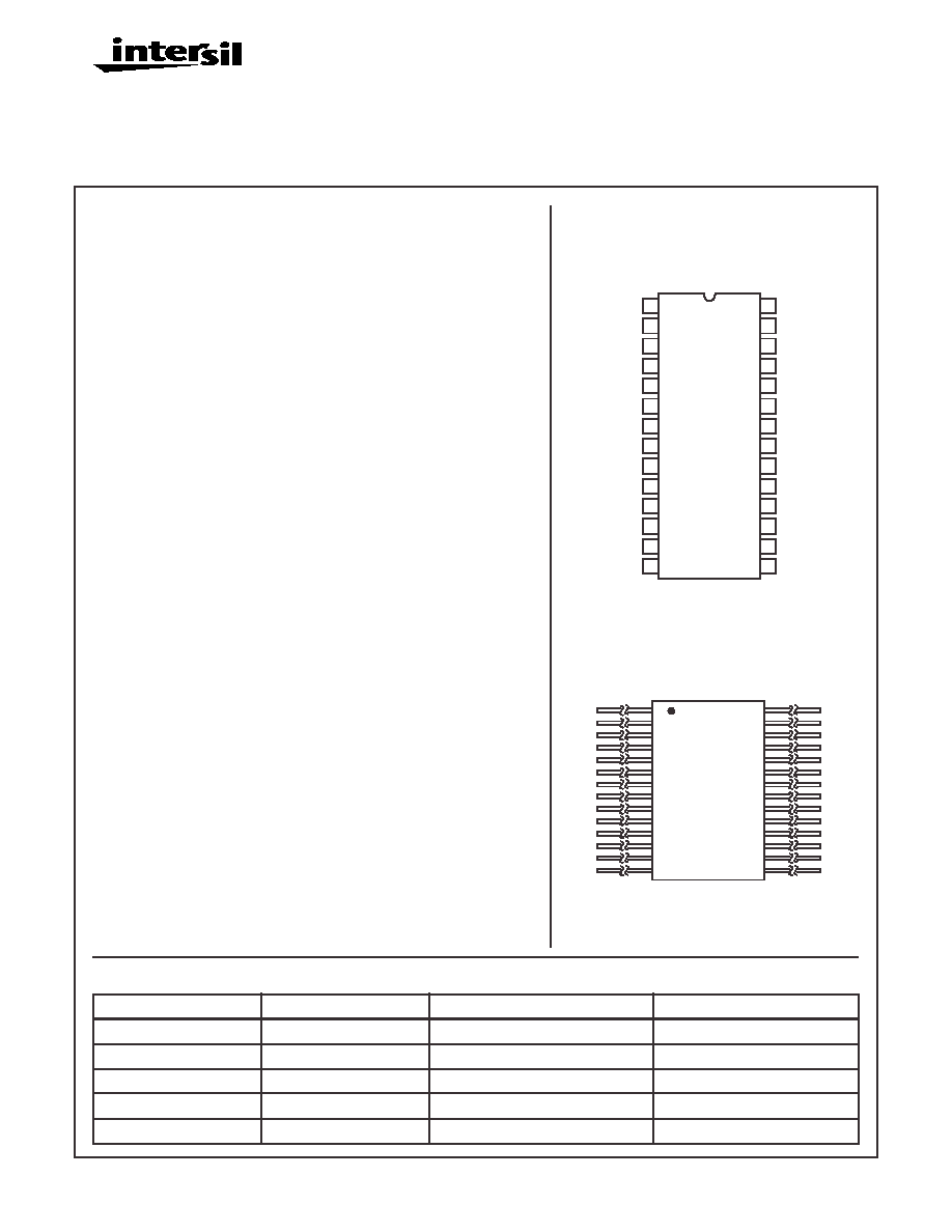
The ACS630MS is supplied in a 28 lead Ceramic Flatpack (K suffix) or a
28 Lead Ceramic Dual-In-Line Package (D suffix).
January 1996
Ordering Information
PART NUMBER
TEMPERATURE RANGE
SCREENING LEVEL
PACKAGE
5962F9671101VXC
-55
o
C to +125
o
C
MIL-PRF-38535 Class V
28 Lead SBDIP
5962F9671101VYC
-55
o
C to +125
o
C
MIL-PRF-38535 Class V
28 Lead Ceramic Flatpack
ACS630D/Sample
25
o
C
Sample
28 Lead SBDIP
ACS630K/Sample
25
o
C
Sample
28 Lead Ceramic Flatpack
ACS630HMSR
25
o
C
Die
Die
Pinouts
28 PIN CERAMIC DUAL-IN-LINE, MIL-STD-1835
DESIGNATOR CDIP2-T28, LEAD FINISH C
TOP VIEW
28 PIN CERAMIC FLATPACK, MIL-STD-1835
DESIGNATOR CDFP3-F28, LEAD FINISH C
TOP VIEW
DEF
DB0
DB1
DB2
DB3
DB4
DB5
DB6
DB7
DB8
DB9
DB10
DB11
GND
VCC
S1
S0
CB0
CB1
CB3
CB5
DB15
DB14
DB13
DB12
SEF
CB2
CB4
28
27
26
25
24
23
22
21
20
19
18
17
16
15
1
2
3
4
5
6
7
8
9
10
11
12
13
14
1
14
28
15
DEF
DB0
DB1
DB2
DB3
DB4
DB5
DB6
DB7
DB8
DB9
DB10
DB11
GND
VCC
SEF
S1
S0
CB0
CB1
CB2
CB3
CB4
CB5
DB15
DB14
DB13
DB12
2
3
4
5
6
7
8
9
10
11
12
13
27
26
25
24
23
22
21
20
19
18
17
16
Spec Number
518781
File Number
3199.1
itle
CS6
MS)
b-
t
adia-
n
rd-
ed
AC
rror
tec-
n
d
r-
-
n
r-
it))
thor
ey-
rds
nter-
rpo-
ion,
mi-
n-
ctor,
dia-
n
rd-
ed,
,
d