1
CAUTION: These devices are sensitive to electrostatic discharge; follow proper IC Handling Procedures.
1-888-INTERSIL or 321-724-7143 | Copyright © Intersil Corporation 1999
ACTS86MS
Radiation Hardened
Quad 2-Input Exclusive OR Gate
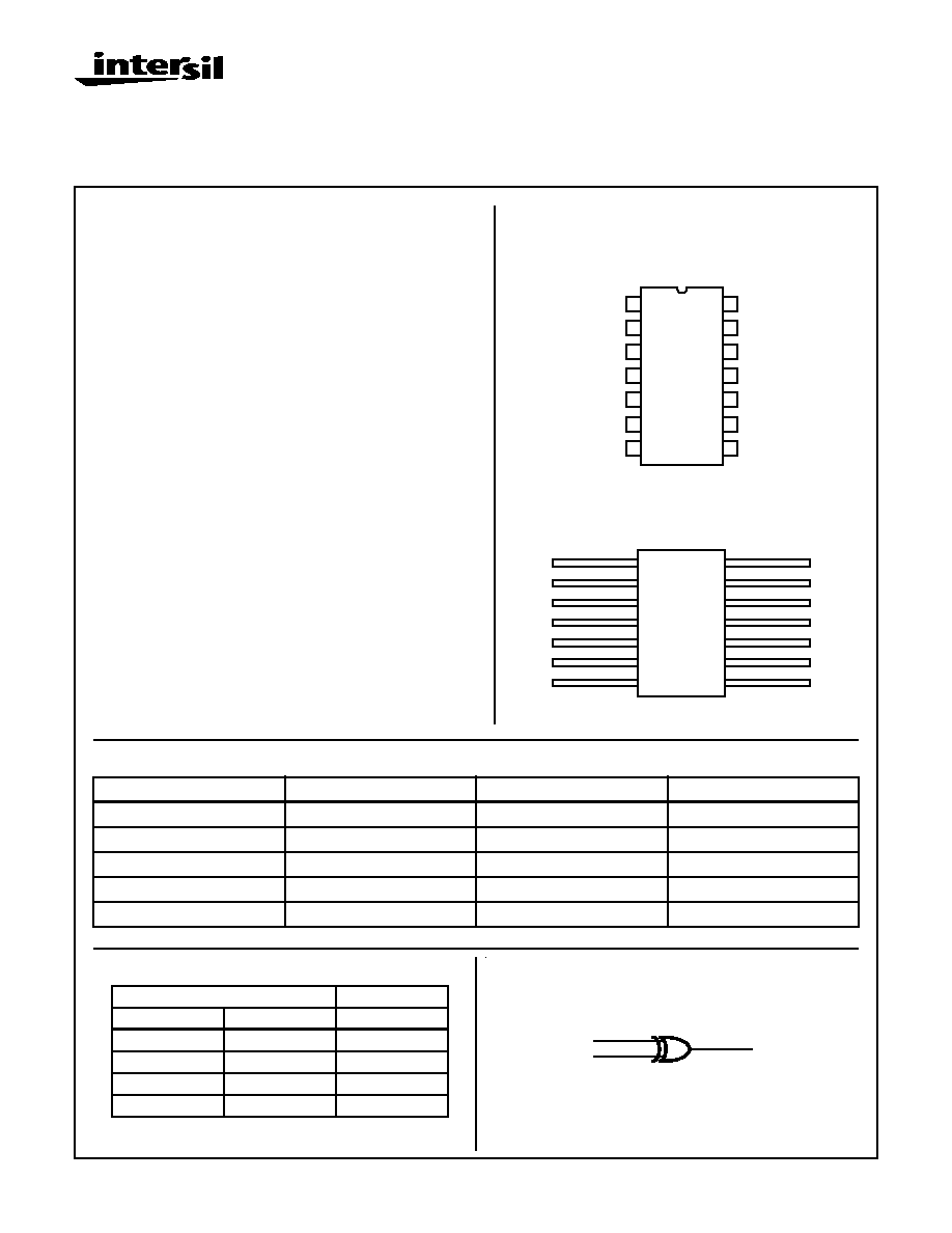
Pinouts
14 LEAD CERAMIC DUAL-IN-LINE
MIL-STD-1835 DESIGNATOR, CDIP2-T14, LEAD FINISH C
TOP VIEW
14 LEAD CERAMIC FLATPACK
MIL-STD-1835 DESIGNATOR, CDFP3-F14, LEAD FINISH C
TOP VIEW
A1
B1
Y1
A2
B2
Y2
GND
VCC
B4
A4
Y4
B3
A3
Y3
1
2
3
4
5
6
7
14
13
12
11
10
9
8
14
13
12
11
10
9
8
2
3
4
5
6
7
1
A1
B1
Y1
A2
B2
Y2
GND
VCC
B4
A4
Y4
B3
A3
Y3
April 1995
Truth Table
INPUTS
OUTPUT
An
Bn
Yn
L
L
L
L
H
H
H
L
H
H
H
L
NOTE: L = Logic Level Low, H = Logic Level High
Functional Diagram
An
Bn
(1, 4, 9, 12)
(2, 5, 10, 13)
Yn
(3, 6, 8, 11)
Features
∑ 1.25 Micron Radiation Hardened SOS CMOS
∑ Total Dose 300K RAD (Si)
∑ Single Event Upset (SEU) Immunity
<1 x 10
-10
Errors/Bit-Day (Typ)
∑ SEU LET Threshold >80 MEV-cm
2
/mg
∑ Dose Rate Upset >10
11
RAD (Si)/s, 20ns Pulse
∑ Latch-Up Free Under Any Conditions
∑ Military Temperature Range: -55
o
C to +125
o
C
∑ Significant Power Reduction Compared to ALSTTL Logic
∑ DC Operating Voltage Range: 4.5V to 5.5V
∑ Input Logic Levels
- VIL = 0.8V Max
- VIH = VCC/2V Min
∑ Input Current
1
µ
A at VOL, VOH
Description
The Intersil ACTS86MS is a radiation hardened quad 2-input
exclusive OR gate. A high logic level on any one input exclu-
sively will change the output to a high logic state.
The ACTS86MS utilizes advanced CMOS/SOS technology to
achieve high-speed operation. This device is a member of the
radiation hardened, high-speed, CMOS/SOS Logic Family.
Ordering Information
PART NUMBER
TEMPERATURE RANGE
SCREENING LEVEL
PACKAGE
ACTS86DMSR
-55
o
C to +125
o
C
Intersil Class S Equivalent
14 Lead SBDIP
ACTS86KMSR
-55
o
C to +125
o
C
Intersil Class S Equivalent
14 Lead Ceramic Flatpack
ACTS86D/Sample
+25
o
C
Sample
14 Lead SBDIP
ACTS86K/Sample
+25
o
C
Sample
14 Lead Ceramic Flatpack
ACTS86HMSR
+25
o
C
Die
Die
Spec Number
518847
File Number
3996
2
Specifications ACTS86MS
Absolute Maximum Ratings
Reliability Information
Supply Voltage . . . . . . . . . . . . . . . . . . . . . . . . . . . . . . -0.5V to +6.0V
Input Voltage Range . . . . . . . . . . . . . . . . . . . . . .-0.5V to VCC +0.5V
DC Input Current, Any One Input
. . . . . . . . . . . . . . . . . . . . . . . .±
10mA
DC Drain Current, Any One Output
. . . . . . . . . . . . . . . . . . . . . . .±
50mA
Storage Temperature Range (TSTG) . . . . . . . . . . . -65
o
C to +150
o
C
Lead Temperature (Soldering 10s) . . . . . . . . . . . . . . . . . . . . +265
o
C
Junction Temperature (TJ) . . . . . . . . . . . . . . . . . . . . . . . . . . +175
o
C
ESD Classification . . . . . . . . . . . . . . . . . . . . . . . . . . . . . . . . Class 1
(All Voltages Reference to VSS)
Thermal Impedance
JA
JC
DIP. . . . . . . . . . . . . . . . . . . . . . . . . . . . . .
74
o
C/W
24
o
C/W
Flat Pack . . . . . . . . . . . . . . . . . . . . . . . . .
116
o
C/W
30
o
C/W
Maximum Package Power Dissipation at +125
o
C
DIP. . . . . . . . . . . . . . . . . . . . . . . . . . . . . . . . . . . . . . . . . . . . . 0.7W
Flatpack . . . . . . . . . . . . . . . . . . . . . . . . . . . . . . . . . . . . . . . . . 0.4W
Maximum Device Power Dissipation . . . . . . . . . . . . . . . . . . .(TBD)W
Gate Count . . . . . . . . . . . . . . . . . . . . . . . . . . . . . . . . . . . . . 52 Gates
CAUTION: Stresses above those listed in "Absolute Maximum Ratings" may cause permanent damage to the device. This is a stress only rating and operation
of the device at these or any other conditions above those indicated in the operational sections of this specification is not implied.
Operating Conditions
Supply Voltage Range . . . . . . . . . . . . . . . . . . . . . . . +4.5V to +5.5V
Input Rise and Fall Time at 4.5V VCC (TR, TF) . . . . . . . 10ns/ V Max
Operating Temperature Range . . . . . . . . . . . . . . . . -55
o
C to +125
o
C
Input High Voltage (VIH) . . . . . . . . . . . . . . . . . . . . . . .VCC to VCC/2
Input Low Voltage (VIL). . . . . . . . . . . . . . . . . . . . . . . . . . . 0V to 0.8V
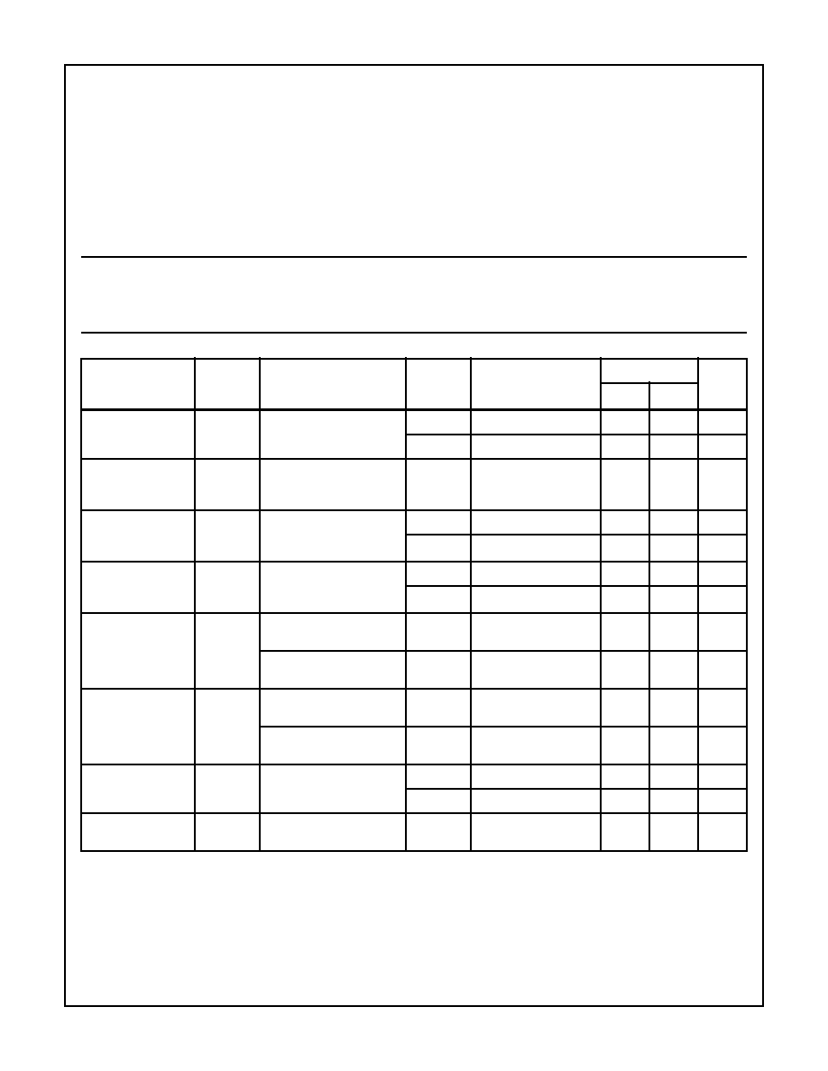
TABLE 1. DC ELECTRICAL PERFORMANCE CHARACTERISTICS
PARAMETER
SYMBOL
(NOTE 1)
CONDITIONS
GROUP
A SUB-
GROUPS
TEMPERATURE
LIMITS
UNITS
MIN
MAX
Supply Current
ICC
VCC = 5.5V,
VIN = VCC or GND
1
+25
o
C
-
5
µ
A
2, 3
+125
o
C, -55
o
C
-
100
µ
A
Delta ICC
DICC
VCC = 5.5V,
VIN = VCC or GND,
1 Input = 3.4V
1, 2, 3
+25
o
C, +125
o
C, -55
o
C
-
1.6
mA
Output Current
(Source)
IOH
VCC = VIH = 4.5V,
VOUT = VCC -0.4V,
VIL = 0V, (Note 2)
1
+25
o
C
-12
-
mA
2, 3
+125
o
C, -55
o
C
-8
-
mA
Output Current
(Sink)
IOL
VCC = VIH = 4.5V,
VOUT = 0.4V, VIL = 0V,
(Note 2)
1
+25
o
C
12
-
mA
2, 3
+125
o
C, -55
o
C
8
-
mA
Output Voltage High
VOH
VCC = 5.5V, VIH = 2.75V,
VIL = 0.8V, IOH = -50
µ
A
1, 2, 3
+25
o
C, +125
o
C, -55
o
C
VCC
-0.1
-
V
VCC = 4.5V, VIH = 2.25V,
VIL = 0.8V, IOH = -50
µ
A
1, 2, 3
+25
o
C, +125
o
C, -55
o
C
VCC
-0.1
-
V
Output Voltage Low
VOL
VCC = 5.5V, VIH = 2.75V,
VIL = 0.8V, IOH = 50
µ
A
1, 2, 3
+25
o
C, +125
o
C, -55
o
C
-
0.1
V
VCC = 4.5V, VIH = 2.25V,
VIL = 0.8V, IOH = 50
µ
A
1, 2, 3
+25
o
C, +125
o
C, -55
o
C
-
0.1
V
Input Leakage
Current
IIN
VCC = 5.5V,
VIN = VCC or GND
1
+25
o
C
-
±
0.5
µ
A
2, 3
+125
o
C, -55
o
C
-
±
1.0
µ
A
Noise Immunity
Functional Test
FN
VCC = 4.5V, VIH = 2.25V,
VIL = 0.8V, (Note 3)
7, 8A, 8B
+25
o
C, +125
o
C, -55
o
C
-
-
V
NOTES:
1. All voltages referenced to device GND.
2. Force/measure functions may be interchanged.
3. For functional tests, VO
4.0V is recognized as a logic "1", and VO
0.5V is recognized as a logic "0".
Spec Number
518847

3
Specifications ACTS86MS
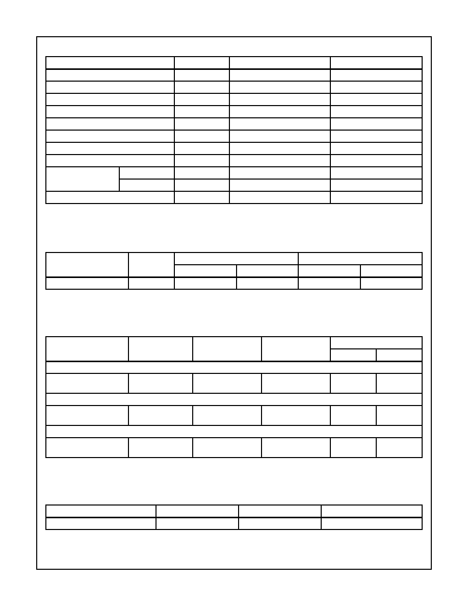
TABLE 2. AC ELECTRICAL PERFORMANCE CHARACTERISTICS
PARAMETER
SYMBOL
(NOTES 1, 2)
CONDITIONS
GROUP
A SUB-
GROUPS
TEMPERATURE
LIMITS
UNITS
MIN
MAX
Propagation Delay
Input to Output
TPHL
VCC = 4.5V, VIH = 3.0V,
VIL = 0V
9
+25
o
C
2
18
ns
10, 11
+125
o
C, -55
o
C
2
20
ns
TPLH
VCC = 4.5V, VIH = 3.0V,
VIL = 0V
9
+25
o
C
2
15
ns
10, 11
+125
o
C, -55
o
C
2
17
ns
NOTES:
1. All voltages referenced to device GND.
2. AC measurements assume RL = 500
, CL = 50pF, Input TR = TF = 3ns.
TABLE 3. ELECTRICAL PERFORMANCE CHARACTERISTICS
PARAMETER
SYMBOL
CONDITIONS
NOTE
TEMP
LIMITS
UNITS
MIN
TYP
MAX
Capacitance Power
Dissipation
CPD
VCC = 5.0V, VIH = 5.0V,
VIL = 0V, f = 1MHz
1
+25
o
C
-
25
-
pF
1
+125
o
C
-
25
-
pF
Input Capacitance
CIN
VCC = 5.0V, VIH = 5.0V,
VIL = 0V, f = 1MHz
1
+25
o
C
-
-
10
pF
1
+125
o
C
-
-
10
pF
NOTE:
1. The parameters listed in Table 3 are controlled via design or process parameters. Min and Max Limits are guaranteed but not directly
tested. These parameters are characterized upon initial design release and upon design changes which affect these characteristics.
TABLE 4. POST IRRADIATION ELECTRICAL PERFORMANCE CHARACTERISTICS
PARAMETER
SYMBOL
(NOTE 1)
CONDITIONS
TEMPERATURE
RAD LIMITS
UNITS
MIN
MAX
Supply Current
ICC
VCC = 5.5V, VIN = VCC or GND
+25
o
C
-
100
µ
A
Delta ICC
DICC
VCC = 5.5V, VIN = VCC or GND,
1 Input = 3.4V
+25
o
C
-
1.6
mA
Output Current
(Source)
IOH
VCC = VIH = 4.5V,
VOUT = VCC -0.4V, VIL = 0
+25
o
C
-8.0
-
mA
Output Current (Sink)
IOL
VCC = VIH = 4.5V,
VOUT = 0.4V, VIL = 0
+25
o
C
8.0
-
mA
Output Voltage High
VOH
VCC = 5.5V, VIH = 2.75V,
VIL = 0.8V, IOH = -50
µ
A
+25
o
C
VCC -0.1
-
V
VCC = 4.5V, VIH = 2.25V,
VIL = 0.8V, IOH = 50
µ
A
+25
o
C
VCC -0.1
-
V
Output Voltage Low
VOL
VCC = 5.5V, VIH = 2.75V,
VIL = 0.8V, IOH = 50
µ
A
+25
o
C
-
0.1
V
VCC = 4.5V, VIH = 2.25V,
VIL = 0.8V, IOH = 50
µ
A
+25
o
C
-
0.1
V
Input Leakage Current
IIN
VCC = 5.5V, VIN = VCC or GND
+25
o
C
-
±
1
µ
A
Noise Immunity
Functional Test
FN
VCC = 4.5V, VIH = 2.25V,
VIL = 0.8V, (Note 2)
+25
o
C
-
-
V
Propagation Delay
Input to Output
TPHL
VCC = 4.5V, VIH = 3.0V, VIL = 0V
+25
o
C
2
20
ns
TPLH
VCC = 4.5V, VIH = 3.0V, VIL = 0V
+25
o
C
2
17
ns
NOTES:
1. All voltages referenced to device GND.
2. For functional tests, VO
4.0V is recognized as a logic "1", and VO
0.5V is recognized as a logic "0".
TABLE 5. DELTA PARAMETERS (+25
o
C)
PARAMETER
SYMBOL
(NOTE 1)
DELTA LIMIT
UNITS
Supply Current
ICC
±
1.0
µ
A
Output Current
IOL/IOH
±
15
%
NOTE:
1. All delta calculations are referenced to 0 hour readings or pre-life readings.
Spec Number
518847
4
TABLE 6. APPLICABLE SUBGROUPS
CONFORMANCE GROUP
METHOD
GROUP A SUBGROUPS
READ AND RECORD
Initial Test (Preburn-In)
100%/5004
1, 7, 9
ICC, IOL/H
Interim Test 1 (Postburn-In)
100%/5004
1, 7, 9
ICC, IOL/H
Interim Test 2 (Postburn-In)
100%/5004
1, 7, 9
ICC, IOL/H
PDA
100%/5004
1, 7, 9, Deltas
Interim Test 3 (Postburn-In)
100%/5004
1, 7, 9
ICC, IOL/H
PDA
100%/5004
1, 7, 9, Deltas
Final Test
100%/5004
2, 3, 8A, 8B, 10, 11
Group A (Note 1)
Sample/5005
1, 2, 3, 7, 8A, 8B, 9, 10, 11
Group B
Subgroup B-5
Sample/5005
1, 2, 3, 7, 8A, 8B, 9, 10, 11, Deltas
Subgroups 1, 2, 3, 9, 10, 11
Subgroup B-6
Sample/5005
1, 7, 9
Group D
Sample/5005
1, 7, 9
NOTE:
1. Alternate Group A testing may be exercised in accordance with MIL-STD-883, Method 5005.
TABLE 7. TOTAL DOSE IRRADIATION
CONFORMANCE GROUP
METHOD
TEST
READ AND RECORD
PRE RAD
POST RAD
PRE RAD
POST RAD
Group E Subgroup 2
5005
1, 7, 9
Table 4
1, 9
Table 4 (Note 1)
NOTE:
1. Except FN test which will be performed 100% Go/No-Go.
TABLE 8. BURN-IN TEST CONNECTIONS (+125
o
C < TA < 139
o
C)
OPEN
GROUND
1/2 VCC = 3V
±
0.5V
VCC = 6V
±
0.5V
OSCILLATOR
50kHz
25kHz
STATIC BURN-IN 1 (Note 1)
-
1, 2, 4, 5, 7, 9, 10,
12, 13
3, 6, 8, 11
14
-
-
STATIC BURN-IN 2 (Note 1)
-
7
3, 6, 8, 11
1, 2, 4, 5, 9,
10, 12, 13, 14
-
-
DYNAMIC BURN-IN (Note 1)
-
7
3, 6, 8, 11
14
1, 2, 4, 5, 9,
10, 12, 13
-
NOTE:
1. Each pin except VCC and GND will have a series resistor of 500
±
5%.
TABLE 9. IRRADIATION TEST CONNECTIONS (TA = +25
o
C,
±
5
o
C)
FUNCTION
OPEN
GROUND
VCC
±
0.5V
Irradiation Circuit (Note 1)
3, 6, 8, 11
7
1, 2, 4, 5, 9, 10, 12, 13, 14
NOTE:
1. Each pin except VCC and GND will have a series resistor of 47k
±
5%. Group E, Subgroup 2, sample size is 4 dice/wafer, 0 failures.
Specifications ACTS86MS
Spec Number
518847

5
Specifications ACTS86MS
Spec Number
518847
Propagation Delay Timing Diagram and Load Circuit
Intersil - Space Products MS Screening
Wafer Lot Acceptance (All Lots) Method 5007 (Includes SEM)
Radiation Verification (Each Wafer) Method 1019,
4 Samples/Wafer, 0 Rejects
100% Nondestructive Bond Pull Method 2023
100% Internal Visual Inspection Method 2010
100% Temperature Cycling Method 1010 Condition C
(-65
o
to +150
o
C)
100% Constant Acceleration
100% PIND Testing
100% External Visual Inspection
100% Serialization
100% Initial Electrical Test
100% Static Burn-In 1 Method 1015, 24 Hours at +125
o
C Min
100% Interim Electrical Test 1 (Note 1)
100% Static Burn-In 2 Method 1015, 24 Hours at +125
o
C Min
100% Interim Electrical Test 2 (Note 1)
100% Dynamic Burn-In Method 1015, 240 Hours at +125
o
C
or 180 Hours at +135
o
C
100% Interim Electrical Test 3 (Note 1)
100% Final Electrical Test
100% Fine and Gross Seal Method 1014
100% Radiographics Method 2012 (2 Views)
100% External Visual Method 2009
Group A (All Tests) Method 5005 (Class S)
Group B (Optional) Method 5005 (Class S) (Note 2)
Group D (Optional) Method 5005 (Class S) (Note 2)
CSI and/or GSI (Optional) (Note 2)
Data Package Generation (Note 3)
NOTES:
1. Failures from interim electrical tests 1 and 2 are combined for determining PDA (PDA = 5% for subgroups 1, 7, 9 and delta failures com-
bined, PDA = 3% for subgroup 7 failures). Interim electrical tests 3 PDA (PDA = 5% for subgroups 1, 7, 9 and delta failures combined,
PDA = 3% for subgroup 7 failures).
2. These steps are optional, and should be listed on the purchase order if required.
3. Data Package Contents:
Cover Sheet (P.O. Number, Customer Number, Lot Date Code, Intersil Number, Lot Number, Quantity).
Certificate of Conformance (as found on shipper).
Lot Serial Number Sheet (Good Unit(s) Serial Number and Lot Number).
Variables Data (All Read, Record, and delta operations).
Group A Attributes Data Summary.
Wafer Lot Acceptance Report (Method 5007) to include reproductions of SEM photos. NOTE: SEM photos to include percent of step coverage.
X-Ray Report and Film, including penetrometer measurements.
GAMMA Radiation Report with initial shipment of devices from the same wafer lot; containing a Cover Page, Disposition, RAD Dose,
Lot Number, Test Package, Spec Number(s), Test Equipment, etc. Irradiation Read and Record data will be on file at Intersil.
VS
INPUT
OUTPUT
VIH
VSS
VOH
VOL
TPLH
TPHL
VS
AC VOLTAGE LEVELS
PARAMETER
ACTS
UNITS
VCC
4.50
V
VIH
4.50
V
VS
2.25
V
VIL
0
V
GND
0
V
DUT
TEST
CL
RL
POINT
50pF
500

6
ACTS86MS
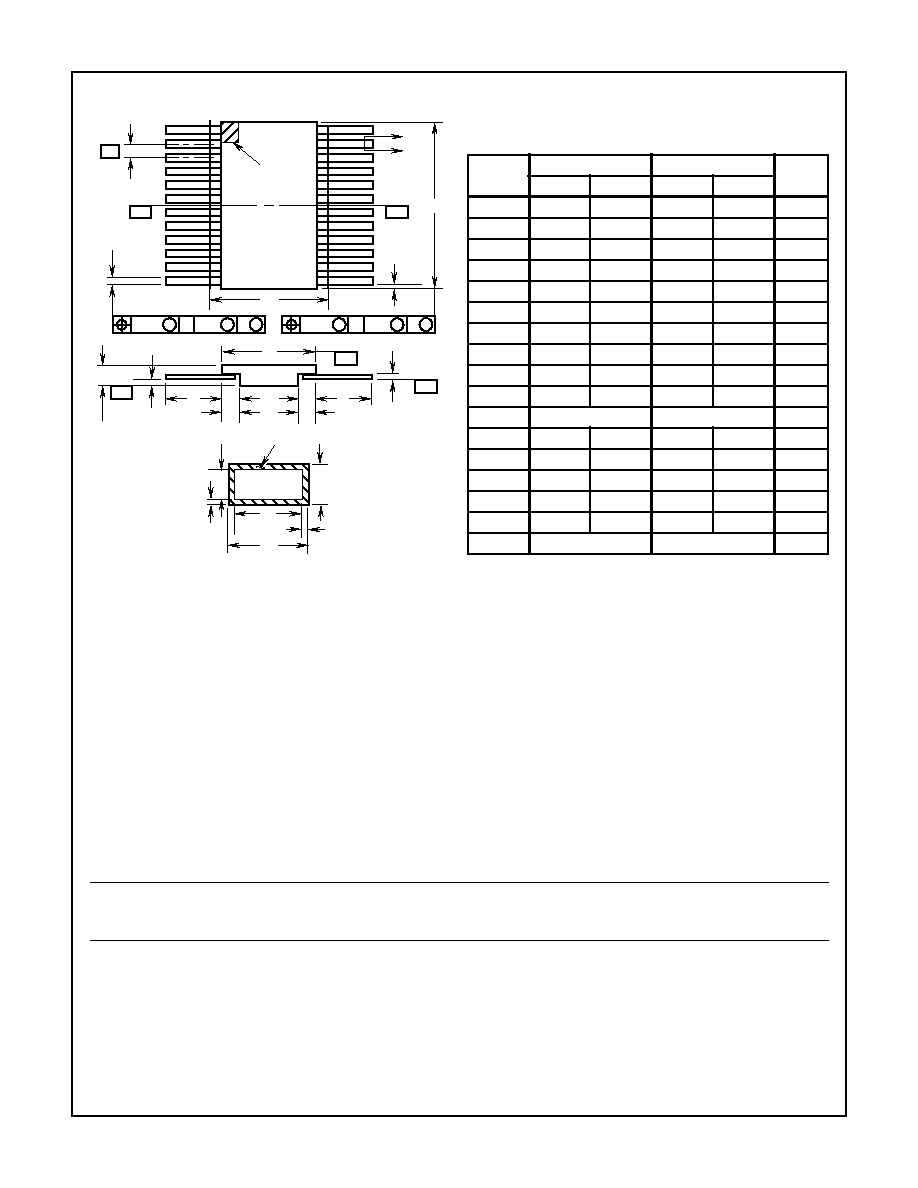
Metallization Mask Layout
ACTS86MS
(2)
(1)
(13)
GND
Y3
Y2
Y1 (3)
A2 (4)
NC
B2 (5)
(12) A4
(11) Y4
NC
A1
B4
B1
(6)
(7)
(8)
(10) B3
(14)
VCC
A3
(9)
Spec Number
518847
Die Characteristics
DIE DIMENSIONS:
88 mils x 88 mils
2.24mm x 2.24mm
METALLIZATION:
Type: AlSiCu
Metal 1 Thickness: 6.75k
≈
(Min), 8.25k
≈
(Max)
Metal 2 Thickness: 9k
≈
(Min), 11k
≈
(Max)
GLASSIVATION:
Type: SiO
2
Thickness: 8k
≈
±
1k
≈
DIE ATTACH:
Material: Silver Glass or JM7000 Polymer after 7/1/95
WORST CASE CURRENT DENSITY:
< 2.0 x 10
5
A/cm
2
BOND PAD SIZE:
> 4.3 mils x 4.3 mils
> 110
µ
m x 110
µ
m

7
ACTS86MS
Spec Number
518847
D14.3
MIL-STD-1835 CDIP2-T14 (D-1, CONFIGURATION C)
14 LEAD CERAMIC DUAL-IN-LINE METAL SEAL PACKAGE
SYMBOL
INCHES
MILLIMETERS
NOTES
MIN
MAX
MIN
MAX
A
-
0.200
-
5.08
-
b
0.014
0.026
0.36
0.66
2
b1
0.014
0.023
0.36
0.58
3
b2
0.045
0.065
1.14
1.65
-
b3
0.023
0.045
0.58
1.14
4
c
0.008
0.018
0.20
0.46
2
c1
0.008
0.015
0.20
0.38
3
D
-
0.785
-
19.94
-
E
0.220
0.310
5.59
7.87
-
e
0.100 BSC
2.54 BSC
-
eA
0.300 BSC
7.62 BSC
-
eA/2
0.150 BSC
3.81 BSC
-
L
0.125
0.200
3.18
5.08
-
Q
0.015
0.060
0.38
1.52
5
S1
0.005
-
0.13
-
6
S2
0.005
-
0.13
-
7
90
o
105
o
90
o
105
o
-
aaa
-
0.015
-
0.38
-
bbb
-
0.030
-
0.76
-
ccc
-
0.010
-
0.25
-
M
-
0.0015
-
0.038
2
N
14
14
8
Rev. 0 4/94
NOTES:
1. Index area: A notch or a pin one identification mark shall be locat-
ed adjacent to pin one and shall be located within the shaded
area shown. The manufacturer's identification shall not be used
as a pin one identification mark.
2. The maximum limits of lead dimensions b and c or M shall be
measured at the centroid of the finished lead surfaces, when
solder dip or tin plate lead finish is applied.
3. Dimensions b1 and c1 apply to lead base metal only. Dimension
M applies to lead plating and finish thickness.
4. Corner leads (1, N, N/2, and N/2+1) may be configured with a
partial lead paddle. For this configuration dimension b3 replaces
dimension b2.
5. Dimension Q shall be measured from the seating plane to the
base plane.
6. Measure dimension S1 at all four corners.
7. Measure dimension S2 from the top of the ceramic body to the
nearest metallization or lead.
8. N is the maximum number of terminal positions.
9. Braze fillets shall be concave.
10. Dimensioning and tolerancing per ANSI Y14.5M - 1982.
11. Controlling dimension: INCH.
bbb
C A - B
S
c
Q
L
A
SEATING
BASE
D
PLANE
PLANE
S
S
-D-
-A-
-C-
e
A
-B-
aaa
C A - B
M
D
S
S
ccc
C A - B
M
D
S
S
D
E
S1
b2
b
A
e
M
c1
b1
(c)
(b)
SECTION A-A
BASE
LEAD FINISH
METAL
e
A/2
S2
M
A
Ceramic Dual-In-Line Metal Seal Packages (SBDIP)
8
All Intersil semiconductor products are manufactured, assembled and tested under ISO9000 quality systems certification.
Intersil products are sold by description only. Intersil Corporation reserves the right to make changes in circuit design and/or specifications at any time without
notice. Accordingly, the reader is cautioned to verify that data sheets are current before placing orders. Information furnished by Intersil is believed to be accurate
and reliable. However, no responsibility is assumed by Intersil or its subsidiaries for its use; nor for any infringements of patents or other rights of third parties which
may result from its use. No license is granted by implication or otherwise under any patent or patent rights of Intersil or its subsidiaries.
For information regarding Intersil Corporation and its products, see web site http://www.intersil.com
Sales Office Headquarters
NORTH AMERICA
Intersil Corporation
P. O. Box 883, Mail Stop 53-204
Melbourne, FL 32902
TEL: (321) 724-7000
FAX: (321) 724-7240
EUROPE
Intersil SA
Mercure Center
100, Rue de la Fusee
1130 Brussels, Belgium
TEL: (32) 2.724.2111
FAX: (32) 2.724.22.05
ASIA
Intersil (Taiwan) Ltd.
Taiwan Limited
7F-6, No. 101 Fu Hsing North Road
Taipei, Taiwan
Republic of China
TEL: (886) 2 2716 9310
FAX: (886) 2 2715 3029
ACTS86MS
Spec Number
518847
-D-
-C-
0.004
H A - B
M
D
S
S
-A-
-B-
0.036
H A - B
M
D
S
S
e
E
A
Q
L
D
A
E1
SEATING AND
L
E2
E3
E3
BASE PLANE
-H-
b
C
S1
M
c1
b1
(c)
(b)
SECTION A-A
BASE
LEAD FINISH
METAL
PIN NO. 1
ID AREA
A
M
K14.A
MIL-STD-1835 CDFP3-F14 (F-2A, CONFIGURATION B)
14 LEAD CERAMIC METAL SEAL FLATPACK PACKAGE
SYMBOL
INCHES
MILLIMETERS
NOTES
MIN
MAX
MIN
MAX
A
0.045
0.115
1.14
2.92
-
b
0.015
0.022
0.38
0.56
-
b1
0.015
0.019
0.38
0.48
-
c
0.004
0.009
0.10
0.23
-
c1
0.004
0.006
0.10
0.15
-
D
-
0.390
-
9.91
3
E
0.235
0.260
5.97
6.60
-
E1
-
0.290
-
7.11
3
E2
0.125
-
3.18
-
-
E3
0.030
-
0.76
-
7
e
0.050 BSC
1.27 BSC
-
k
0.008
0.015
0.20
0.38
2
L
0.270
0.370
6.86
9.40
-
Q
0.026
0.045
0.66
1.14
8
S1
0.005
-
0.13
-
6
M
-
0.0015
-
0.04
-
N
14
14
-
Rev. 0 5/18/94
Ceramic Metal Seal Flatpack Packages (Flatpack)
NOTES:
1. Index area: A notch or a pin one identification mark shall be locat-
ed adjacent to pin one and shall be located within the shaded
area shown. The manufacturer's identification shall not be used
as a pin one identification mark. Alternately, a tab (dimension k)
may be used to identify pin one.
2. If a pin one identification mark is used in addition to a tab, the lim-
its of dimension k do not apply.
3. This dimension allows for off-center lid, meniscus, and glass overrun.
4. Dimensions b1 and c1 apply to lead base metal only. Dimension
M applies to lead plating and finish thickness. The maximum lim-
its of lead dimensions b and c or M shall be measured at the cen-
troid of the finished lead surfaces, when solder dip or tin plate
lead finish is applied.
5. N is the maximum number of terminal positions.
6. Measure dimension S1 at all four corners.
7. For bottom-brazed lead packages, no organic or polymeric mate-
rials shall be molded to the bottom of the package to cover the
leads.
8. Dimension Q shall be measured at the point of exit (beyond the
meniscus) of the lead from the body. Dimension Q minimum
shall be reduced by 0.0015 inch (0.038mm) maximum when sol-
der dip lead finish is applied.
9. Dimensioning and tolerancing per ANSI Y14.5M - 1982.
10. Controlling dimension: INCH.