1
Æ
FN7481.1
CAUTION: These devices are sensitive to electrostatic discharge; follow proper IC Handling Procedures.
1-888-INTERSIL or 1-888-468-3774
|
Intersil (and design) is a registered trademark of Intersil Americas Inc.
Copyright Intersil Americas Inc. 2004, 2005. All Rights Reserved
All other trademarks mentioned are the property of their respective owners.
BBT3420
Quad 2.488-3.1875Gbps/Channel Transceiver
1 Features
∑ Four channels of transmitter and receiver with serial data
transfer rates of 2.488-3.1875Gbps/channel with full rate
and half-rate operations
∑ Up to 12.75Gbps data rate at full duplex
∑ User-controlled dual-speed operation (per channel) 2.488-
3.1875Gbps or 1.244-1.59Gbps
∑ IEEE 802.3ae-2002 10 GE and 10 GFC compliant
- XAUI, XGMII, and MDC/MDIO interfaces
∑ XGMII format 10-bit parallel input/output data
- Supports HSTL 1.8V and 2.5V SSTL_2
∑ Extensive configuration via 802.3-compliant MDC/MDIO
serial interface
∑ 8bit/10bit Encoding/Decoding per channel with selectable
parallel input/output data sizes
- Support optional 8b/10b encoder/decoder bypass
operation
∑ Integrated Equalization and Pre-emphasis
∑ De-skewing and channel-to-channel alignment options
∑ Low power, 250mW per channel typical
∑ Meets jitter requirements with significant margin
∑ Comma detection and synchronization, byte alignment
∑ Tx/Rx rate matching via IDLE insertion/deletion
∑ Receive signal detect and 16 levels of transmission
medium equalization
∑ CML transmit outputs with four levels of pre-emphasis
∑ Loopback
- Per-channel serial Tx-to-Rx and Rx-to-Tx parallel
internal loopback modes
∑ Single-ended/differential input Reference clock
∑ Double Data-Rate (DDR) mode, also optional SDR (Single
Data Rate) on transmitter
∑ Support both source-centered and source-simultaneous
clocking
∑ Long Run Length (512 bit) frequency lock ideal for
proprietary encoding schemes Transmit byte clock
schemes
- One Transmit Byte Clock (TBC) for each channel, or
one TBC for all four channels
∑ Received clock schemes
- Receive data aligned to local reference clock, to
recovered clock for each channel, or to recovered clock
for Channel A only
∑ Supports Built-In Self Test (BIST) and IEEE 1149.1 JTAG
∑ On-chip 25
series output terminations (XGMII side)
∑ Standard 0.18µm 1.8V CMOS technology
∑ 3.3V tolerant I/O
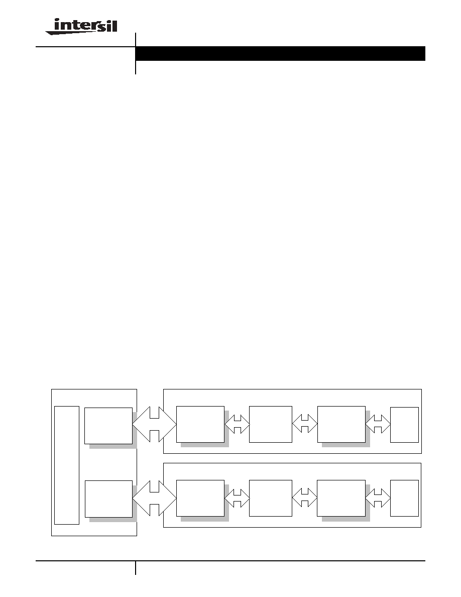
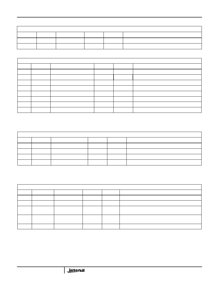
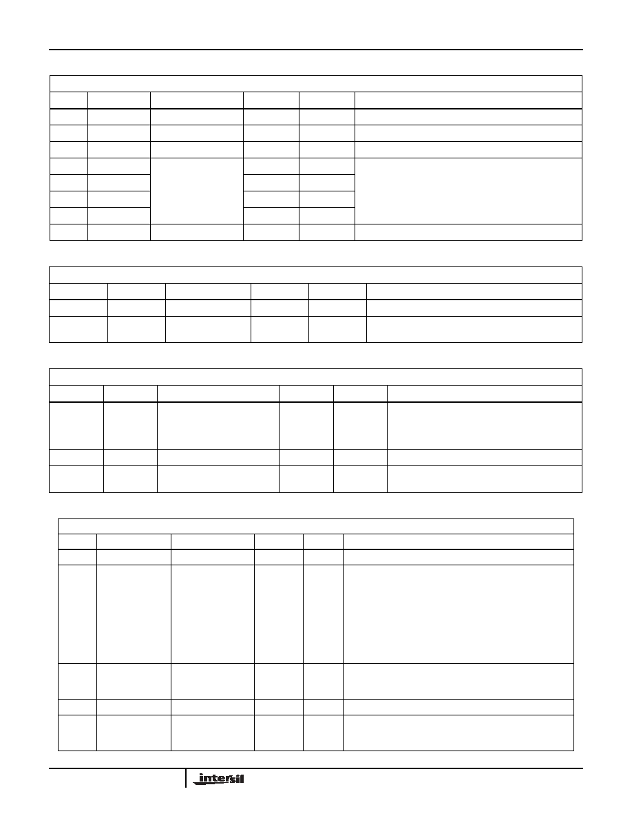
FIGURE 1-1. EXAMPLE BACKPLANE AND LINE CARD APPLICATIONS
Switch Card
Switch
Fabric
nPower BBT 3420
Transceiver
nPower BBT 3420
Transceiver
nPower BBT 3420
Transceiver
Serial 10 Gigabit
10GBASE-R
Custom ASIC
&
MAC Functions
XGMII
nPower BBT 3420
Transceiver
XAUI
XAUI
XGMII
XAUI
Up to 40"
Optical
Transponder
nPower BBT 3420
Transceiver
WDM 10 Gigabit
10GBASE-LX4
Custom ASIC
&
MAC Functions
XGMII
nPower BBT 3420
Transceiver
XAUI
XAUI
XGMII
XAUI
Up to 40"
WDM
Optical
Transponder
B
ackp
lan
e
In
ter
f
ace
Data Sheet
September 14, 2005
2
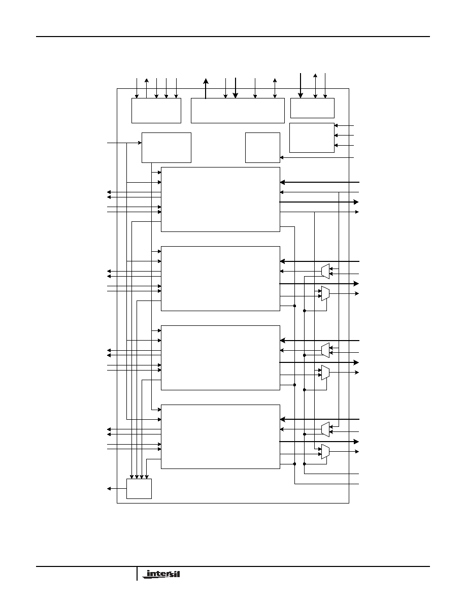
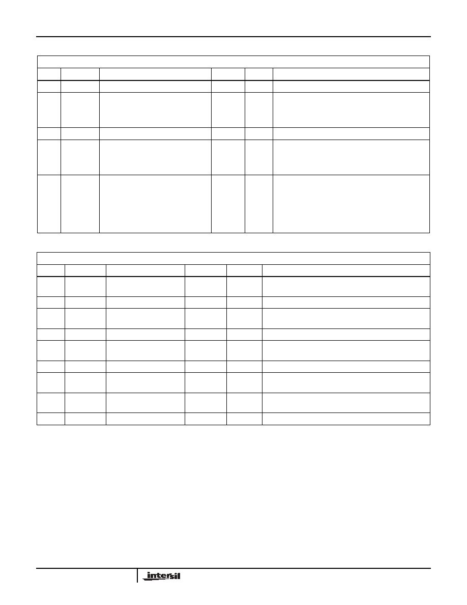
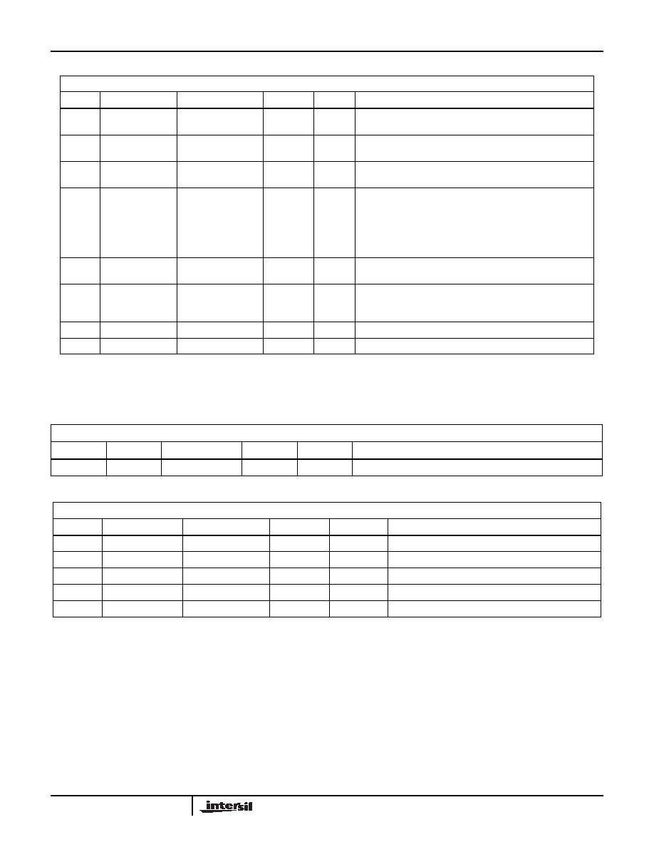
FIGURE 1-2. BBT3420 BLOCK DIAGRAM
SSTL or HSTL
Input
Reference
MDIO Protocol
Engine
MDIO Register File & Common Logic
JTAG
TAP
MD
I
O
MD
C
P
A
D
R
[
4:
0]
TDI
TDO
TM
S
TCL
K
TRST
N
20X or 10X
Transmit Clock
Generator
MF
[A:
D
]
RS
T
N
LP
EN[A:D
]
SIG_DET
BIST
EN
R
SVN
/
RE
T
I
M
E
R
VREF
REFP(N.C.)
REFN(N.C.)
RREF(N.C.)
Internal
Nodes
RFCP
RFCN
RFCN
Channel A
TD[9:0]
TBC
RD[9:0]
RBC
TX+
TX-
RX+
RX-
SIGDET
CODE
HS_TX_CLK
TXAP
TXAN
RXAP
RXAN
REF_CLK
TDA[9:0]
TCA
RDA[9:0]
RCA
RFCN
Channel B
TD[9:0]
TBC
RD[9:0]
RBC
TX+
TX-
RX+
RX-
SIGDET
CODE
HS_TX_CLK
TXBP
TXBN
RXBP
RXBN
REF_CLK
TDB[9:0]
TCB
RDB[9:0]
RCB
RFCN
Channel C
TD[9:0]
TBC
RD[9:0]
RBC
TX+
TX-
RX+
RX-
SIGDET
CODE
HS_TX_CLK
TXCP
TXCN
RXCP
RXCN
REF_CLK
TDC[9:0]
TCC
RDC[9:0]
RCC
RFCN
Channel D
TD[9:0]
TBC
RD[9:0]
RBC
TX+
TX-
RX+
RX-
SIGDET
CODE
HS_TX_CLK
TXDP
TXDN
RXDP
RXDN
REF_CLK
TDD[9:0]
TCD
RDD[9:0]
RCD
PSYNC
CODE
SIGNAL
DETECT
LOGIC
BBT3420
3
2 General Description
The BBT3420 is a quad 8-bit/10-bit parallel-to-serial and
serial-to-parallel transceiver device ideal for high-bandwidth
interconnection between line cards, serial backplanes, or
optical modules, over interconnect media such as Printed
Circuit Board (PCB) FR-4 traces or copper cables.
Each independent transceiver channel in BBT3420 is
capable of operating at 2.488-3.1875Gbps at full-rate, and
1.244-1.59375Gbps at half-rate. The four on-chip
transceivers shown in Figure 1-2 can also be configured as
a single 10 Gigabit Attachment Unit Interface (XAUI), for
both 10G Ethernet and 10G Fiber Channel or proprietary
backplane interfaces, providing up to 12.75Gbps of data
throughput at full duplex. The BBT3420 also supports the 10
Gigabit Media Independent Interface (XGMII) on the parallel
interfaces. The device can be used as an XGMII Extended
Sublayer (XGXS) device to support longer PCB traces
between optical transceiver modules and switch fabrics, as
shown in Figure 1-1.
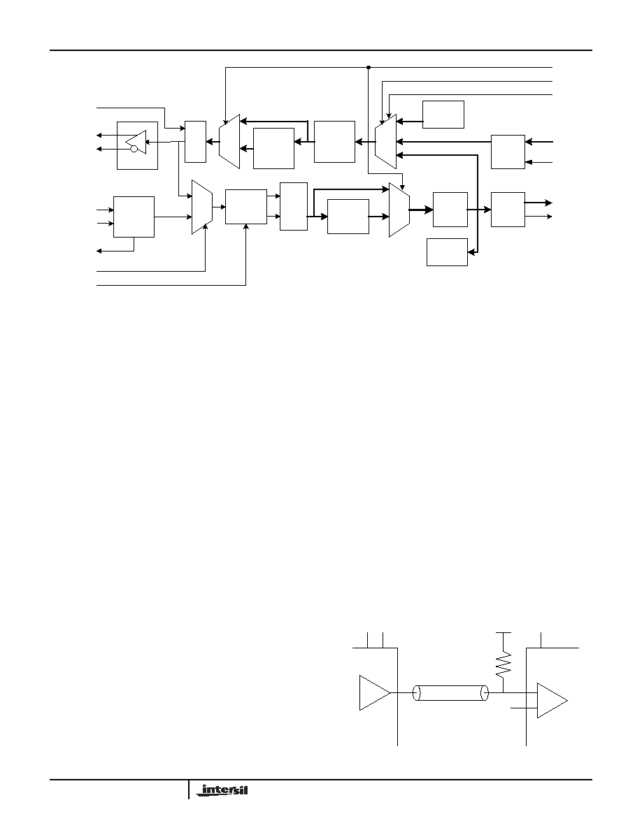
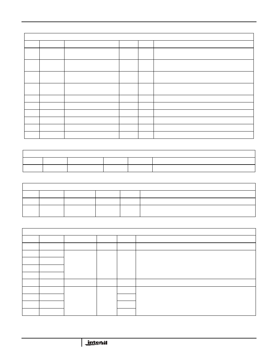
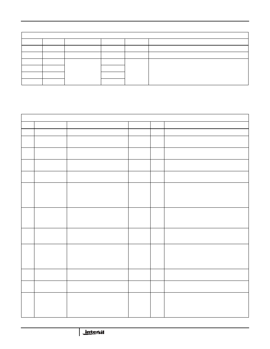
As shown in Figure 1-3, each transceiver channel in
BBT3420 contains a serializer, a deserializer, an 8b/10b
encoder and decoder, as well as elastic buffers that provide
the interface for serial data transmission and data recovery.
Both the receive equalization and the transmit pre-emphasis
are provided on each of the channels to maximize
performance. In addition, a programmable receive FIFO in
each channel aligns all incoming serial data to the local clock
domain, adding or removing IDLE sequences as needed.
This in return will eliminate the need for multiple clock
domains for the interfaced ASIC device to the transceiver.
Each transceiver channel can also be configured to operate
as a non-encoded 10-bit transceiver, allowing long strings of
consecutive 1's or 0's (up to 512 bits). This feature enables
the BBT3420 to accommodate proprietary encoded data
links.
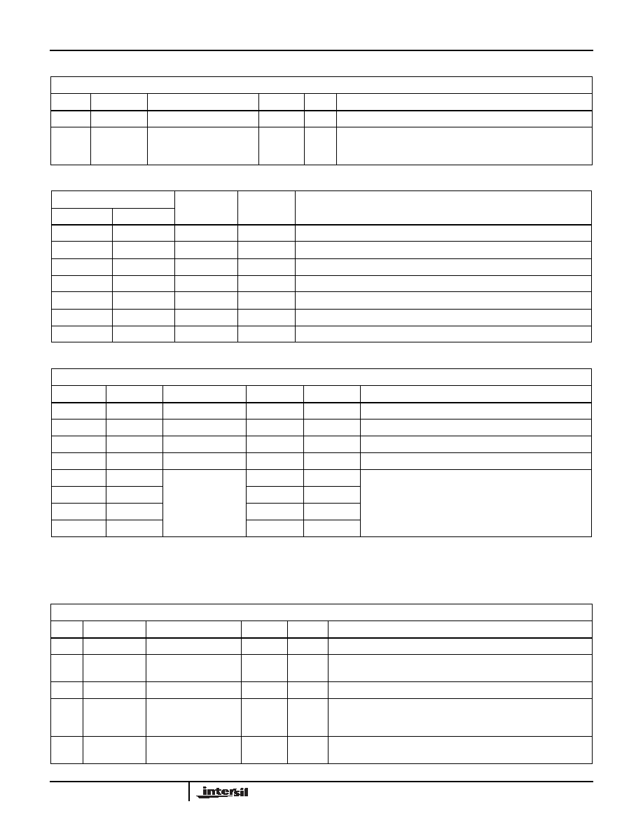
On each channel, the transmitter accepts up to 10-bit wide
parallel SSTL_2 or HSTL Class I/O (Figure 2-1) data, which
is then serialized into high-speed NRZ (Non-Return to Zero)
serial streams. The effective serial output impedance is
nominally 150
differential.
The BBT3420 transceiver can be configured via pins and
through the Management Data Input/Output (MDIO)
interface specified in IEEE 802.3 Clause 22 or Clause 45.
The device supports both the 5-bit PHY address for Clause
22 and the 5-bit port address for Clause 45. The four device
addresses for Clause 45 are user selectable. The device
also supports the Built-in Self Test (BIST) and IEEE 1149.1
(JTAG) for self-test purposes including serial and parallel
loopback under either external pin or MDIO control, and
Pseudo Random Bit Sequence (PRBS) generation and
verification.
The BBT3420 is assembled in a 289-pin 19mm x 19mm
HSBGA package. The device can operate with a single 1.8V
supply and dissipates only 250mW per channel.
FIGURE 1-3. FUNCTIONAL BLOCK DIAGRAM OF A SINGLE CHANNEL
Clock and
Data
Recovery
100 Ohm
Termination,
Equalizer,
Signal
Detect
De
se
ria
l
i
z
er &
Co
m
m
a
De
tecto
r
10B/8B
Decoder
RX FIFO
Deskew
Logic
Se
ri
al
izer
8B/10B
Encoder
&
AKR
Generator
TX FIFO
&
Error and
Orderset
Detector
BIST
Pattern
Generator
BIST
Pattern
Analyzer
DDR
Input
Registers
DDR
Output
Registers
TD[9:0]
TBC
RD[9:0]
RBC
TX+
TX-
RX+
RX-
SIGDET
CODE
HS_TX_CLK
REF_CLK
BISTEN
PLP
SLP
Pre-empahsis
FIGURE 2-1. SSTL_2/HSTL CLASS I I/O
VTT=VDDQ/2
50
Zo=50
VREF= VDDQ/2
VD
D
Q
/
2
VD
D
Q
VD
D
Q
BBT3420
4
3.0 Detailed Functional Description
3.1 Transmit Parallel Input Modes
The parallel side of each of the channels in BBT3420 may
operate in either a 10-bit mode or a XGMII 9-bit mode. The
parallel input mode selection is controlled by the CODE pin
(Table 4-6) and the CODECENA bit in the MDIO register at
address 11'h in Clause 22 format (Table 3-16) and/or C000'h
in Clause 45 format (Table 3-32). In order to program the
device for XGMII 9-bit mode, the CODE pin should be set
HIGH and the CODECENA bit set to 1'b. For the 10-bit
Mode setting, either the CODE pin should be set to LOW or
the CODECENA bit should be set to 0'b.
3.1.1 10-BIT MODE
In the 10-bit mode the 8b/10b Codec is disabled, and the
externally encoded data are latched in the DDR input
registers in increments of 10 bits. In this case, the user is
responsible for generating and applying the proper input in
the form of ordered sets, data, and correct `comma' group
signals, to ensure data coherence. The LSB (TDX[0]) is
shifted out first on the serial side, and the MSB (TDX[9]) is
shifted out last.
3.1.2 XGMII 9-BIT (8 BITS PLUS K CONTROL BIT) MODE
In the XGMII 9-bit mode, the unencoded data are latched in
the DDR input registers in 9 bits at a time. The lower 8 bits
(TD[A..D][7:0]) are byte-wide data or control values, and the
9
th
bit (TD[A..D][8]) is the "K" bit used to select special
control characters for link management. In this mode, the
10
th
bit (TD[A..D][9]) is used for disparity error or code
violation. The
8b/10b Codec is enabled, and converts the
data and the valid control values.
The XGMII IDLE Code Register (Clause 22 Address 1B'h or
Clause 45 Address C003'h) controls the data pattern that
represents an IDLE character. The default value of this
register is 07'h. The register can be programmed to any 8-bit
value excluding the already defined (control) values shown
in Table 3-1.
When both the TRANS_EN bit (Clause 22 Address 10'h in
Table 3-15 or Clause 45 Address C001'h in Table 3-33) and
the AKR_EN bit (Clause 22 Address 1D'h in Table 3-28 or
Clause 45 Address C001'h in Table 3-33) are set to 1, or
when the XAUI_EN bit is set, the IDLE character data
pattern will be sequenced into /A/, /K/, and /R/ codes (IEEE
802.3ae-2002 specified). Alternatively, if neither of the
AKR_EN or XAUI_EN bits are set, the XGMII IDLE and the
/K/ code will both be transmitted as the XAUI /K/ code, and
the /A/ and /R/ control codes will be transmitted as XAUI /A/
and /R/ codes respectively. The 8b/10b encoding patterns
are described in Table 3-1. For valid operation, the XGMII
and XAUI Lane 0 signals should be connected to the
BBT3420 Channel A pins.
When the XAUI_EN bit is set to 1, if a local/remote fault is
received on the XAUI inputs, it will be passed as ||LF|| or
||RF|| Sequence Ordered_sets respectively, i.e.,
/K28.4/D0.0/D0.0/D1.0(D2.0)/. Local fault is declared when
any of the following conditions are detected:
1. No signal is detected in any one of four channels.
2. No valid comma is detected in any one or more of the four
channels.
3. When all the channels are not deskewed.
When the XAUI_EN bit is set to 1, if a local/remote fault
K28.4/D0.0/D0.0/D1.0(D2.0)/ is written to the XGMII transmit
interface for XAUI transmission, the ||LF|| or ||RF|| Sequence
Ordered_set is transmitted according to the IEEE 802.3ae-
2002 randomizing algorithm. Any other Sequence
Ordered_set will also be transmitted in the same way.
TABLE 3-1. VALID 8B/10B ENCODER PATTERNS
TRANSMITTING SERDES
NOTES and
DESCRIPTION
K-BIT
TD DATA
TRANS_EN
BIT (Note 1)
AKR_EN BIT
(Note 1)
SERIAL
CHARACTER
SERIAL
CODE
0
0-FF'h
X
X
See 802.3-2002 Table36-1
Valid Data Value
1
= XGMII IDLE reg.
(Note 2) (default 07'h)
0
X
Invalid code
1
0
/K/
K28.5
Comma (Sync)
1
/A/ /K/ /R/
IEEE802.3ae 48.2.4.2 algorithm
1
BC
X
0
/K/
K28.5
Comma (Sync)
1
/A/ /K/ /R/
IEEE802.3ae 48.2.4.2 algorithm
1
7C
X
0
/A/
K28.3
Align
1
/A/ /K/ /R/
IEEE802.3ae 48.2.4.2 algorithm
1
1C
X
0
/R/
K28.0
Alternate Idle (Skip)
1
/A/ /K/ /R/
IEEE802.3ae 48.2.4.2 algorithm
1
FB
X
X
/S/
K27.7
Start
BBT3420
5
3.2 Transmit Byte Clock
3.2.1 FULL- AND HALF-RATE MODE
Since the BBT3420 normally employs Double Data Rate
(DDR) timing, the local reference clock requirement is
lowered to 124.4-159.375MHz. The Transmit Byte Clock
(TBC) must be frequency-synchronous with the local
reference clock. For any channel set to Half-Rate Clock
Mode by the MDIO/MDC register 1F'h (for Clause 22) and/or
C008'h (for Clause 45), see Table 3-30, the TBC must be
provided at half the ref clock frequency, unless the TX_SDR
bit is set in the MDIO register C001'h (Clause 45, Table 3-
33) and/or 1D'h (Clause 22, Table 3-28).
3.2.2 SOURCE-CENTERED AND -SIMULTANEOUS
MODE
For ease of ASIC timing, the BBT3420 provides the option
for the TBC to be source-simultaneous or source-centered.
In source-simultaneous mode, the ASIC is not required to
adjust the TBC signal to the center of the data window. The
internal latch clock of the BBT3420 is set to +5 serial bit
times after the rising edge of the clock (TBC or RefClock)
when the chip is reset. In source-centered mode, the
BBT3420 expects stable data, with proper setup/hold time
with respect to the TBC from the ASIC. The specific clocking
mode is selectable by the MDIO/MDC register bit SC_TBC
at address 11'h in Clause 22 format, Table 3-16, and/or
C001'h in Clause 45 format, Table 3-33.
3.2.3 TRUNKING MODE
The TBC source for each channel is determined by the
trunking mode setting of the PSYNC pin. When trunking is
turned on (PSYNC high), all four channels are latched by the
Channel A TBC on pin TCA. In non-trunking mode, each
channel is latched with its corresponding TBC pin TC[A-D]
independently. Note that PSYNC will also force trunking of
the Receive Byte Clocks (see below). Alternatively, the
TC[A-D] inputs may be driven from a common source, such
as the local reference clock.
3.3 Transmit FIFO
A 4-byte-deep input FIFO is used to accommodate any TBC
or data drift. The initial pointer value is 2 bytes, which can
accommodate ±2 byte skew between channels, as well as
drift between the TBC and the reference clock. When the
FIFO depth is at one, the transmit data is ready for output on
the next TXC.
3.4 Serializer
The serializer accepts 10-bit transmission characters and
converts them from a parallel format to a serial bit stream at
2.488-3.1875Gbps. The system designer is expected to treat
such signals on the PCB as transmission lines and to use a
controlled impedance and suitable termination.
3.5 Pre-emphasis
In order to compensate for the loss of the high-frequency
signal components through PCB or cable, four levels of
programmable pre-emphasis have been added to all serial
transmit channels. This maximizes the data eye opening at
the receiver inputs and enhances the bit error rate
performance of the system. The MDIO Register at Address
1C'h (for Clause 22) and/or C005'h (for Clause 45) (see
Table 3-27) controls the level of pre-emphasis. Note that the
formula used to determine the pre-emphasis valuse is NOT
the same as that used in the IEEE 802.3ak-2004
specification for this parameter.
1
FD
X
X
/T/
K29.7
Terminate
1
3C
X
X
K28.1
Extra comma
1
5C
X
X
/F/
K28.2
Signal Ordered_Set marker
1
9C
X
X
/Q/
K28.4
Sequence Ordered_Set marker
1
DC
X
X
K28.6
1
FC
X
X
K28.7
Repeat gives False Comma
1
F7
X
X
K23.7
1
FE
X
X
/E/
K30.7
Error Code
1
(all others)
X
X
Invalid code
Error Code
NOTES:
1. If the XAUI_EN bit is set, the BBT3420 acts as though both the TRANS_EN and AKR_EN bits are set.
2. The XGMII IDLE character is set by the XGMII IDLE register, address 1B'h/C003'h (see Table 3-26), default value 07'h, combined with the K
bit (XGMII value 107'h).
TABLE 3-1. VALID 8B/10B ENCODER PATTERNS (Continued)
TRANSMITTING SERDES
NOTES and
DESCRIPTION
K-BIT
TD DATA
TRANS_EN
BIT (Note 1)
AKR_EN BIT
(Note 1)
SERIAL
CHARACTER
SERIAL
CODE
BBT3420
6
3.6 Output Select ≠ Serial Loopback
In normal mode, the serialized transmission TD[A..D][9..0]
data will be placed on TX[A..D]P/N. When serial loopback is
activated, Tx[A÷D] is internally looped back to Rx[A÷D]
respectively.
3.7 Receiver
The receiver detects and recovers the serial clock and data
from the received data stream. After acquiring bit
synchronization, the BBT3420 normally searches the serial
bit stream for the occurrence of a comma character to obtain
byte synchronization (byte alignment). The receiver then
performs channel alignment and clock compensation, as
desired. These are each discussed in the sections below.
3.7.1 Input Equalization and Transmission Line
Termination
An equalizer has been added to each receiver input buffer,
which boosts high-frequency edge response. The boost
factor can be selected from 0 to F'h through MDIO. The
MDIO register at address 1C'h (Clause 22), and/or C005'h
(Clause 45), see Table 3-27, controls the boost value of the
equalizer functions. A nominal 100
on-chip transmission-
line termination resistor is integrated with the input equalizer,
eliminating the requirement of an external termination
resistor. This greatly improves the effectiveness of the
termination, providing the best possible signal integrity.
3.7.2 Loss of Signal (LOS)
Loss of signal is an indication of gross signal error
conditions. It is not an indication of signal coding health. It
may be caused by poor connections, insufficient voltage
swings, or out-of-range signal frequency. If any of these
conditions occurs, the SIG_DET pin will be de-asserted. In
addition, the MDIO MF_CTRL register bits (Address 10'h for
Clause 22 format, Table 3-15, and/or C001'h for Clause 45
format, Table 3-33) can be set to have the MF[A-D] pins
provide per-channel indication of Loss of Signal conditions,
the threshold being set by the MDIO LOS_CONTROL
register bits at Address 1D'h for Clause 22 format and/or
C001'h for Clause 45 format, Table 3-28 and/or Table 3-33
respectively. The LOS indication is also available directly in
the MDIO status registers, Address 01'h in Clause 22 format,
see Table 3-9, and/or Address C009'h in Clause 45 format,
see Table 3-31. The combination of all four drives the
SIG_DET pin (see Table 4-6), and contributes to the
RX_FAULT bit in the IEEE Status Register 2 at address
(00)08'h (Table 3-14) and the LOCAL_FLT bit in Register
0001'h, 1 in Table 3-10 (Clause 45 only).
As mentioned previously, LOS is designed as an indicator.
The listed LOS threshold is for reference only, it is not
designed to measure signal amplitude. Under nominal
operation conditions, the actual LOS threshold is at a signal
swing (single-ended peak-peak) lower or around the
datasheet specified threshold. For a low LOS threshold
setting, LOS may never be asserted due to noise.
3.7.3 Clock and Data Recovery
The line rate receive clock is extracted from the transition-
rich 10-bit coded serial data stream independently on each
channel. The data rate of the received serial bit stream for
XAUI should be 3.125Gbps ±100ppm to guarantee proper
reception (and similarily for other data rates). The receive
clock locks to the input within 2µs after a valid input data
stream is applied. The received data is de-serialized and
byte-aligned.
The CDR unit will inherently acquire synchronization,
provided the signal level is adequate, and the frequency is
within the specified range of the local reference clock. If
synchronization is lost due to an invalid signal (e.g.
disconnect, out of range voltage swing, out of range
frequency, etc.), then the high-speed receive clock will free
run frequency-locked to the transmit clock.
3.7.4 Byte Alignment (code-group alignment)
Unless the CDET bits of the MDIO Register at address 10'h
(Table 3-15, Clause 22) and/or C000'h (Table 3-32, Clause
45) are turned off, the Byte Alignment Unit is activated. The
Byte Alignment Unit searches the coded incoming serial
stream for a sequence defined in IEEE 802.3-2002
subclause 36.2.4.8 as a "comma". A comma is the sequence
"0011111" or "1100000" and is uniquely located in a valid
8b/10b coded data stream, appearing as the start of some
TABLE 3-2. PRE-EMPHASIS CONTROL
CLAUSE 22
ADDRESS 1C'h OR
CLAUSE 45
ADDRESS C005'h
BIT 15
CLAUSE 22
ADDRESS 1C'h OR
CLAUSE 45
ADDRESS C005'h
BIT 14
PRE-EMPHASIS
VALUE =
(V
PPOUT
/V
PP
)-1
0
0
No Pre-Emphasis
0
1
0.18
1
0
0.38
1
1
0.75
FIGURE 3-1. PRE-EMPHASIS OUTPUT ILLUSTRATION
Vppout
Vpp
Bit
Time
Bit
Time
Bit
Time
1
1
0
0
BBT3420

7
control symbols, including the /K/ IDLE. Any proprietary
encoding scheme used should either incorporate these
codes, or arrange byte alignment differently. Comma
disparity action can be controlled via the CDET bits. Upon
detection of a comma, the Byte Alignment Unit shifts the
incoming data to align the received data properly in the 10-
bit character field. Two possible algorithms may be used for
byte alignment. The default is to byte-align on any comma
pattern. Although quick to align, and normally very reliable,
this method is susceptible to realignment on certain single-
bit errors or on successive K28.7 characters. The alternative
algorithm is that specified in the IEEE802.3ae-2002 clause
48 specification, and is much less susceptible to error.
Algorithm selection is controlled via MDIO register bit
PCS_SYNC_EN at address 1D'h (Clause 22, Table 3-28)
and/or C000'h (Clause 45, Table 3-32), unless overridden by
the XAUI_EN bit in the same registers. The recovered
receive clocks may be stretched (never slivered) during byte
alignment, but up to a full code group may be deleted or
modified while aligning the "comma" code group correctly to
the edges of the RefClock.
3.7.5 Data Decoding
The serial bit stream must be ordered "abcdeifghj" with "a"
being the first bit received and "j" the last. With the 10b/8b
XGMII decoder enabled, the decoded data is ordered
"ABCDEFGHK" with "A" being the LSB. The decoding of
valid 10b patterns is shown in Table 3-3 below. If the
TRANS_EN bit or XAUI_EN bit (the MDIO Registers at
Clause 22 addresses 10'h and 1D'h, see Table 3-15 and
Table 3-28), and/or Clause 45 address C001'h, see Table 3-
33) are set, all incoming XAUI IDLE patterns will be
converted to the XGMII IDLE pattern set by the control
register at address 1B'h (Clause 22 format) and/or C003'h
(Clause 45 format), with a default value 107'h, the standard
XGMII IDLE code (see Table 3-26). If neither bit is set, the
incoming IDLE codes will all be decoded to the appropriate
XGMII control code values. The first full column of IDLEs
after any column containing a non-IDLE will be stored in the
elasticity FIFO, and all subsequent full IDLE columns will
repeat this pattern, until another column containing a non-
IDLE is received.
If the BBT3420 XAUI_EN bit is set or the PCS_SYNC_EN
and DSKW_SM_EN bits are set, and the device has
detected a `Local Fault' (see Table 3-10, Table 3-14, Table 3-
28 and/or Table 3-32 & Table 3-33), the XGMII output will
consist of the Sequence control character in channel A
(XAUI lane 0) and data characters of 0x00 in channels B & C
(lanes 1 and 2) plus a data character of 0x01 in channel D
(lane 3), the IEEE-defined ||LF|| Sequence Ordered_Set.
BBT3420

8
3.8 Receive FIFO
The Receive FIFO performs two functions:
1. Channel Alignment
2. Clock Compensation
3.8.1 CHANNEL ALIGNMENT (DESKEW)
Trunking, also known as deskewing, means the alignment of
packet data across multiple channels. 8 byte of RXFIFO is
dedicated for channel alignment.
During high-speed transmission, different active and passive
elements in the links may impart varying delays in the four
channels. In trunking mode, multiple channels share the
same clock (local reference or recovered clock A), which is
used for outputting data on the parallel bus.
As defined by IEEE 802.3ae-2002, packets must start on
channel A (equivalent to Lane 0 in the IEEE 802.3ae-2002
specification). Deskewing is accomplished by monitoring the
contents of the FIFOs to detect the boundary between IDLE
sequences and any non-IDLE data (including data and the
/S/ code), which defines the beginning of the packet, or the
presence of the IEEE 802.3ae-defined /A/ character, for
channel alignment (controlled by MDIO Register 19'h in
Clause 22 format and/or C000'h in Clause 45 format, see
Table 3-24 and/or Table 3-32). When this alignment data is
detected in all four channels, the trunking channel-alignment
operation is performed, and will be held until another such
transition or /A/ character is detected again on any channel.
To maintain channel alignment, such transitions or /A/
characters should occur on all four channels simultaneously
(i.e. within the span of the FIFO). During channel
realignment, up to four code groups may be deleted,
repeated or garbled on any channel.
The deskew state machine is enabled by setting the
DSKW_SM_EN bit (Clause 22 Address 1D'h see Table 3-28;
Clause 45 Address C000'h see Table 3-32) to 1. The
deskew algorithm is implemented according to IEEE spec.
802.3ae. Note that when DSKW_SM_EN is set to 1, the
CAL_EN bit (Clause 22 Address 19'h see Table 3-24;
Clause 45 Address C000'h see Table 3-32) is ignored. When
TABLE 3-3. VALID 10b/8b DECODER PATTERNS
RECEIVING SERDES
NOTES
DESCRIPTION
SERIAL CODE,
CHARACTER
TRANS_EN
BIT (Note 2)
E-BIT
K-BIT
RD DATA
Valid Data
X
0
0
0-FF'h
Same Data Value as Transmitted
/K/ (Sync) K28.5
1
0
1
= XGMII IDLE (Note 3)
Default 107'h
0
0
1
BC
Comma (Note 1)
/A/ (Align) K28.3
1
0
1
= XGMII IDLE (Note 3)
Default 107'h
0
0
1
7C
Align (Note 1)
/R/ (Skip) K28.0
1
0
1
= XGMII IDLE (Note 3)
Default 107'h
0
0
1
1C
Alternate Idle (Note 1)
/S/ K27.7
X
0
1
FB
Start
/T/ K29.7
X
0
1
FD
Terminate
K28.1
X
0
1
3C
Extra comma
/F/ K28.2
X
0
1
5C
Signal Ordered_Set marker
/Q/ K28.4
X
0
1
9C
Sequence Ordered_Set marker
K28.6
X
0
1
DC
K28.7
X
0
1
FC
Two will have caused byte realignment
K23.7
X
0
1
F7
/E/ K30.7
X
1
1
FE
Error
Any other
X
1
= XGMII ERROR reg.(Note 3)
Error Code, Default 1FF'h, see Table 3-19
NOTES:
1. First incoming IDLE only, subsequent IDLEs in that block repeat first received code.
2. If the XAUI_EN bit is set, the BBT3420 acts as though the TRANS_EN bit is set.
3. The XGMII IDLE character is set by the XGMII IDLE register, address 1B'h/C003'h (see Table 3-26), default value 07'h, combined with the K bit.
The XGMII ERROR code is similarly set by the XGMII ERROR register, address 16'h/C002'h (see Table 3-19)
BBT3420

9
the DSKW_SM_EN bit is set to 0, channel deskew can still
be enabled by setting CAL_EN, but the deskew action will be
carried out without hysteresis.
The user has the option to disable trunking, or enable
trunking across 4 channels, under control of the PSYNC pin
(Table 4-6) and the RCLKMODE bits in the MDIO Registers
at address 18'h in Clause 22 format and/or C000'h in Clause
45 format (see Table 3-21 and/or Table 3-32). In trunking
mode, the channels may have phase differences, but they
are expected to be frequency synchronous. In non-trunking
mode, each received serial stream need only be within
±100ppm of 3.125Gbps (or 1.56125) Gbps. Note that
trunking mode is only possible if 8b/10b Coding is activated,
and all channels have the same half-rate setting (Table 3-
30).
3.8.2 CLOCK COMPENSATION
In addition to deskew, the Receive FIFO also compensates
for clock differences. Since the received serial stream can,
under worst-case conditions, be off by up to ±200ppm from
the local clock domain (both can be up to ±100ppm from
nominal), the received data must be adjusted to the local
frequency. The received data can be aligned in one of three
ways, under control of the PSYNC pin (Table 4-6) and the
RCLKMODE bits in MDIO Register 18'h in Clause 22 format
and/or C000'h in Clause 45 format (see Table 3-21 and/or
Table 3-32):
1. Local Reference Clock (trunking mode)
2. Recovered Clock for each channel (non-trunking mode)
3. Recovered Clock for Channel A (trunking mode)
Another 8 bytes of RXFIFO are dedicated for clock
compensation. The FIFOs achieve clock tolerance by
identifying any of the IDLE patterns in the XAUI input (/K/, /A/
or /R/ as defined by the IEEE 802.3ae-2002 standard) in the
received data and then adding or dropping IDLEs as
needed. The Receive FIFO does not store the actual IDLE
sequences received but generates the number of IDLEs
needed to compensate for clock tolerance differences. See
also Table 3-3 on page 8.
3.9 Error Recovery
Errors in the high-speed links can be separated into two
types, Loss of Signal and Coding Error violations. These are
handled differently by the Error Recovery system in the
BBT3420.
3.10 Disparity Error & Coding Violation
3.10.1 XGMII 8 BIT MODE
If 8b/10b encoding/decoding is turned on, the BBT3420
expects to receive a properly encoded serial bit stream. If
the received data contains an error, the transceiver will
report it as described below:
The received bits 0-7 represent the 8b/10b decoded value,
bit 8 represents the K value and bit 9 indicates a disparity
error or code error. In the event of a disparity error, the
decoded value is passed to the parallel output [8..0], and bit
9 is asserted to indicate the error. If it is a coding error, the
decoded value presented is a programmable error byte
(default=K30.7). Therefore the value for bit 0-8 is
1,1111,1110'b. Bit 9 is asserted to indicate the error.
This transceiver does not support the even/odd character
mode specific to 1000Base-X operations. Byte alignment
with comma is achieved with a 10-bit period. As a result, a
comma received at any odd or even byte location, but at the
proper byte boundary, will not cause any byte realignment.
3.10.2 10-BIT MODE
If the 8b/10b Codec is inactive, disparity error and coding
violation errors do not apply. System designers must ensure
that the data stream is DC-balanced and contains sufficient
transition density for proper operation, including
synchronization. The required density depends on the
frequency difference between the received data and the
local reference clock, and the incoming signal jitter tolerance
requirement. For a frequency difference of ±100ppm, and a
transition-free data pattern of 500 successive 1's or 0's, the
total build-up of CDR timing error is 0.1 UI. If this pattern is
followed by a pattern of normal density, the reduction of jitter
tolerance will usually be acceptable, though if such long no-
transition patterns are common, the jitter buildup could be
cumulative. In a fully synchronous system, where there are
no consistent frequency differences, these effects are of
course reduced.
3.10.3 OUTPUT SELECT ≠ PARALLEL LOOPBACK
In normal mode, the serial input data RX[A..D]P/N data will
be placed on the parallel receive outputs RD[A..D][9..0].
When parallel loopback is activated, the internal parallel
output is routed to the parallel input (including clock) for
every channel. The RD[A..D][9..0] pins may be disabled if
desired, whether in parallel output mode or not, by using the
IPON bit of the MDIO Register at address 011'h (Clause 22
see Table 3-16) and/or address C001'h (Clause 45, see
Table 3-33).
BBT3420
10
3.11 Serial Management Interface
The BBT3420 implements both the Management Interface
defined in IEEE 802.3 Clause 22, and that defined in Clause
45. This two-pin interface allows serial read/write of the
internal control registers and consists of the MDC clock and
MDIO data terminals. The PADR[4..0] pins are used to select
the address to which a given BBT3420 device responds.
The remainder of the MDIO frame and access details
depend on the respective formats. The BBT3420
automatically detects which format is being used on a frame-
by-frame basis, based on the second START bit. The two
formats are shown in Table 3-4, together with the references
to the respective IEEE 802.3 specifications. The fields are as
follows:
∑ PRE, the Preamble field: at least 32 consecutive `1' bits.
The BBT3420 will accept any number
32.
∑ ST, the Start of Frame; for Clause 22, <01>; for Clause 45,
<00>.
∑ OP, the Operation code; for Clause 22, Read and Write
operations are defined, all other values are invalid; for
Clause 45, additional operations to send the 16-bit
(indirect) register address, and to read data and (then)
increment the stored address are added.
∑ PHYAD/PRTAD; the PHYsical (Clause 22) or PoRT
(Clause 45) hardware ADdress; this 5-bit address must
match the PADR pins on the BBT3420.
∑ REGAD, REGister ADdress (Clause 22); this 5-bit address
specifies the register address. Replaced by the 16-bit
address value in Clause 45 format.
∑ DEVAD, DEVice ADdress (Clause 45); this 5-bit address
specifies which MMD at any given port is being
addressed. See Table 3-5 and section 3.13 for the
possible values the BBT3420 will respond to.
∑ TA, the TurnAround; allows time to avoid contention for a
read operation on the MDIO line.
∑ DATA; the 16 bit data values to be written to or being read
from the BBT3420.
∑ ADDRESS (Clause 45); this 16-bit address specifies the
register address for subsequent Clause 45 read or write
operations. A Read Increment operation will post-
increment the value.
∑ IDLE; this condition flags the end of the frame. Since the
IEEE specification calls for a pullup on the MDIO line, this
effectively provides the MMD with a `1' character, which
can be the beginning of the next PREamble.
3.12 Clause 22 PHY Addressing
The PADR[4..0] hardware address pins control the PHYAD
value, allowing use of up to 31 BBT3420 (or other
compatible) devices on any MDC/MDIO line pair. Each
device may contain up to 32 registers, some of which are
defined by the IEEE standard, the others being Vendor-
defined. The Clause 22-accessible registers are listed in
Table 3-6.
3.13 Clause 45 PHY Addressing
The PADR[4..0] hardware address pins control the PRTAD
(Port Address) value, each port normally consisting of a
series of MDIO Managed Devices (MMDs). Each of the up to
31 Ports may include up to 31 different devices, of which the
current specification defines 6 types, and allows vendor
specification of two others. The native-mode BBT3420
corresponds to two of the defined types; it can be either a
PHY XS (DEVAD = 4) or a DTE XS (DEVAD = 5), but may
also be used as part of another defined type, or as a
TABLE 3-4. MDIO MANAGEMENT FRAME FORMATS
Clause 22 Format (from Table 22-10 in IEEE Std 802.3-2002)
Opern
PRE
ST
OP
PHYAD
REGAD TA
DATA
IDLE
Read
1....1
01
10
PPPPP
RRRRR
Z0
DDDDDDDDDDDDDDDD
Z
Write
1....1
01
01
PPPPP
RRRRR
10
DDDDDDDDDDDDDDDD
Z
Clause 45 Format (from Table 45-64 in IEEE 802.3.ae-2002)
Opern
PRE
ST
OP
PRTAD
DEVAD TA
ADDRESS/DATA
IDLE
Addrs
1....1
00
00
PPPPP
DDDDD
10
AAAAAAAAAAAAAAAA
Z
Write
1....1
00
01
PPPPP
DDDDD
10
DDDDDDDDDDDDDDDD
Z
Read
1....1
00
11
PPPPP
DDDDD
Z0
DDDDDDDDDDDDDDDD
Z
Read Inc
1....1
00
10
PPPPP
DDDDD
Z0
DDDDDDDDDDDDDDDD
Z
TABLE 3-5. DEVAD DEVICE ADDRESS SETUP TABLE
MFD
MFC
DEVAD
VALUE
DEFAULT
IEEE
DEFINITION
1
1
DEVAD = 5
(000101'b)
11'b
DTE XS (XGXS
Device)
1
0
DEVAD = 4
(00100'b)
PHY XS (XGXS
Device)
0
1
DEVAD = 31
(11111'b)
Vendor Specific
0
0
DEVAD = 30
(11110'b)
Vendor Specific
BBT3420

11
RETIMER function. The device may be set to respond to any
one of four DEVAD values, (4, 5, 30 or 31) by controlling the
level on the MFC and MFD pins at the end of reset. These
pins are normally outputs, but become inputs when RSTN is
active, and so may be pulled to the desired value by
moderate value resistors (~5k
), which will not affect the
normal operation of the pins when outputs. The value on
these pins will be latched at the rising edge of RSTN. The
coding is shown in Table 3-5. A weak pullup is built into
these pins, so that if unwired, they will default to DEVAD = 5.
See Table 6-13 and Figure 6-9 for the timing of these
signals. The Clause 45-accessible registers are listed in
Table 3-7. These register addresses are independent of the
DEVAD value, including the `Vendor Defined' DEVAD values
30 & 31; thus registers 30.8 & 31.8 include the RX_FAULT
and TX_FAULT bits.
Each individual device may have up to 2
16
(65,536)
registers. The BBT3420 implements 11 of the IEEE-defined
registers for PHY XS and DTE XS devices (they may be
accessed identically through any of the implemented DEVAD
address values), and 11 of the 32k (2
15
) allowed Vendor
Specific registers. The latter have been placed in the block
beginning at C000'h so as to avoid the areas currently
defined as for use by the XENPAK module and similar MSA
devices, to facilitate use of the BBT3420 in systems using
such modules and/or devices.
In order to align the registers and bits as closely as possible
to the new IEEE Clause 45 standard, while maintaining
compatibility with previous versions of the part before the
Clause 45 interface was defined, which used only the
Clause 22 interface, the control and status bits are differently
distributed among the registers in the two formats. The
Clause 22 registers are listed in Table 3-6, and the Clause
45 registers in Table 3-7.
TABLE 3-6. MDIO REGISTERS IN CLAUSE 22 FORMAT
MII REGISTERS
ADDRESS
NAME
DESCRIPTION
DEFAULT
R/W
DETAILS
00'h
Control
Reset, Enable serial loop back mode.
2040'h
R/W
Table 3-8
01'h
Status
Device Present & LOS
800F'h (Note 2) RO
Table 3-9
02:3'h
ID Code
Manufacturer and Device OUI & IDs
01839C5V'h
RO
See (Note 1)
04'h
Speed Ability
10Gbps Ability
0001'h
RO
Table 3-11
05'h
IEEE Devices
Devices in Package, Clause 22 capable
0021'h (Note 3) RO
Table 3-12
06'h
Vendor Devices
Vendor Specific Devices in Package
0000'h (Note 3) RO
Table 3-13
08'h
Fault Status
Transmit & Receive Fault
8000'h (Note 2) RO/LH
Table 3-14
10'h
Misc. Control 1
Channel, Comma, TX Idle, MF controls
00C0'h
R/W
Table 3-15
11'h
Misc. Control 2
Code, Comma, Codec, TCx controls
0140'h
R/W
Table 3-16
12'h
Special Control Register DC Offset & RC[A:D] phase shift control
0000'h
R/W
Table 3-17
13'h
Resvd2
Spare Status
0000'h
RO
Table 3-18
16'h
ERROR
Sets XGMII ERROR Code
0FF'h
R/W
Table 3-19
17'h
Loop Back
Controls Serial & Parallel Loopback
0000'h
R/W
Table 3-20
18'h
Receive Clock
Receive Clock Mode
0001'h
R/W
Table 3-21
19'h
Symbol
IDLE, Alignment and Elasticity Control
000F'h
R/W
Table 3-24
1A'h
Errors
Error Flags
0000'h (Note 2) RO
Table 3-25
1B'h
XGMII IDLE
XGMII-side IDLE Code
0007'h
R/W
Table 3-26
1C'h
Boost/Pre-emp
Boost and Pre-emphasis Control
0000'h
R/W
Table 3-27
1D'h
Misc. Control 3
V
DDQ
, LOS, RC timing, /A/K/R/
0000'h
R/W
Table 3-28
1E'h
Internal Test
AAAA'h
R/W
Table 3-29
1F'h
Half Rate
Half-rate clock mode enable
0000'h
R/W
Table 3-30
NOTES:
1. `V' is a version number. See under "3.15 JTAG" on page 22 for a note about the version number.
2. Read value depends on status signal values. Value shown indicates `normal' operation.
3. Read value depends on DEVAD setting, see Table 3-5 and Figure 6-9 for details.
BBT3420

12
TABLE 3-7. MDIO REGISTERS IN CLAUSE 45 FORMAT
MII REGISTERS
ADDRESS NAME
DESCRIPTION
DEFAULT
R/W
DETAILS
0000'h
XGXS Control 1
Reset, Enable serial loop back mode.
2040'h
R/W
Table 3-8
0001'h
XGXS Status 1
Fault, Link Status
0004'h (Note 2)
RO LL
Table 3-10
0002:3'h
ID Code
Manufacturer and Device OUI & IDs
01839C5V'h
RO
See (Note 1)
0004'h
Speed Ability
10Gbps Ability
0001'h
RO
Table 3-11
0005'h
IEEE Devices
Devices in Package, Clause 22 capable
0021'h(3)
RO
Table 3-12
0006'h
Vendor Devices
Vendor Specific Devices in Package
0000'h(3)
RO
Table 3-13
0008'h
XGXS Status 2
Device Present, Local Fault
8000'h (Note 2)
RO
Table 3-14
0018'h
10G Lane Status
Receive Channels Aligned, Synched
100F'h (Note 2)
RO
Table 3-23
C000'h
Misc. Control 1
V
DDQ
, RC, Code, Comma, Stt Mach
072F'h
R/W
Table 3-32
C001'h
Misc. Control 2
BIST, LOS, XAUI, TX, MF controls
0010'h
R/W
Table 3-33
C002'h
ERROR
Sets XGMII ERROR Code
0FF'h
R/W
Table 3-19
C003'h
XGMII IDLE
XGMII-side IDLE Code
0007'h
R/W
Table 3-26
C004'h
Loop Back
Controls Serial & Parallel Loopback
0000'h
R/W
Table 3-20
C005'h
Boost/Pre-emp
Boost and Pre-emphasis Control
0000'h
R/W
Table 3-27
C006'h
Errors
Error Flags
0000'h (Note 2)
RO
Table 3-25
C007'h
Special Function
MUST be left at Default Value
AAAA'h
R/W
Table 3-29
C008'h
Half Rate
Half-rate clock mode enable
0000'h
R/W
Table 3-30
C009'h
LOS Status
LOS Channel Status
00F0'h (Note 2)
RO LH
Table 3-31
C00A'h
Special Control Register DC Offset & RC[A:D] phase shift control
0000'h
R/W
Table 3-17
C00B'h
Reserved
Spare Status
0000'h
RO
Table 3-18
C00F'h
Soft Reset
Reset (non-MDIO)
0000'h
R/W SC
Table 3-34
NOTES:
4. `V' is a version number. See JTAG on page 25 for a note about the version number.
5. Read value depends on status signal values. Value shown indicates `normal' operation.
6. Read value depends on DEVAD setting, see Table 3-5 and Figure 6-9 for details.
BBT3420
13
3.14 MDIO Registers
In the following tables, the Clause 45 addresses are given
after the Clause 22 address in the table header, where the
registers coincide in structure, but the addresses differ.
Separate tables are given for registers and bits differently
constructed. The underlying register bits are the same, and
may be read or written indiscriminately in either format
(except for a few bits that are not accessible via the Clause
22 format).
TABLE 3-8. IEEE XGXS CONTROL 1 REGISTER
MII REGISTER 0, ADDRESSES = 00'h & 0000'h
BIT
NAME
SETTING
DEFAULT R/W
DESCRIPTION
15
Reset
1 = reset
0'b
R/W SC
Self-clearing reset. Writing 1 to this bit will reset the
whole chip, including the MDIO registers.
0 = reset done
14
LOOP_EN
1 = enable
0'b
R/W
Enable serial loopback mode.
13
SPEEDSEL0
1 = 10Gbps
1'b
RO
Writes ignored
12
Reserved
11
LOPOWER
1 = Low Power
0'b
R/W
No Low Power Mode, ignored
10:7
Reserved
6
SPEEDSEL1
1 = 10Gbps
1'b
RO
Writes ignored
5:2
SPEEDSEL
0 = 10Gbps
0'h
RO
Writes ignored
1:0
Reserved
TABLE 3-9. IEEE XGXS STATUS 1 REGISTER (CLAUSE 22)
MII REGISTER 1, ADDRESS = 01'h
BIT
NAME
SETTING
DEFAULT R/W
DESCRIPTION
15:14
Device present 10 = Device
present
10'b
RO
Indicates that a device is present at this device address
13
LOS_D
1 = Signal less
than threshold
0 = Signal
greater than
threshold
0'b
RO/LH
Loss Of Signal for RX Inputs of each of 4 channels; signal
less than LOS_CONTROL value (see Table 3-28 and/or
Table 3-33) (Note 1)
12
LOS_C
0'b
11
LOS_B
0'b
10
LOS_A
0'b
9:4
Reserved
00'h
RO
3:0
Internal
F'h
RO
Internal Function (ignore)
NOTE:
1. Please refer to section "3.7.2 Loss of Signal (LOS)" on page 6 for a more detailed description.
TABLE 3-10. IEEE XGXS STATUS 1 REGISTER (CLAUSE 45)
MII REGISTER 1, ADDRESS = 0001'h
BIT
NAME
SETTING
DEFAULT R/W
DESCRIPTION
15:8
Reserved
00'h
RO
7
LOCAL_FLT
1 = Local Fault
0'b
RO
Derived from Register 0008'h
6:3
Reserved
2
RX_LINK
1 = XGXS Link up
1'b
RO LL
XAUI Receive Link Status
1
LoPwrAble
Low Power Ability
0'b
RO
Does not support Low Power
0
Reserved
BBT3420
14
TABLE 3-11. IEEE SPEED ABILITY REGISTER
MII REGISTER 4, ADDRESSES = 04'h & 0004'h
BIT
NAME
SETTING
DEFAULT R/W
DESCRIPTION
15:1
Reserved
000'h
RO
0
10G_Able
1 = 10Gbps Able
1'b
RO
10GE Capable
TABLE 3-12. IEEE DEVICES IN PACKAGE REGISTER
MII REGISTER 5, ADDRESSES = 05'h & 0005'h
BIT
NAME
SETTING
DEFAULT R/W
DESCRIPTION
15:7
Reserved
000'h
RO
6
TC
TC present
0'b
RO
Device ignores DEVAD 6 (TC not present)
5
DTE XS
1 = DTE XGXS
P (Note 1)
RO
Device responds to DEVAD 5
4
PHY XS
1 = PHY XGXS
P (Note 1)
RO
Device responds to DEVAD 4
3
PCS
1 = PCS
0'b
RO
Device ignores DEVAD 3
2
WIS
1 = WIS
0'b
RO
Device ignores DEVAD 2
1
PMD/PMA
1 = PMD/PMA
0'b
RO
Device ignores DEVAD 1
0
Cls 22 Regs
1 = MDIO Clause 22
1'b
RO
Device responds to Clause 22
NOTE:
1. Value depends on DEVAD setting; see Table 3-5. 1 = responds, 0 = does not respond.
TABLE 3-13. VENDOR SPECIFIC DEVICES IN PACKAGE REGISTER
MII REGISTER 6, ADDRESSES = 06'h & 0006'h
BIT
NAME
SETTING
DEFAULT R/W
DESCRIPTION
15
Vend Spec
1 = V S D present
S (Note 1)
RO
Vendor Specific Device Present in Package
14
Reserved
0'b
RO
13
Ext. Cls 22
0'b
RO
No extended Clause 22 registers in Package
12:0
Reserved
000'h
RO
NOTE:
1. Value depends on DEVAD setting; see Table 3-5. 1 = responds, 0 = does not respond.
TABLE 3-14. IEEE XGXS STATUS2 REGISTER
MII REGISTER 8, ADDRESSES = 08'h & 0008'h
BIT
NAME
SETTING
DEFAULT R/W
DESCRIPTION
15:14
Device present 10 = Device present 10'b
RO
Indicates a device is present at this device address
13:12
Reserved
11
TX_FAULT
1 = Tx Local Fault
0'b
RO LH
(Note 1)
Transmit Fault Detector. Always 0
10
RX_FAULT
1 = Rx Local Fault
0'b
RO LH
(Note 1)
Derived from Reg. 0024'h, Byte Sync and Alignment bits (not
accessible via Clause 22), and 01'h/C009'h Loss Of Signal bits
9:0
Reserved
NOTE:
2. These bits are latched high on any fault condition detected. They are reset low upon being read.
BBT3420
15
TABLE 3-15. MISCELLANEOUS CONTROL REGISTER 1 (CLAUSE 22)
MII REGISTER 16, ADDRESS = 10'h
BIT
NAME
SETTING
DEFAULT R/W
DESCRIPTION
15:8
Reserved
7:6
CDET[1:0]
Bit 7 controls positive comma detection,
Bit 6 controls negative comma detection
0'b=disable
1'b=enable
11'b
R/W
Comma Detect Select. These bits enable detection of
positive, negative, or both positive and negative
disparities of comma, or disable detection of either.
5:4
Reserved
3
TRANS_EN 1=enable
0=disable
0'b
R/W
Enables transceiver to translate an "IDLE" pattern in the
XGMII data (matching the value of register 1B'h) to and
from the XAUI IDLE /K/ comma character or /A/, /K/ & /R/
characters. Overridden by XAUI_EN; see Table 3-28
2:0
MF_CTRL
0 = BIST_ERR
1 = LOS
2 = Reserved
3 = RC[A:D]
4 = TXFIFO_ERR
5 = AFIFO_ERR
6 = EFIFO_ERR
00'b
R/W
Control the functions of multi-function pins MF[A-D].
RC[A:D] is recovered clock for each channel [A:D].
TABLE 3-16. MISCELLANEOUS CONTROL REGISTER 2 (CLAUSE 22)
MII REGISTER 17, ADDRESS = 11'h
BIT
NAME
SETTING
DEFAULT R/W
DESCRIPTION
15
SHRT_BIST
1 = Short BIST Loop pattern
0 = Long BIST Loop pattern
0'b
R/W
Short is 13458 Byte pattern, Long is 2
23
-1 Byte Pattern (plus
9 /K/ "Comma" bytes)
14:13
Reserved
12
BIST_EN
1 = enable BIST Pattern
0 = disable
0'b
R/W
Built In Self Test (BIST) may also be enabled by the BIST_EN
pin or via the JTAG system.
11:9
Reserved
8
IPON 1=enable
0=disable
1'b
R/W
Internal Parallel Output Enable
7
Reserved
6
CODECENA 1=enable if CODE pin hi
0=disable
1'b
R/W
Internal 8b/10b Codec enable/disable
5
SC_TBC
1=source sync
0=source center
0'b
R/W
Timing of incoming Transmit Byte Clock (TBC) to transmit
data
4:0
Reserved
BBT3420
16
TABLE 3-17. SPECIAL CONTROL REGISTER
MII REGISTER 18 & 49162, ADDRESSES = 12'h & C00A'h
BIT
NAME
SETTING
DEFAULT R/W
DESCRIPTION
15
EQ_DC_D
1=DC offset correction disable.
0=DC offset correction enable.
0'b
R/W
Channel D receive differential input DC offset correction
disable/enable.
14
EQ_DC_C
1=DC offset correction disable.
0=DC offset correction enable.
0'b
R/W
Channel C receive differential input DC offset correction
disable/enable.
13
EQ_DC_B
1=DC offset correction disable.
0=DC offset correction enable.
0'b
R/W
Channel B receive differential input DC offset correction
disable/enable.
12
EQ_DC_A
1=DC offset correction disable.
0=DC offset correction enable.
0'b
R/W
Channel A receive differential input DC offset correction
disable/enable.
11:8
Reserved
7:4
Reserved
0'b
3
RCD_Invert
1=invert phase, 0=default phase 0'b
R/W
Invert RCD clock phase (RCD shift by 180 degrees)
2
RCC_Invert
1=invert phase, 0=default phase 0'b
R/W
Invert RCC clock phase (RCC shift by 180 degrees)
1
RCB_Invert
1=invert phase, 0=default phase 0'b
R/W
Invert RCB clock phase (RCB shift by 180 degrees)
0
RCA_Invert
1=invert phase, 0=default phase 0'b
R/W
Invert RCA clock phase (RCA shift by 180 degrees)
TABLE 3-18. SPARE STATUS REGISTER
MII REGISTER 19 & 49163, ADDRESSES = 13'h & C00B'h
BIT
NAME
SETTING
DEFAULT R/W
DESCRIPTION
15:0
Reserved
TABLE 3-19. XGMII ERROR CODE REGISTER
MII REGISTER 22 & 49154, ADDRESSES = 16'h & C002'h
BIT
NAME
SETTING
DEFAULT R/W
DESCRIPTION
15:9
Reserved
8:0
ERROR
N/A
1FF'h
R/W
Error Code. These bits allow the ERROR character to be programmed.
Overridden by XAUI_EN, see Table 3-28 and/or Table 3-33
TABLE 3-20. LOOP BACK CONTROL REGISTER
MII REGISTER 23 & 49156, ADDRESSES = 17'h & C004'h
BIT
NAME
SETTING
DEFAULT R/W
DESCRIPTION
15:12
Reserved
11
SLP_D
1=enable
0=disable
0'h
R/W
Internal Serial Loop Back Enable. These bits enable the loopback function
for serial data for each individual channel. When high, they route the
internal output of the Serializer to the input of the clock recovery block.
10
SLP_C
9
SLP_B
8
SLP_A
7:4
Reserved
3
PLP_D
1=enable
0=disable
0'h
R/W
Internal Parallel Loop Back Enable. These bits enable the loopback
function for parallel data for each individual channel. When high, it routes
the internal output of the Deserializer to the parallel input of each channel.
2
PLP_C
1
PLP_B
0
PLP_A
BBT3420
17
TABLE 3-21. RECEIVE CLOCK MODE REGISTER (CLAUSE 22)
MII REGISTER 24, ADDRESS = 18'h (CLAUSE 22)
BIT
NAME
SETTING DEFAULT
R/W
DESCRIPTION
15:2
Reserved
1:0
RCLKMODE Depends on RETIMER and
PSYNC pins (Table 4-6).
See settings in Table 3-22.
01'b
R/W
Received Clock Mode. These two bits, together with the PSYNC
and RETIMER pins, select which clock the received data is aligned
to.
TABLE 3-22. RCLKMODE BIT SETTINGS = 18'h.1:0 (CLAUSE 22) or C000'h.6:5 (CLAUSE 45)
PIN NAME, LOGIC LEVEL
REGISTER
BIT SETTING
CHANNEL
ALIGNMENT
RCLKMODE BITS, and PIN VALUES, to
RECEIVE DATA CLOCK ALIGNMENT
RETIMER
PSYNC
0
0
XX
No
Local Reference Clock
0
1
XX
Yes
Local Reference Clock
X
0
11'b
No
Local Reference Clock
X
1
11'b
Yes
Local Reference Clock
1
0
10'b
No
Recovered Clock for each individual channel
1
1
10'b
Yes
Recovered Clock for Channel A
1
X
0X'b
Yes
Recovered Clock for Channel A
TABLE 3-23. PCS ALIGNMENT AND SYNC STATUS REGISTER (CLAUSE 45)
MII REGISTER 24, ADDRESS = 18'h (CLAUSE 45)
BIT
NAME
SETTING
DEFAULT R/W
DESCRIPTION
15:13
Reserved
12
Chan_ALIGN 1 = aligned
0'b (Note 1)
RO
Four channels are aligned
11
Test_P_Able
0
0'b
RO
No IEEE802.3 test patterns (but see BIST discussion)
10:4
Reserved
3
SYNC_D
1 = channel
synchronized
0 = channel not
synchronized
0'b (Note 1)
RO
Reflects the PCS_SYNC byte alignment state machine
condition; not valid if not enabled (see Table 3-28 and/or
Table 3-32)
2
SYNC_C
0'b (Note 1)
RO
1
SYNC_B
0'b (Note 1)
RO
0
SYNC_A
0'b (Note 1)
RO
NOTE:
1. These bits contribute to the Receive Local Fault bit RX_FAULT in the IEEE XGXS Status2 Register (see Table 3-14). Also, these bits will reflect
the input signal status if DSKW_SM_EN is enabled.
TABLE 3-24. SYMBOL AND ELASTICITY CONTROL (CLAUSE 22)
MII REGISTER 25, ADDRESS = 19'h
BIT
NAME
SETTING
DEFAULT R/W
DESCRIPTION
15:4
Reserved
3
IDLE_D_EN
1=enabled, 0=disabled
1'b
R/W
Enables IDLE vs. nonIDLE detection for Channel Alignment and
Elasticity operations.
2
ELST_EN
1=enabled, 0=disabled
1'b
R/W
Enable the elastic function of the receiver buffer
1
A_ALIGN _DIS 1=enabled, 0=disabled
1'b
R/W
Receiver aligns data on incoming "/A/" characters (K28.3). If disabled
(default), receiver aligns data on IDLE to nonIDLE transitions (if bit 3
set). Overridden by XAUI_EN, see Table 3-28
0
CAL_EN
1=enabled, 0=disabled
1'b
R/W
Enable de-skew calculator of receiver buffer. (see Channel Alignment
discussion)
BBT3420
18
TABLE 3-25. ERROR FLAGS
MII REGISTER 26 & 49158, ADDRESSES = 1A'h & C006'h
BIT
NAME
SETTING
DEFAULT R/W
DESCRIPTION
15
CNTM_ERR
1 = error, 0 = no error
0'b
RO
Error flag of receiver buffer (deskew misalignment)
14
CNTS_ERR
1 = error, 0 = no error
0'b
RO
Error flag of receiver buffer (offset sum error)
13:8
Reserved
7
BIST_ERR_D
1 = error
0 = no error
0'b
RO
Error flags for BIST system.
6
BIST_ERR_C
0'b
RO
5
BIST_ERR_B
0'b
RO
4
BIST_ERR_A
0'b
RO
3:0
Reserved
TABLE 3-26. XGMII-SIDE IDLE CODE
MII REGISTER 27 & 49155, ADDRESSES = 1B'h & C003'h
BIT
NAME
SETTING
DEFAULT R/W
DESCRIPTION
15:8
Reserved
7:0
XG_IDLE
07'h
R/W
IDLE pattern on XGMII data buses for translation to/from
XAUI IDLEs
TABLE 3-27. EQUALIZATION AND PRE-EMPHASIS CONTROL
MII REGISTER 28 & 49157, ADDRESSES = 1C'h & C005'h
BIT
NAME
SETTING
DEFAULT R/W
DESCRIPTION
15:14
PRE_EMP
0'h = no pre-emp
1'h = 0.18 pre-emp
2'h = 0.38 pre-emp
3'h = 0.75 pre-emp
0'h
R/W
Configure the level of pre-emphasis (nominal levels
indicated)
13:4
Reserved
3:0
EQ_COEFF
0'h = no hf boost in equalizer.
F'h = boost is maximum
0'h
R/W
Configuration of the equalizer
TABLE 3-28. MISCELLANEOUS CONTROL REGISTER 3 (CLAUSE 22)
MII REgister 29, ADDRESS = 1D'h
BIT
NAME
SETTING
DEFAULT
R/W
DESCRIPTION
15
Reserved
14
XAUI_EN
1 = enable
0 = disable
0'b
R/W
Enables all XAUI features per 802.3ae-2002. It is equivalent to
setting the following configuration bits (but does not change
the actual value of the corresponding MDIO registers' bits):
TRANS_EN (reg 10'h bit3)
AKR_EN (reg1D'h bit2)
A_ALIGN _DIS: 0'b (reg19'h bit1)
PCS_SYNC_EN (reg1D'h bit10)
DSKW_SM_EN (reg1D'h bit13)
ERROR Code = 1FE'h (reg 16'h)
13
DSKW_SM_EN
0=disable
1=enable
0'b
R/W
Enable De-skew state machine control (Note 1). Forced
enabled by XAUI_EN. May not operate correctly unless the
PCS_SYNC_EN bit is also set.
12:11
Reserved
00'b
Always write to 00'b
10
PCS_SYNC_EN
0=disable
1=enable
0'b
R/W
Enable 8b/10b PCS coding synchronized state machine
(Note 1) to control the byte alignment (IEEE Îcode-group
alignment') of the high speed deserializer
BBT3420
19
9
TX_SDR
1 = SDR
0 = DDR
0'b
R/W
Single data rate on XGMII interface of transmitter.
8
V
DDQ
_ASNS_EN 0=enable
1=disable
0'b
R/W
Automatically detect V
DDQ
power supply level and adjust
parallel output buffer driving strength.
7
HSTL_DRIVE
0=enable
1=disable
0'b
R/W
Increase parallel output buffer driving strength (if autosense
disabled).
6:4
LOS_CONTROL
0'h = 160mV
P-P
1'h = 240mV
P-P
2'h = 200mV
P-P
3'h = 120mV
P-P
4'h = 80mV
P-P
else = 160mV
P-P
000'b
R/W
Set the threshold voltage for the Loss Of Signal (LOS)
detection circuit. Nominal levels are listed for each control
value. Note 2
3
SC_RBC
1=source sync
0=source center
0'b
R/W
Timing of outgoing Receive Byte Clock (RBC) to Receive data
2
AKR_EN
1 = enable random
A/K/R
0 = /K/ only
0'b
R/W
Enable pseudo-random A/K/R (Note 1) in Inter Packet Gap
(IPG) on transmitter side (vs. /K/ only)
1
SOFT_RESET
Write 1 to initiate.
0'b
R/W SC
Reset the entire chip except MII register settings
0
Reserved
NOTES:
1. These state machines are implemented according to 802.3ae-2002 clause 48.
2. Please refer to section "3.7.2 Loss of Signal (LOS)" on page 6 for a more detailed description.
TABLE 3-28. MISCELLANEOUS CONTROL REGISTER 3 (CLAUSE 22) (Continued)
MII REgister 29, ADDRESS = 1D'h
BIT
NAME
SETTING
DEFAULT
R/W
DESCRIPTION
TABLE 3-29. SPECIAL TEST FUNCTION CONTROL REGISTER
MII REGISTER 30 & 49159, ADDRESSES = 1E'h & C007'h
BIT
NAME
SETTING
DEFAULT R/W
DESCRIPTION
15:0
reserved
AAAA'h
R/W
Internal Function. DO NOT ALTER THIS REGISTER in BBT3420
TABLE 3-30. HALF RATE CLOCK CONTROL REGISTER
MII REGISTER 31 & 49160, ADDRESSES = 1F'h & C008'h
BIT
NAME
SETTING
DEFAULT R/W
DESCRIPTION
15:4
reserved
0'h
R/W
3
HALF_RATED
1'b = half rate clock
0'b
R/W
Channel D is running at half-rate clock speed
2
HALF_RATEC
1'b = half rate clock
0'b
R/W
Channel C is running at half-rate clock speed
1
HALF_RATEB
1'b = half rate clock
0'b
R/W
Channel B is running at half-rate clock speed
0
HALF_RATEA
1'b = half rate clock
0'b
R/W
Channel A is running at half-rate clock speed
BBT3420
20
TABLE 3-31. LOS STATUS REGISTER (CLAUSE 45)
MII REGISTER 49161, ADDRESS = C009'h
BIT
NAME
SETTING
DEFAULT
R/W
DESCRIPTION
15:8
Reserved
7:4
Internal
F'h
RO
Internal Function (ignore)
3
LOS_D
1 = Signal less than
threshold
0 = Signal greater
than threshold
0'b
RO/LH
(Note 1)
Loss Of Signal for RX Inputs of each of 4 channels; signal less
than LOS_CONTROL value (see Table 3-28 and/or Table 3-33)
(Note 2)
2
LOS_C
0'b
1
LOS_B
0'b
0
LOS_A
0'b
NOTES:
1. These bits are latched high on any LOS condition detected. They are reset low on being read.
2. Please refer to section"3.7.2 Loss of Signal (LOS)" on page 6 for a more detailed description.
TABLE 3-32. MISCELLANEOUS CONTROL REGISTER 1 (CLAUSE 45)
MII REGISTER 49152, ADDRESS = C000'h
BIT
NAME
SETTING
DEFAULT
R/W
DESCRIPTION
15:14
Reserved
00'b
Always write to 00'b
13
V
DDQ
_ASNS_EN 0=enable
1=disable
0'b
R/W
Automatically detect V
DDQ
power supply level and
adjust parallel output buffer driving strength.
12
HSTL_DRIVE
0=enable
1=disable
0'b
R/W
Increase parallel output buffer driving strength (if
autosense disabled).
11
SC_RBC
1=source sync
0=source center
0'b
R/W
Timing of outgoing Receive Byte Clock (RBC) to
Receive data
10
CODECENA
1=enable if CODE pin hi
0=disable
1'b
R/W
Internal 8b/10b Codec enable/disable
9:8
CDET[1:0]
Bit 7 controls positive comma
detection, Bit 6 controls negative
comma detection
0'b=disable
1'b=enable
11'b
R/W
Comma Detect Select. These bits enable detection
of positive, negative, or both positive and negative
disparities of comma, or disable detection of either.
7
DSKW_SM_EN
0=disable
1=enable
0'b
R/W
Enable De-skew state machine control (Note 1) .
Overridden enabled by XAUI_EN; see Table 3-28
and/or Table 3-33. May not operate correctly unless
the PCS_SYNC_EN bit is also set.
6:5
RCLKMODE
See Table 3-22 for a description of
these bits, and their interaction with
the PSYNC and RETIMER pins.
Received Clock Mode. These two bits, together with
the PSYNC and RETIMER pins, select which clock
the received data is aligned to.
4
PCS_SYNC_EN
0=disable
1=enable
0'b
R/W
Enable 8b/10b PCS coding synchronized state
machine (Note 1) to control the byte alignment (IEEE
Îcode-group alignment') of the high speed
deserializer. Overridden enabled by XAUI_EN; see
Table 3-28 and/or Table 3-33.
3
IDLE_D_EN
1=enabled
0=disabled
1'b
R/W
Enables IDLE vs. NON-IDLE detection for channel
alignment.
2
ELST_EN
1=enabled
0=disabled
1'b
R/W
Enable the elastic function of the receiver buffer
1
A_ALIGN _DIS
1=disabled
0=enabled
1'b
R/W
Receiver aligns data on incoming "\/A/" characters
(K28.3). If disabled (default), receiver aligns data on
IDLE to non-IDLE transitions (if bit 3 set). Overridden
enabled by XAUI_EN; see Table 3-28 and/or Table 3-
33.
BBT3420

21
0
CAL_EN
1=enabled
0=disabled
1'b
R/W
Enable de-skew calculator of receiver buffer
NOTE:
1. These state machines are implemented according to 802.3ae-2002 clause 48.
TABLE 3-32. MISCELLANEOUS CONTROL REGISTER 1 (CLAUSE 45) (Continued)
MII REGISTER 49152, ADDRESS = C000'h
BIT
NAME
SETTING
DEFAULT
R/W
DESCRIPTION
TABLE 3-33. MISCELLANEOUS CONTROL REGISTER 2 (CLAUSE 45)
MII REGISTER 49153 ADDRESS = C001'h
BIT
NAME
SETTING
DEFAULT R/W
DESCRIPTION
15
SHRT_BIST
1 = Short BIST Loop pattern
0 = Long BIST Loop pattern
0'b
R/W
Short is 13458 Byte pattern, Long is 2
23
-1 Byte Pattern (plus 9
/K/ "Comma" bytes)
14:13
Reserved
12
BIST_EN
1 = enable BIST Pattern
0 = disable
0'b
R/W
Built In Self Test (BIST); may also be enabled by the BIST_EN
pin or via the JTAG system.
11
XAUI_EN
1 = enable
0 = disable
0'b
R/W
Enables all XAUI features per 802.3ae-2002. It is equivalent to
setting the following configuration bits (but does not change the
actual value of the corresponding MDIO registers' bits):
TRANS_EN (reg C001'h)
AKR_EN (reg1D'h/C001'h)
A_ALIGN_DIS: 0'b (reg19'h/C001'h)
PCS_SYNC_EN (reg1D'h/C001'h)
DSKW_SM_EN (reg1D'h/C001'h)
ERROR Code = 1FE'h (reg 16'h)
10:8
LOS_Control 0'h = 160mVp-p
1'h = 240mVp-p
2'h = 200mVp-p
3'h = 120mVp-p
4'h = 80mVp-p
else = 160mVp-p
000'b
R/W
Set the threshold voltage for the Loss Of Signal (LOS)
detection circuit. Nominal levels are listed for each control
value. (Note 2)
7
SC_TBC
1=source sync
0=source center
0'b
R/W
Timing of incoming Transmit Byte Clock (TBC) to transmit data
6
AKR_EN
1 = enable pseudo-random
A/K/R
0 = /K/ only
0'b
R/W
Enable pseudo-random A/K/R (Note 1) in Inter Packet Gap
(IPG) on transmitter side (vs. /K/ only)
5
TRANS_EN
1=enable
0=disable
Overridden by XAUI_EN,
see bit 11
0'b
R/W
This bit enables the transceiver to translate an IDLE pattern in
the XGMII data (matching the value of register 1B'h) to and
from the XAUI IDLE /K/ comma character or /A/, /K/ & /R/.
4
IPON 1=enable
0=disable
1'b
R/W
Internal Parallel Output Enable
3
TX_SDR
1 = SDR
0 = DDR
0'b
R/W
Single data rate on XGMII interface of transmitter.
2:0
MF_CTRL
0 = BIST_ERR
1 = LOS
2 = Reserved
3 = RC[A:D]
4 = TXFIFO_ERR
5 = AFIFO_ERR
6 = EFIFO_ERR
00'b
R/W
Control the functions of multi-function pins MF[A-D].
RC[A:D]: recovered clock for each channel [A:D].
NOTES:
1. These state machines are implemented according to 802.3ae-2002 clause 48.
2. Please refer to section "3.7.2 Loss of Signal (LOS)" on page 6 for a more detailed description.
BBT3420
22
3.15 JTAG
Five pins ≠ TMS, TCK, TDO, TRST, and TDI ≠ support IEEE
Standard 1149.1 JTAG testing. The JTAG test capability has
been implemented on all signal pins except the high-speed
differential output and input terminals. The following
boundary scan operation codes are supported:
3.15.1 Manufacturers ID
The Manufacturers ID Code returned when reading the ID
Code from the JTAG pins is as follows:
V0005351'h,
Where `V' is an internal 4-bit version number. Consult the
Contact Information resources on Page 44 for information as
to the meaning of the revision number.
3.15.2 BIST Operation
The Built-In Self Test (BIST) function will only operate
correctly if the Encoder/Decoder is enabled (the CODE pin,
see Table 4-6, is high, and the CODECENA bit, see Table 3-
16 and/or Table 3-32, is set), trunking is turned off to avoid
loss of characters to channel alignment, by taking the
PSYNC pin low (also see Table 3-22 and/or Table 3-32), and
the pseudo-random AKR generation is disabled via the
AKR_EN bit, see Table 3-28 and/or Table 3-33. The Pseudo-
Random Bit Sequence (PRBS) pattern generator puts out an
8-bit byte-wide pattern, whose length is either 2
23
-1 bytes, or
13458 bytes, depending on the value of the SHRT_BIST bit;
see Table 3-16 and/or Table 3-33. Either the BIST_EN bit
(Table 3-16 and/or Table 3-33) or the BISTEN pin (see
Table 4-6 on page 26) causes each Serial Transmitter to put
out a sequence of several commas (typically 9), followed by
the PRBS pattern as 8-bit data, the sequence then repeating
indefinitely, and causes each Serial Receiver to search its
incoming bit stream for the same pattern. Once the comma
group has set the byte alignment, the BIST error detector will
be enabled, and the decoded pattern will then be checked.
Any bit error will set the error detector for the corresponding
channel. These detectors may be monitored via the MF[A:D]
pins (see Table 4-6) and via the MDIO system (see Table 3-
25). The detectors may be reset by using SOFT_RESET
(see Table 3-28 and/or Table 3-34). The full 2
23
-1 byte
pattern takes approximately 27ms at 3.125Gbps. Note that
certain characterization tests (including generated jitter) can
be performed using the PRBS generator, with the 8b/10b
Encoder/Decoder disabled, since this will generate a greater
variety of Inter Symbol Interference (ISI) patterns than
encoded data. However, the checking circuitry will not
accept the data as error-free, since the raw pattern will
contain many false apparent comma patterns, causing
frequent byte realignments, etc.
TABLE 3-34. SOFT RESET CONTROL REGISTER 3 (CLAUSE 45)
MII REGISTER 49167, ADDRESS = C00F'h
BIT
NAME
SETTING
DEFAULT
R/W
DESCRIPTION
15
SOFT_RESET
Write 1 to initiate. 0'b
R/W SC
Reset the entire chip except MII register
settings
14:0
Reserved
TABLE 3-35. JTAG OPERATIONS
INSTRUCTION
CODE
Extest
0000
Sample/Preload
0001
HighZ
0010
Clamp
0011
ID Code
0100
Bypass
1111
UDR0
1000
UDR1
1001
RunBIST
1010
BBT3420

23
4 Pin Specifications for BBT3420
The BBT3420 device is packaged in a 289-pin HSPBGA. The terminals are grouped in tables by functionality.
TABLE 4-1. CLOCK PINS
PIN#
NAME
TYPE
DESCRIPTION
J3, J2
RFCP/RFCN
Input
Differential Reference Input Clock
A10
TCA
Input
Transmit Data Clock, Channels A. The data on TDA(0 - 9) islatched on the rising
and falling edges of TCA. When PSYNC is high, TCA acts as the transmit clock for
all channels.
F16, M16, U10
TCB, TCC,
TCD
Input
Transmit Data Clock, Channels B - D. When PSYNC is low, the data on TDx(0 - 9)
is latched on the rising and falling edges of the transmit clocks. When PSYNC is
high, these pins are ignored.
A11
RCA
Output
Receive Data Clock, Channels A. The data on RDA(0 - 9) is output on the rising and
falling edges of RCA. When PSYNC is high, RCA acts as the receive clock for all
channels.
F17, M17, U11
RCB, RCC,
RCD
Output
Receive Data Clock, Channels B - D. When PSYNC is low, the data on RDx(0 - 9)
is output on the rising and falling edges of the receive clocks. When PSYNC is high,
these pins are undefined.
TABLE 4-2. SERIAL SIDE DATA PINS
PIN#
NAME
TYPE
DESCRIPTION
D5, D6, F4, G4, M4, L4, P5,
P6
TXAP/TXAN
TXBP/TXBN
TXCP/TXCN
TXDP/TXDN
Output
Transmit Differential Pairs, Channel A - D. CML high-speed serial outputs.
B5, B6, F2, G2, M2, L2,T5, T6 RXAP/RXAN
RXBP/RXBN
RXCP/RXCN
RXDP/RXDN
Input
Receive Differential Pairs, Channel A - D. CML high-speed serial inputs.
TABLE 4-3. PARALLEL SIDE DATA PINS
PIN#
NAME
TYPE
DESCRIPTION
C8, B8, A8, E9, D9, C9,
E10, D10
TDA(0-7)
Input
Transmit Data Pins, Channel A. Parallel data on this bus is clocked on the rising and
falling edges of TCA.
C10
TDA8
Input
Transmit Data/ K-code Flag, Channel A. When CODE is low, this pin is the 9th bit of an
8b10b-encoded/10b-encoded byte to be transmitted. When CODE is high, this pin acts
as the K-character generator indicator. When high, this pin causes the data on TDA(0-
7) to be encoded into a K-character. Data on this pin is clocked on the rising and falling
edges of TCA.
B10
TDA9
Input
Transmit Data Pin, Channel A. When CODE is low, this pin is the 10th bit of an 8b/10b-
encoded byte. When CODE is high, this pin is undefined. Data on this pin is clocked on
the rising and falling edges of TCA.
C11, B11, E12, D12,
C12, C13, B13, A13
RDA(0-7)(0-7)
Output
Receive Data Pins, Channel A. Parallel data on this bus is valid on the rising and falling
edges of RCA.
B14
RDA8
Output
Receive Data/ K-code Flag, Channel A. When CODE is low, this pin is the 9th bit of a
received 8b/10b-encoded byte. When CODE is high, this pin acts as the K-character
flag. When high, this indicates the data on RDA(0-7) is a valid K-character. Data on this
pin is valid on the rising and falling edges of RCA.
A14
RDA9
Output
Receive Data Pin/ Error Detect, Channel A. When CODE is low, this pin is the 10th bit
of an 8b/10b-encoded byte. When CODE is high, this pin goes high to signify the
occurrence of either a parity error or an invalid code word during the decoding of the
received data. Data on this pin is valid on the rising and falling edges of RCA.
BBT3420

24
F13, F14, F15, G13,
G15, G16, H13, H15
TDB(0-7)
Input
Transmit Data Pins, Channel B. When PSYNC is low, parallel data on this bus is clocked
on the rising and falling edges of TCB. When PSYNC is high, data on this bus is clocked
on the rising and falling edges of TCA.
H16
TDB8
Input
Transmit Data/ K-code Flag, Channel B. When PSYNC is low, data on this pin is clocked
on the rising and falling edges of TCB. When PSYNC is high, data on this pin is clocked
on the rising and falling edges of TCA. When CODE is low, this pin is the 9th bit of an
8b/10b-encoded byte to be transmitted. When CODE is high, this pin acts as the K-
character generator indicator. When high, this pin causes the data on TDB(0-7) to be
encoded into a K-character.
J13
TDB9
Input
Transmit Data Pin, Channel B. When PSYNC is low, data on this pin is clocked on the
rising and falling edges of TCB. When PSYNC is high, data on this pin is clocked on the
rising and falling edges of TCA. When CODE is low, this pin is the 10th bit of an 8b/10b-
encoded byte. When CODE is high, this pin is undefined.
C14, C15, C16, C17,
D13, D15, D16, E13
RDB(0-7)
Output
Receive Data Pins, Channel B. When PSYNC is low, parallel data on this bus is valid on
the rising and falling edges of RCB. When PSYNC is high, data on this bus is valid on
the rising and falling edges of RCA.
E15
RDB8
Output
Receive Data/ K-code Flag, Channel B. When PSYNC is low, data on this pin is valid on
the rising and falling edges of RCB. When PSYNC is high, data on this pin is valid on the
rising and falling edges of RCA. When CODE is low, this pin is the 9th bit of a received
8b/10b-encoded byte. When CODE is high, this pin acts as the K-character flag. When
high, this indicates the data on RDB(0-7) is a valid K-character.
E16
RDB9
Output
Receive Data Pin/ Error Detect, Channel B. When PSYNC is low, data on this pin is valid
on the rising and falling edges of RCB. When PSYNC is high, data on this pin is valid on
the rising and falling edges of RCA. When CODE is low, this pin is the 10th bit of an
8b/10b-encoded byte. When CODE is high, this pin goes high to signify the occurrence
of either a parity error or an invalid code word during the decoding of the received data.
M13, M14, M15, L13,
L15, L16, K13, K15
TDC(0-7)
Input
Transmit Data Pins, Channel C. When PSYNC is low, parallel data on this bus is clocked
on the rising and falling edges of TCC. When PSYNC is high, data on this bus is clocked
on the rising and falling edges of TCA.
K16
TDC8
Input
Transmit Data/ K-code Flag, Channel C. When PSYNC is low, data on this pin is clocked
on the rising and falling edges of TCC. When PSYNC is high, data on this bus is clocked
on the rising and falling edges of TCA. When CODE is low, this pin is the 9th bit of an
8b/10b-encoded byte to be transmitted. When CODE is high, this pin acts as the K-
character generator indicator. When high, this pin causes the data on TDC(0-7) to be
encoded into a K-character.
J15
TDC9
Input
Transmit Data Pin, Channel C. When PSYNC is low, data on this pin is clocked on the
rising and falling edges of TCC. When CODE is low, this pin is the 10th bit of an 8b/10b-
encoded byte. When CODE is high, this pin is undefined.
R14, R15, R16, R17,
P13, P15, P16, N13
RDC(0-7)
Output
Receive Data Pins, Channel C. When PSYNC is low, parallel data on this bus is valid on
the rising and falling edges of RCC. When PSYNC is high, data on this bus is valid on
the rising and falling edges of RCA.
N15
RDC8
Output
Receive Data/ K-code Flag, Channel C. When PSYNC is low, data on this pin is valid on
the rising and falling edges of RCC. When PSYNC is high, data on this pin is valid on
the rising and falling edges of RCA. When CODE is low, this pin is the 9th bit of a
received 8b/10b-encoded byte. When CODE is high, this pin acts as the K-character
flag. When high, this indicates the data on RDC(0-7) is a valid K-character.
N16
RDC9
Output
Receive Data Pin/ Error Detect, Channel C. When PSYNC is low, data on this pin is
clocked on the rising and falling edges of TCC. When CODE is low, this pin is the 10th
bit of an 8b/10b-encoded byte. When CODE is high, this pin goes high to signify the
occurrence of either a parity error or an invalid code word during the decoding of the
received data.
R8, T8, U8, N9, P9, R9,
N10, P10
TDD(0-7)
Input
Transmit Data Pins, Channel D. When PSYNC is low, parallel data on this bus is clocked
on the rising and falling edges of TCD. When PSYNC is high, data on this bus is clocked
on the rising and falling edges of TCA.
TABLE 4-3. PARALLEL SIDE DATA PINS (Continued)
PIN#
NAME
TYPE
DESCRIPTION
BBT3420
25
R10
TDD8
Input
Transmit Data/ K-code Flag, Channel D. When PSYNC is low, data on this pin is clocked
on the rising and falling edges of TCD. When PSYNC is high, data on this bus is clocked
on the rising and falling edges of TCA. When CODE is low, this pin is the 9th bit of an
8b/10b-encoded byte to be transmitted. When CODE is high, this pin acts as the K-
character generator indicator. When high, this pin causes the data on TDD(0-7) to be
encoded into a K-character.
T10
TDD9
Input
Transmit Data Pin, Channel D. When PSYNC is low, data on this pin is clocked on the
rising and falling edges of TCD. When PSYNC is high, data on this bus is clocked on the
rising and falling edges of TCA. When CODE is low, this pin is the 10th bit of an 8b/10b-
encoded byte. When CODE is high, this pin is undefined.
R11, T11, N12, P12,
R12, R13, T13, U13
RDD(0-7)
Output
Receive Data Pins, Channel D. When PSYNC is low, parallel data on this bus is valid on
the rising and falling edges of RCD. When PSYNC is high, data on this bus is valid on
the rising and falling edges of RCA.
T14
RDD8
Output
Receive Data/ K-code Flag, Channel D. When PSYNC is low, data on this pin is valid on
the rising and falling edges of RCD. When PSYNC is high, data on this pin is valid on
the rising and falling edges of RCA. When CODE is low, this pin is the 9th bit of a
received 8b/10b-encoded byte. When CODE is high, this pin acts as the K-character
flag. When high, this indicates the data on RDD(0-7) is a valid K-character.
U14
RDD9
Output
Receive Data Pin/ Error Detect, Channel D. When PSYNC is low, data on this pin is valid
on the rising and falling edges of RCD. When CODE is low, this pin is the 10th bit of an
8b/10b-encoded byte. When CODE is high, this pin goes high when to signify the
occurrence of either a parity error or an invalid code word during the decoding of the
received data.
TABLE 4-3. PARALLEL SIDE DATA PINS (Continued)
PIN#
NAME
TYPE
DESCRIPTION
TABLE 4-4. JTAG INTERFACE
PIN#
NAME
TYPE
DESCRIPTION
B3
TDI
Input
(w/pullup)
JTAG Input Data
A2
TDO
Output
JTAG Output Data
B2
TMS
Input
(w/pullup)
JTAG Mode Select
A3
TCLK
Input
(w/pulldown)
JTAG Clock
A1
TRSTN
Input
(w/pullup)
JTAG Reset
TABLE 4-5. MANAGEMENT DATA INTERFACE
PIN#
NAME
TYPE
DESCRIPTION
U3
MDIO
I/O
Management Address/Data I/O
U2
MDC
Input
Management Interface Clock
R1, T1, T3, T2, R2
PADR(0-4)
Input
Management Address (PHYAD for Clause 22, PRTAD for Clause 45). See also
MFD & MFC in next table for DEVAD control in Clause 45.
BBT3420

26
TABLE 4-6. MISCELLANEOUS PINS
PIN#
NAME
TYPE
DESCRIPTION
P1
CODE
Input
(w/pullup)
Encode Enable, When CODE is high, the 8b/10b encoder and decoder are enabled,
provided the CODECENA bit is set, see Table 3-16 and/or Table 3-32. When CODE
is low, the encoder and decoder are disabled, and the Parallel side handles raw 10b
data.
A16, B16, T16, U16
MF[A:D]
Output (MFC
and MFD are
inputs w/pullup
during reset).
Multi-function I/O's, Channels [A:D]. The functions of these pins are enabled via the
MDIO. Currently defined functions are:≤ FIFO_ERR for each channel, for TX, Align
and Elasticity FIFOs. LOS (Loss of Signal) for each channel,≤ RC[A:D]: Recovered
clock outputs ≤ COMMA_DET (K28.5 character detected) for each channel, and≤
BIST_ERR (Built-In Self Test Pseudo Random Bit Stream Test Status) for each
channel. The default condition for these pins is BIST_ERR. See Table 3-15 and/or
Table 3-33 for further details. MFC and MFD are also used as inputs during reset, to
control the MDIO interface DEVAD value, see Table 3-5.
C1
PSYNC
Input
(w/pulldown)
Channel Synchronization Enable. When PSYNC is high, all transmit data is latched
on the rising and falling edges of TCA, all receive data is valid on the rising and falling
edges of RCA.
B1
RSTN
Input
Chip Reset (FIFO Clear)
C3, D3, P3, R3
LPEN(A-D)
Input
(w/pulldown)
Loop Enable, Channels A-D. When high, the serial output for each channel is looped
back to its input.
D1
SIG_DET
Output
SIG_DET. This pin is asserted when all four Signal Detectors detect signal levels
above the threshold (see Table 3-28 and/or Table 3-33).
U1
RSVN/
RETIMER
Input
(w/pullup)
Active Low If low, the BBT3420 acts as a Retimer device, rather than a transceiver
(SerDes) device.
P2
BISTEN
Input
(w/pulldown)
Built-In Self Test Enable--Active High. When high, enables internal 23-bit PRBS test
function.
TABLE 4-7. VOLTAGE SUPPLY AND REFERENCE PINS
PIN#
NAME
TYPE
DESCRIPTION
J17
V
REF
Input
Parallel Side Input Voltage Reference
C2
REFP
Input
When REFP pin is tied to V
DDQ
, MF[A-D] are the receiver
complementary clock outputs MFA = RCANMFB = RCBNMFC =
RCCNMFD = RCDN When REFP pin is left as no-connect or tied to
low, MF[A-D] are the multi-function I/O's as defined in Table 4-6
D2
REFN
Input
No Connect Terminal (internal inactive resistor for test purposes.)
J1
RREF
Input
Additional Resistor Terminal (N.C.)
A9, A12, A15, A17, D8, D11, D14, D17, G14, G17,
J14, J16, L14, L17, P8, P11, P14, P17, U9, U12,
U15, U17
V
DDQ
Supply
Control and Parallel Input/Output Supply Voltage
D4, D7, E4, H1, H4, J4, K1, K4, N4, P4, P7
VDD
Supply
Internal (Core) Supply
A5, A6, A7, C5, C6, F1, F3, G1, G3, L1, L3, M1,
M3, R5, R6, U5, U6, U7
VDDA
Analog Supply Analog Supply. Should be decoupled from VDD
B9, B12, B15, B17, E5, E6, E7, E8, E11, E14, E17,
H2, H3, H5, H14, H17, J5, K2, K3, K5, K14, K17,
N5, N6, N7, N8, N11, N14, N17, T9, T12, T15, T17
GND
Ground
Ground for Core, Control and Parallel Input/Outputs.
A4, B4, B7, C4, C7, E1, E2, E3, F5, G5, L5, M5,
N1, N2, N3, R4, R7, T4, T7, U4
GNDA
Analog Ground Analog Ground. Should be connected to GND at one point.
F6, F7, F8, F9, F10, F11, F12, G6, G7, G8, G9,
G10, G11,G12, H6, H7, H8, H9, H10, H11, H12,
J6, J7, J8, J9, J10, J11, J12, K6, K7, K8, K9, K10,
K11, K12, L6, L7, L8, L9, L10, L11, L12, M6, M7,
M8, M9, M10, M11, M12
T-GND
Ground
Thermal Grounds. Electrically tied to Ground, but used to improve
thermal transfer to mounting medium (PCB).
BBT3420

27
4.1 Pin Diagram for BBT3420 (Top View)
A B C D E F G
H J K L M N P R T U
17 VDDQ GND RDB3 VDDQ GND RCB VDDQ GND VREF GND VDDQ RCC GND VDDQ RDC3 GND VDDQ 17
16 MFA MFB RDB2 RDB6 RDB9 TCB TDB5 TDB8 VDDQ TDC8 TDC5 TCC RDC9 RDC6 RDC2 MFC MFD 16
15 VDDQ GND RDB1 RDB5 RDB8 TDB2 TDB4 TDB7 TDC9 TDC7 TDC4 TDC2 RDC8 RDC5 RDC1 GND VDDQ 15
14 RDA9 RDA8 RDB0 VDDQ GND TDB1 VDDQ GND VDDQ GND VDDQ TDC1 GND VDDQ RDC0 RDD8 RDD9 14
13 RDA7 RDA6 RDA5 RDB4 RDB7 TDB0 TDB3 TDB6 TDB9 TDC6 TDC3 TDC0 RDC7 RDC4 RDD5 RDD6 RDD7 13
12 VDDQ GND RDA4 RDA3 RDA2
T-
GND
T-
GND
T-
GND
T-
GND
T-
GND
T-
GND
T-
GND
RDD2 RDD3 RDD4 GND VDDQ 12
11 RCA RDA1 RDA0 VDDQ GND
T-
GND
T-
GND
T-
GND
T-
GND
T-
GND
T-
GND
T-
GND
GND VDDQ RDD0 RDD1 RCD 11
10 TCA TDA9 TDA8 TDA7 TDA6
T-
GND
T-
GND
T-
GND
T-
GND
T-
GND
T-
GND
T-
GND
TDD6 TDD7 TDD8 TDD9
TCD 10
9 VDDQ GND TDA5 TDA4 TDA3
T-
GND
T-
GND
T-
GND
T-
GND
T-
GND
T-
GND
T-
GND
TDD3 TDD4 TDD5 GND VDDQ 9
8 TDA2 TDA1 TDA0 VDDQ GND
T-
GND
T-
GND
T-
GND
T-
GND
T-
GND
T-
GND
T-
GND
GND VDDQ TDD0 TDD1 TDD2 8
7 VDDA GNDA GNDA VDD GND
T-
GND
T-
GND
T-
GND
T-
GND
T-
GND
T-
GND
T-
GND
GND
VDD GNDA GNDA VDDA 7
6 VDDA RXAN VDDA TXAN GND
T-
GND
T-
GND
T-
GND
T-
GND
T-
GND
T-
GND
T-
GND
GND TXDN VDDA RXDN VDDA 6
5 VDDA RXAP VDDA TXAP GND GNDA GNDA GND GND GND GNDA GNDA GND TXDP VDDA RXDP VDDA 5
4 GNDA GNDA GNDA VDD VDD TXBP TXBN VDD VDD VDD TXCN TXCP VDD
VDD GNDA GNDA GNDA 4
3 TCLK TDI LPENA
LPENB
GNDA
VDDA VDDA GND RFCP GND VDDA VDDA GNDA LPENC
LPEND
PADR2 MDIO 3
2 TDO TMS REFP REFN
GNDA
RXBP
RXBN GND RFCN GND RXCN RXCP GNDA
BIST
EN
PADR4 PADR3 MDC 2
1 TRSTN RSTN PSYNC
SIG_
DET
GNDA VDDA VDDA VDD RREF VDD VDDA VDDA GNDA CODE PADR0 PADR1 RSVN 1
A B C D E F G
H J K L M N P R T U
FIGURE 4-1. BBT3420 PACKAGE PIN OUT DIAGRAM
BBT3420
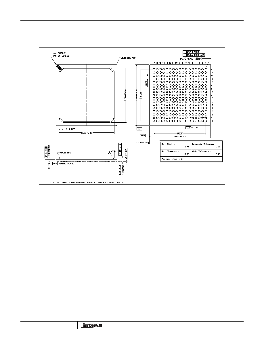
28
5 Package Dimensions
All linear dimensions in the below mechanical drawing of the BBT3420 package are in millimeters.
FIGURE 5-1. HSBGA-289 PACKAGE DIMENSIONS
BBT3420
29
6 Electrical Characteristics
6.1 Absolute Maximum Ratings
6.2 Operating Conditions
All specifications assume T
A
= 0
∞
C to +70
∞
C, V
DD
= V
DDA
= 1.8 ± 0.1V, V
DDQ
= 2.5 ± 0.2V, unless otherwise specified.
TABLE 6-1. ABSOLUTE MAXIMUM RATINGS
SYMBOL
PARAMETER
UNITS
MIN
MAX
V
DDQ
Parallel I/O Power Supply Voltage
V
-0.5
4.6
V
DDA
, V
DD
Other Power Supply Voltages
V
-0.5
2.5
V
INCML
CML DC Input Voltage
V
-0.5
V
DD
+ 0.5
V
INXSTTL
HSTL/SSTL_2 DC Input Voltage
V
-0.5
5.5
I
OUTCML
CML Output Current
mA
-50
I
OUXSTTL
HSTL/SSTL_2 Output Current
mA
50
T
STG
Storage Temperature
∞C
-65
150
T
J
Junction Temperature
∞C
-55
125
T
SOL
Soldering Temperature (10s)
∞C
220
V
ESD
Maximum Input ESD (HBM)
V
-1500
1500
These ratings are those which if exceeded may cause permanent damage to the device. Operation at these or any other conditions in excess of
those listed under Operating Conditions below is not implied. Continued exposure to these ratings may reduce device reliability.
TABLE 6-2. RECOMMENDED OPERATING CONDITIONS
SYMBOL
PARAMETER
UNITS
MIN
NOM
MAX
V
DDA
& V
DD
Core and Serial I/O Power Supply Voltages
V
1.7
1.8
1.9
V
DDQ
Parallel I/O Power Supply Voltage
V
+1.7
2.7
T
A
Ambient Operating Temperature
∞C
0
25
70
TABLE 6-3. THERMAL RESISTANCES
SYMBOL
PARAMETER
UNIT
TYP
MAX
JC
Thermal Resistance, Junction to Case
∞C/W
14
CA
Thermal Resistance, Case to Ambient
∞C/W
19
TABLE 6-4. SERIAL PIN I/O ELECTRICAL SPECIFICATIONS
SYMBOL
PARAMETER
UNITS
MIN
TYP
MAX
V
P-PIN
Peak-To-Peak Differential Voltage Input Requirement (Note 1)
mV
200
V
P-POUT
Peak-To-Peak Differential Voltage Output Amplitude
(Z
O
= 100
differential load) no Pre-emphasis
mV
1000
1300
1800
NOTE:
1. Applies for DC balanced data such as XAUI 8B/10B data. For data with long run lengths such as PRBS, DC offset compensation circuitry must
be turned off. The device default is for DC offset compensation circuitry to be turned on. See Table 3-17.
TABLE 6-5. PARALLEL PIN I/O CHARACTERISTICS, SSTL_2 (Class I, see Figure 2-1)
SYMBOL PARAMETER
UNITS
MIN
TYP
MAX
V
DDQ
Supply Voltage
V
2.3
2.5
2.7
V
REF
Reference Voltage
V
1.15
1.25
1.35
V
TT
Termination Voltage
V
V
REF
- 0.04
V
REF
V
REF
+ 0.04
V
IH(dc)
dc input logic high
V
V
REF
+ 0.18
V
DDQ
+ 0.3
BBT3420
30
V
IL(dc)
dc input logic low
V
-0.3
V
REF
- 0.18
V
IH((ac
)
ac input logic high
V
V
REF
+ 0.35
V
IL(ac)
ac input logic low
V
V
REF
- 0.35
V
OH
dc output logic high (I
OH
= 7.6mA)
V
V
DDQ
- 0.62
V
OL
dc output logic low (I
OL
= 7.6mA)
V
0.54
V
OH(ac)
ac output logic high (I
OH
= 8mA)
V
V
DDQ
- 0.5
V
OL(ac)
ac output logic low (I
OL
= 8mA)
V
0.5
TABLE 6-5. PARALLEL PIN I/O CHARACTERISTICS, SSTL_2 (Class I, see Figure 2-1)
SYMBOL PARAMETER
UNITS
MIN
TYP
MAX
TABLE 6-6. PARALLEL PIN I/O CHARACTERISTICS, HSTL (V
DDQ
= 1.8V ±0.1 V) (Class I, see Figure 2-1)
SYMBOL PARAMETER
UNITS
MIN
TYP
MAX
V
DDQ
Supply Voltage
V
1.7
1.8
1.9
V
REF
Reference Voltage
V
0.83
0.9
1.07
V
TT
Termination Voltage
V
V
DDQ
x 0.5
V
IH(dc)
dc input logic high
V
V
REF
+ 0.1
V
DDQ
+ 0.3
V
IL(dc)
dc input logic low
V
-0.3
V
REF
- 0.1
V
IH(ac)
ac input logic high
V
V
REF
+ 0.2
V
IL(ac)
ac input logic low
V
V
REF
- 0.2
V
OH(dc)
dc output logic high (I
OH
= 8 mA)
V
V
DDQ
- 0.4
V
DDQ
+ 0.3
V
OL(dc)
dc output logic low (I
OL
= 8 mA)
V
0.4
V
OH(ac)
ac output logic high (I
OH
= 8 mA)
V
V
DDQ
- 0.5
V
OL(ac)
ac output logic low (I
OL
= 8 mA)
V
0.5
TABLE 6-7. OTHER DC ELECTRICAL SPECIFICATIONS
SYMBOL
PARAMETER
UNITS
MIN
TYP
V
IH
, C
TL
Control Input High Voltage Range
V
DDQ
= 1.8
V
V
DDQ
x 0.7
V
DDQ
= 2.5V
1.7
V
IL
, C
TL
Control Input Low Voltage Range
V
DDQ
= 1.8
V
-0.3
V
DDQ
= 2.5V
V
OH
, C
TL
Status Output High Voltage Level IOH = -1mA
V
V
DDQ
- 0.4
V
OL
, C
TL
Status Output Low Voltage Level IOL = 1mA
V
0
I
IH
, C
TL
Input High Current (Magnitude), VIN = 2.4V
µ
A
I
IL
, C
TL
Input Low Current (Magnitude), VIN = 0.5V
µ
A
I
DD
+ I
DDA
Total Core Supply Current (includes high-speed
I/Os), T
A
= 25∞C
mA
600
I
DDQ-NL
I/O Supply Current, T
A
= 25∞C (no loading)
mA
TBD
I
DDQ
I/O Supply Current, T
A
= 25∞C (50
load)
mA
TBD
BBT3420
31
6-3 Timing Characteristics
All specifications assume T
A
= 0∞C to +70∞C, V
DD
= V
DDA
= 1.8 ± 0.1V, V
DDQ
= 2.5 ± 0.2V, unless otherwise specified.
TABLE 6-8. TRANSMIT PARALLEL INTERFACE TIMING (see Figure 6-1 & Figure 6-2)
SYMBOL
PARAMETER
MIN
TYP
MAX
UNIT
T
SU
Setup Time
0.4
ns
T
HOLD
Hold Time
0.4
ns
TT
LAT
(codec)
Transmitter latency with encoder enabled
65
70
UI
TT
LAT
(raw)
Transmitter latency with encoder disabled
55
65
UI
TABLE 6-9. RECEIVE PARALLEL INTERFACE TIMING (see Figure 6-3 through Figure 6-6)
SYMBOL
PARAMETER
MIN
TYP
MAX
UNIT
RT
SYNC
Bit Sync Time
2500
Bits
T
DVCC
Time data valid before the rising edge or falling edge
of the alignment clock
0.96
ns
T
CCDV
Time data valid after the rising or falling edge of the
alignment clock
0.96
ns
RT
LAT
(codec)
Receiver latency with encoder enabled
55
125
195
UI
RT
LAT
(raw)
Receiver latency with encoder disabled
45
115
185
Bits
RT
SKEWIN
Input skew between channels in trunking mode1
±3
Bytes
NOTE:
1. RT
SKEWIN
is defined as input skew to BBT3420 high speed input receiver.
TABLE 6-10. REFERENCE CLOCK REQUIREMENTS
SYMBOL
PARAMETER
MIN
TYP
MAX
UNIT
1/T
REFCLK
Ref clock frequency range (Note 1)
124.4
159.375
MHz
T
JREF
Ref clock frequency offset
-100
100
ppm
Refduty
Ref clock duty cycle
45
50
55
%
NOTE:
1. System requirements are normally much more restrictive, typically ±100ppm. This specification refers to the range over which the BBT3420 will
operate.
TABLE 6-11. TRANSMIT SERIAL DIFFERENTIAL OUTPUT TIMING (see Figure 6-12)
SYMBOL
PARAMETER
MIN
TYP
MAX
T
ODR
Rise time (20%-80%)
100
130
T
ODF
Fall time (20%-80%)
100
130
T
OCCDS
Channel to Channel Differential Skew (Note 1)
15
TX
JIT
Random Jitter (RMS, 1100 pattern) (Note 2)
2.488Gbps
2
4
3.125Gbps
2.5
4
3.1875Gbps
2.5
4
Total Jitter (RMS, encoded BIST pattern)
2.488Gbps
8
3.125Gbps (Note 3)
6
8
3.1875Gbps
8
NOTES:
1. Parameter is guaranteed by design.
2. Strictly the 1010 pattern causes a small additional non-random jitter, so that the true random jitter is slightly less than that shown.
3. Max jitter for CJPAT pattern is around 10ps.
BBT3420
32
TABLE 6-12. SERIAL DIFFERENTIAL INPUT TIMING REQUIREMENTS (see Figure 6-12)
SYMBOL
PARAMETER
MIN
TYP
MAX
UNIT
T
DJ
Deterministic Jitter (Notes 1, 2)
0.7
UI
T
JI
Total jitter tolerance
0.88
UI
NOTES:
1. Jitter specifications include all but 10
-12
of the jitter population.
2. Near end driven by BBT3420 Tx.
TABLE 6-13. RESET AND DEVAD FROM MFD, MFC TIMING (see Figure 6-9)
SYMBOL
PARAMETER
MIN
TYP
MAX
UNIT
T
RESET
RSTN Active width
10
µs
T
RSTDVS
Setup from MFD, MFC to RSTN
2
µs
T
RSTDVH
Hold from RSTN to MFD, MFC
1
T
REFCLK
T
RSTMFV
Delay from RSTN to MFD/C Valid
2
T
REFCLK
TABLE 6-14. MDIO INTERFACE TIMING (from IEEE802.3ae-2002) (see Figure 6-10)
SYMBOL
PARAMETER
MIN
TYP
MAX
UNIT
T
MDCD
BBT3420 MDIO out delay from MDC
0
300
ns
T
MDS
Setup from MDIO in to MDC
10
ns
T
RSTDVH
Hold from MDC to MDIO in
10
ns
T
RSTMFV
Clock Period MDC (Note 1)
50
400
ns
MDC Clock HI or LO time (Note 1)
20
160
ns
NOTE:
1. The BBT3420 will accept a much higher MDC clock rate and shorter HI and LO times than the IEEE802.3ae specification (section 22.2.2.11)
requires. Such a faster clock may not be acceptable to other devices on the interface.
TABLE 6-15. RESET AND BISTEN TIMING (see Figure 6-11)
SYMBOL
PARAMETER
MIN
TYP
MAX
UNIT
T
RESET
RSTN Active width
10
µs
T
RSTBIST
Delay from RSTN to BISTEN
2
T
REFCLK
T
BRST
BISTEN Inactive width
20
T
REFCLK
T
BRVD
Delay from BISTEN to valid ERR (MFA-D) Value
T
REFCLK
BBT3420

33
6.4 Timing Diagrams
FIGURE 6-1. TRANSMITTER PARALLEL TIMING
FIGURE 6-2. TRANSMITTER LATENCY
FIGURE 6-3. RECEIVER PARALLEL DATA TIMING
BBT3420
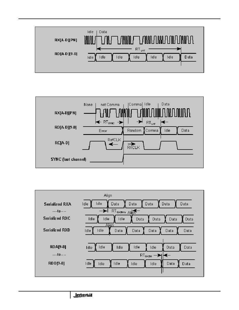
34
FIGURE 6-4. RECEIVER LATENCY
FIGURE 6-5. BYTE SYNCHRONIZATION
FIGURE 6-6. CHANNEL ALIGNMENT OPERATION
BBT3420
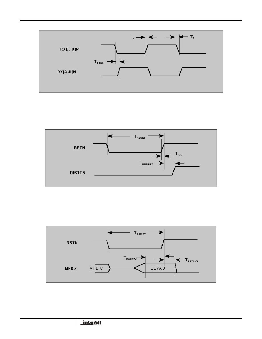
35
FIGURE 6-7. DIFFERENTIAL SIGNAL TIMING
FIGURE 6-8. RESET AND BIST ENABLE TIMING
FIGURE 6-9. SETTING DEVAD AT END OF RESET
BBT3420
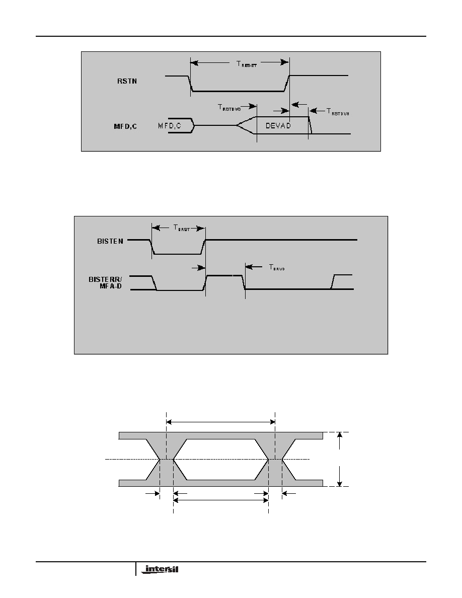
36
FIGURE 6-10. MDIO INTERFACE TIMING
FIGURE 6-11. BIST ERROR FLAG TIMING
FIGURE 6-12. EYE DIAGRAM DEFINITION AND TIMING
Vcm
Vpp (single-ended)
Total Jitter
Eye Width
Unit Interval (UI)
BBT3420
37
Applications Information
DTE XGXS (XGMII-to-XAUI) Setup
One of many applications of the BBT3420 is utilizing it as a
10Gigabit Ethernet DTE XGXS device. The following
discussion focuses on configuring the BBT3420 to operate
as a DTE XGXS device. It also assumes the default register
setting after a hard reset.
The MFC and MFD pins have internal pull-up resistors
(approx. 50k
), therefore no external resistor is needed to
configure the BBT3420 to DEVICE ADDRESS 5 (see
Table 3-5). The CODE and PSYNC pins should be pulled HI
(to V
DDQ
), and BISTEN and LPENA-D pulled LOW (to
GND); all these pins except PSYNC have internal pulls to
these values.
Some of the default register settings need to be changed, for
XGMII-to-XAUI operation. The register addresses are
described with the Clause 22 address followed by the
Clause 45 address. The default value of the A_ALIGN_DIS
bit of the Symbol and Elasticity Control MII Register
(19'h/C000'h) will cause channel alignment to occur on IDLE
to non-IDLE transitions across all four channels. This can be
changed to channel alignment on /A/ (K28.3) characters by
setting this bit to a zero, to conform to the XAUI
specification. The internal (XGMII) Error character should be
set to 1FE'h by writing FE'h to 16'h/C002'h. The pseudo-
random XAUI IDLE /A/K/R/ generator should be enabled by
setting the AKR_EN bit in register 1D'h/C001'h. To allow
complete regeneration of the Inter Packet Gap (IPG), it is
desirable to set the TRANS_EN bit in register 10'h/C001'h.
For the best XAUI-conforming performance, it is also
advisable to set the PCS_SYNC_EN and DSKW_SM_EN
bits in register 1D'h/C000'h.
All the above listed register settings can be overridden,
effectively forcing the BBT3420 to the desired conditions, by
setting the XAUI_EN bit in register 1D'h/C001'h.
Additional register settings may be desirable in certain
environments. If the incoming XAUI signals have traveled
some distance from their source (or if the source provides a
weak signal), it will usually be advisable to use the equalizer
to improve the signal integrity. Similarly, if the transmitted
XAUI signals are to travel a significant distance, pre-
emphasis may be desirable. Both these can be changed
from their default values (0'h) via register 1C'h/C005'h. It
may also be found desirable to alter the LOS detector
threshold, using register 1D'h/C001'h.
Recommended Analog Power and Ground Plane
Splits
The BBT3420 high-speed analog circuits as well as high-
speed I/O draw power from the analog power (VDDA) and
analog ground GNDA pins/balls (pins or balls will be used
inter-changeably through out this document). In order for the
BBT3420 to achieve best performance, the VDDA and
GNDA shall be kept as "quiet" as possible.
The VDDA voltage requirement of the BBT3420 is 1.8V. The
ripple noise on the VDDA voltage rail shall be as low as
possible for best jitter performance. Therefore, in the layout,
VDDA shall be decoupled from the main supply of 1.8V by
means of a cut out in the power plane. The 1.8V power to
VDDA is supplied through a ferrite bead (capable of 1A is
recommended). The cut out spacing shall be at least 20mil.
A "quiet" analog ground also enhances the jitter performance
of the BBT3420 as well. A similar cut out in the ground plane
is recommended. Analog ground (GNDA) shall be tied to
digital ground (GND) through a ferrite bead (capable of at
least 1A is recommended).
Recommended Power Supply Decoupling
For BBT3420, the decoupling for V
DDA
V
DD
and V
DDQ
must
all be handled individually.
VDDA (1.8V) provides power to the analog circuits as well as
the high speed I/Os. The analog power supply VDDA must
have impedance less than 0.4
from around 50kHz to
FIGURE 6-13. CHANNEL-TO-CHANNEL DIFFERENTIAL SKEW
t
OCCDS
TX[A:D]P/N
TX[A:D]P/N
BBT3420

38
All Intersil U.S. products are manufactured, assembled and tested utilizing ISO9000 quality systems.
Intersil Corporation's quality certifications can be viewed at www.intersil.com/design/quality
Intersil products are sold by description only. Intersil Corporation reserves the right to make changes in circuit design, software and/or specifications at any time without
notice. Accordingly, the reader is cautioned to verify that data sheets are current before placing orders. Information furnished by Intersil is believed to be accurate and
reliable. However, no responsibility is assumed by Intersil or its subsidiaries for its use; nor for any infringements of patents or other rights of third parties which may result
from its use. No license is granted by implication or otherwise under any patent or patent rights of Intersil or its subsidiaries.
For information regarding Intersil Corporation and its products, see www.intersil.com
1GHz. This can be achieved by using one 22µF (1210 case
size, CERAMIC), nine 0.1µF (0402 case size, ceramic), and
nine 0.01µF (0402 case size, ceramic) capacitors in parallel.
The 0.01µF and 0.1µF 0402 case size capacitors must be
placed right next to the VDDA balls as close as possible.
Note that the 22µF capacitor must be of 1210 case size, and
it must be ceramic for lowest ESR possible. The 0.01µF
must be of case size 0402, this offers the lowest ESL to
achieve low impedance towards the GHz range. Also, note
that the ground of these capacitors must be connected to
GNDA.
VDD (1.8V) is the power rail for the core logic circuit. For the
VDD, at least six 0.1µF (0402 case size), six 0.01µF (0402
case size) and a 10µF (tantalum) capacitor are
recommended. Place the 0.01µF and 0.1µF capacitors as
close to the VDD balls as possible.
V
DDQ
(1.8V or 2.5V) is the power rail for all the low speed
I/O drivers; at least ten 0.01µF (0402 case size), ten 0.1µF
(0402 case size) capacitors are recommended. Place the
0.01µF and 0.1µF capacitors as close to the V
DDQ
balls as
possible.
Ordering Information
PRODUCT
FREQUENCY
PACKAGE
ORDER PART
NUMBER
BBT3420
2.488-3.1875Gbps
BGA-289
BBT3420-SN
BBT3420