 | ÐлекÑÑоннÑй компоненÑ: CA1523E | СкаÑаÑÑ:  PDF PDF  ZIP ZIP |
Äîêóìåíòàöèÿ è îïèñàíèÿ www.docs.chipfind.ru
7-11
CAUTION: These devices are sensitive to electrostatic discharge; follow proper IC Handling Procedures.
407-727-9207
|
Copyright
©
Intersil Corporation 1999
CA1523
Voltage Regulator Control Circuit
for Variable Switching Regulator
Description
The CA1523 monolithic silicon integrated circuit is a variable
interval pulse regulator designed to provide the control cir-
cuitry for use in switching regulator circuits. It operates from
11V to 15V.
The regulator provides a single output drive capable of
300mA source/200mA sink. The maximum operating fre-
quency is better than 200kHz. An attractive feature of the
CA1523 is that the timing capacitor charge and discharge
current is set up externally via a single resistor. The ratio of
charge to discharge current is internally set at a maximum of
2 to 1 allowing simultaneous change in output pulse width
with increased frequency at higher load. The pulse width
variation at higher frequencies effectively compensates for
the losses in magnetics and thereby increases the power
supply efficiency at higher load end by as much as 20
percent.
Features
· Operates up to 200kHz
· Pins ESD Protected
· Remote ON/OFF
· Slow Start with Reset
· Overcurrent Sensing
· Lower Peak Currents than PWM Regulator
- Less Prone to Magnetic Saturation
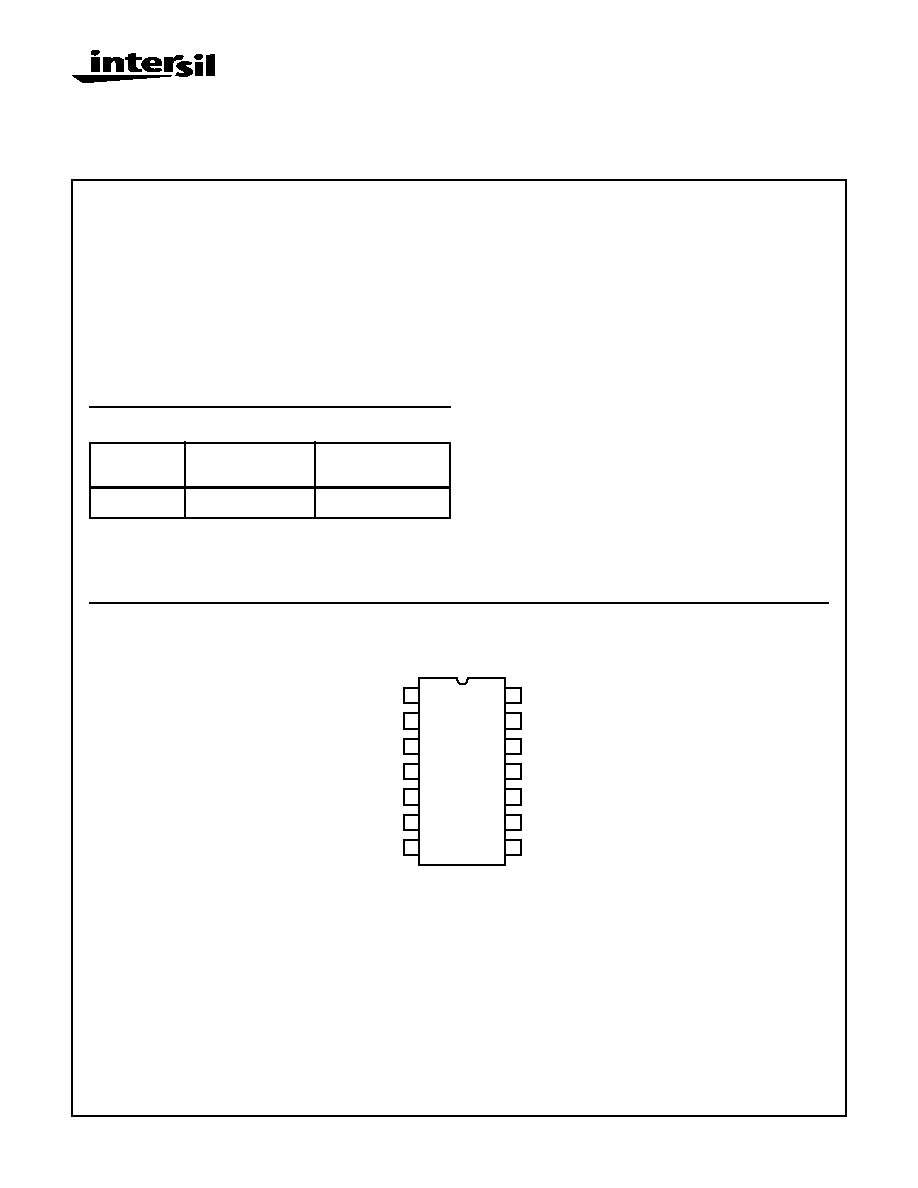
Ordering Information
PART
NUMBER
TEMPERATURE
RANGE
PACKAGE
CA1523E
0
o
C to +70
o
C
14 Lead Plastic DIP
File Number
1785.2
April 1994
Pinout
CA1523 (PDIP)
TOP VIEW
ERROR
CURRENT SENSE
GND
RISE TIME
OUTPUT GND
OUTPUT
V
CC
TIMING
ZENER
ON/OFF
OVER CURRENT
SLOW START
LOGIC OUTPUT
NC
1
2
3
4
5
6
7
14
13
12
11
10
9
8
7-12
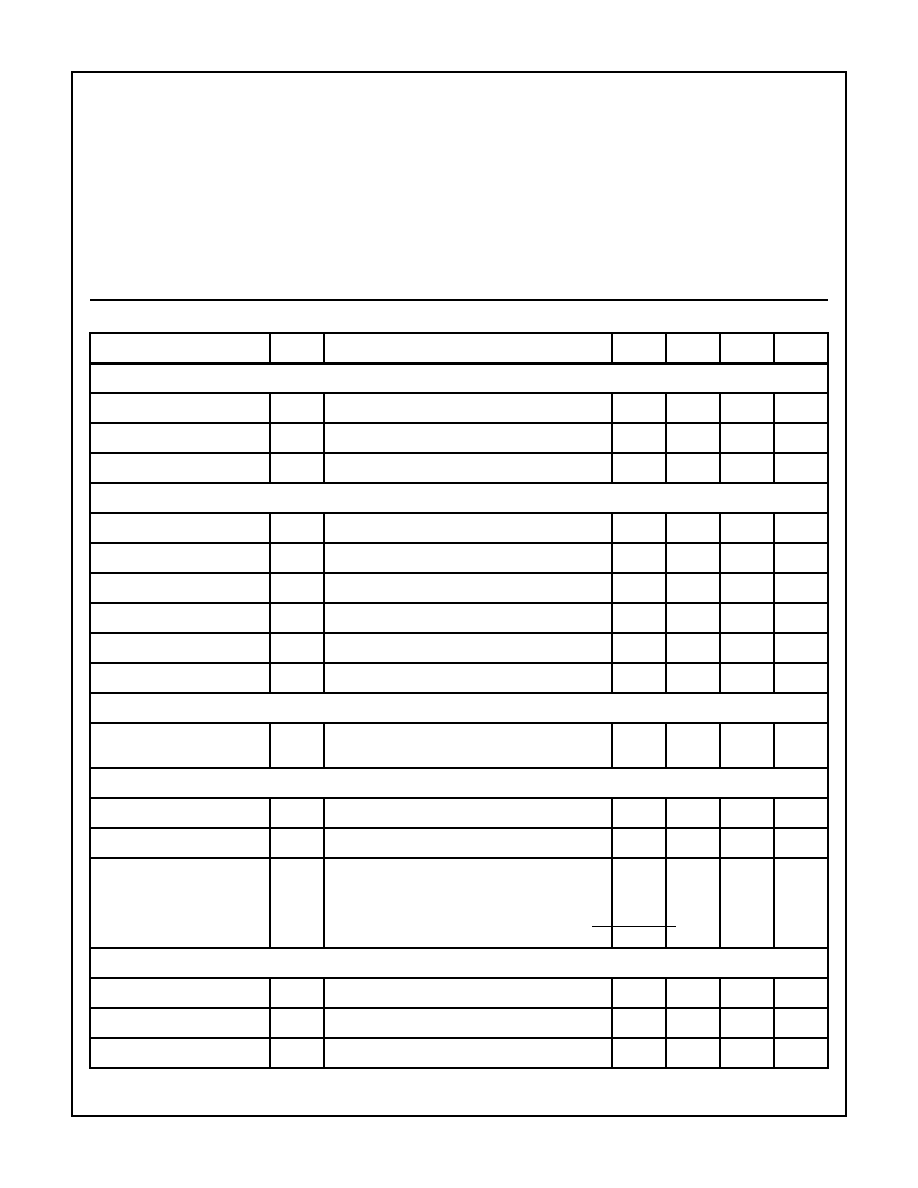
Specifications CA1523
Absolute Maximum Ratings
Thermal Information
DC Supply Voltage . . . . . . . . . . . . . . . . . . . . . . . . . . . . . . . . . . . 15V
Supply Current
|
6(MAX)
. . . . . . . . . . . . . . . . . . . . . . . . . . . . . . . . . . . . . . . . . . . . . .±
50mA
|
6(MAX)
, 1
µ
s,1800pF Load . . . . . . . . . . . . . . . . . . . . +300, -200mA
Device Dissipation
Up to T
A
= 70
o
C . . . . . . . . . . . . . . . . . . . . . . . . . . . . . . . . 530mW
Above T
A
= 70
o
C. . . . . . . . . . . . . . . Derate Linearly at 6.7mW/
o
C
Thermal Resistance
JA
Plastic DIP Package . . . . . . . . . . . . . . . . . . . . . . . .
120
o
C/W
Device Dissipation
Up to T
A
= 70
o
C. . . . . . . . . . . . . . . . . . . . . . . . . . . . . . . . . 665mW
Ambient Temperature Range
Operating. . . . . . . . . . . . . . . . . . . . . . . . . . . . . . . . . 0
o
C to +70
o
C
Storage . . . . . . . . . . . . . . . . . . . . . . . . . . . . . . . . -55
o
C to +150
o
C
Lead Temperature (During Soldering)
At distance 1/16
±
in. (1.59mm
±
0.79mm)
from case for 10s Max . . . . . . . . . . . . . . . . . . . . . . . . . . . . +265
o
C
CAUTION: Stresses above those listed in "Absolute Maximum Ratings" may cause permanent damage to the device. This is a stress only rating and operation
of the device at these or any other conditions above those indicated in the operational sections of this specification is not implied.
Electrical Specifications
T
A
= +25
o
C, Refer to condition shown in test circuit; V
7
= 13V, V
1
= 5.9V Unless Otherwise Specified
PARAMETERS
PIN
TEST CONDITIONS
MIN
TYP
MAX
UNITS
POWER SUPPLY, V
CC
(PIN 7)
Supply Voltage
7
9.5
13
-
V
Supply Current
7
V
CC
= +13V
20
27
34
mA
Zener Voltage
13
7.8
8.4
8.9
V
OUTPUT PULSE (PIN 6)
Maximum Pulse Width
6
Measured at 6V Threshold Level
5.5
6.5
7.5
µ
s
Minimum Pulse Width
6
Measured at 6V Threshold Level
2
3
4
µ
s
Output High Voltage
6
|
6
= 0mA, V
4
= 0V
11.1
12
12.6
V
Output Low Voltage
6
|
6
= 50mA, V
12
= 0V
0.6
1
1.3
V
Rise Time
6
Measured at 1.8V and 10V Threshold Levels
250
600
1250
ns
Fall Time
6
Measured at 1.8V and 10V Threshold Levels
50
200
350
ns
ERROR VOLTAGE RANGE (PIN 1)
Error Voltage Reference
1
Adjust R
T
; Observe Pin 6 Min/Max
Frequency Range
5.9
6.8
7.5
V
CHARGE CURRENT (PIN 14)
Charge Current
14
Adjust R
T
, V
1
= 7.5V; Set V
14
= 0V, Then V
14
= 2.5V
190
220
250
µ
A
Discharge Current
14
Adjust R
T
= 5.9V; Set V
14
= 5.5V, Then 5V
95
110
125
µ
A
Slow Start Discharge Current
14
Maintain V
14
= 5V, V
10
= 5.5V
Set V
10
= 5.5V, Measure I
14
(Hi)
Set V
10
= 4V, Measure I
14
(Lo)
Limits = I
14
(Hi) - I
14
(Lo)
1.5
20
30
40
µ
A/V
LOGIC TESTS
Discharge Voltage
10
Pin 12 = 1k
to GND
1.7
2.4
3.2
V
Output Inhibit Voltage
7
Increase V
7
Until V
9
2V
7.9
8.4
9.1
V
Overcurrent Trip Voltage
11
V
12
= 5V; V
10
= 0V; Increase V
11
Until V
9
0.5V
1.1
1.25
1.4
V
7-13
CA1523
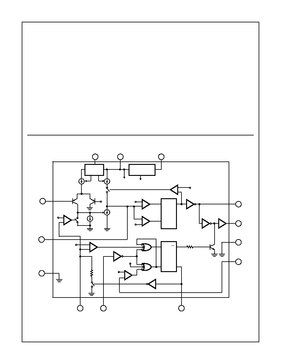
Other Desirable Features
Other desirable features along with various circuit block
function explanations are listed below.
· The Oscillator is a sawtooth generator whose charge
(rise) cycle determines the output pulse width and dis-
charge which is continuously variable from very low to
maximum of I
CHARGE
.
· Charge I
CHARGE
= I
O
-I
DISCHARGE
giving 2 to 1 pulse-width
control
· Discharge I
DISCHARGE
= approximately 0 to 1/2 I
O
to
frequency control.
· Pulse Shaping: Applied to the oscillator output via RS
Flip-Flop with parallel inhibit controlled by slow-start over-
current sense, supply voltage monitor and ON/OFF func-
tions.
· Pulse Rise Time: Modified to meet RFI requirements by
external slow-down capacitor.
· Slow Start with Reset: Externally programmed against
internal 3V reference. Reset is initiated upon Inhibit ensur-
ing soft start at power up and restart.
· Over Current Sense: Internal stable thresholds of 1.2V.
· Supply Voltage Monitors: Locks out the drive until
V
SUPPLY
has reached 8V-9V.
· ON/OFF: Activates regulator independent of raw DC.
· Error Amplifier: Compares output against a stable 6.8V
internal reference and controls the discharge current sink
on the timing capacitor.
· Band-Gap: Reference voltage (internal) provides temper-
ature compensated 1.2V and 6.8V references.
· Separate GND: The power GND is separated from circuit
ground for improved noise.
· ESD Protection: Pins are protected against ESD.
Block Diagram
14
1
7
CURRENT
SENSE
I
C/2
I
C
+6.8V
REF.
ERROR
VOLTAGE
V
CC
V
CC
10
3K
S
3
1.2V
REF.
-
+
I
D
~
I
C/2
FOR
V
I
<< 6.8V
12
ON/OFF
3
Q HIGH CLOSES S
1
S
1
CURRENT
SETUP
Q LOW
CLOSES S
3
+
-
V
CC
> 8.4V
-
+
-
+
V
L
2.5V
V
H
5V
LOGIC
OUT
9
S
R
Q
F/F
S
R
Q
F/F
4
REF. VOLTAGE
SOURCES
13
5
6
11
2
ZENER
6.8V
REF.
TIMING
CAP
GND
S
2
OPEN
WHEN V
IO
> 6.8V
3V
(CONTROL
CIRCUIT
GND)
SLOW
START
REF.
5V
REF.
RISE
TIME
PULSE
OUTPUT
OUTPUT
GND
OVER
CURRENT
I
D
7-14
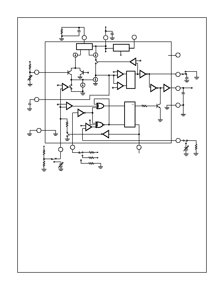
CA1523
FIGURE 1. TEST CIRCUIT FOR THE CA1523
1
14
2
-
+
-
+
3
9
12
10
+
-
11
6
5
4
7
+
8
13
V
CC
15K
20K
TRIM
RES.
R
T
ERROR
VOLTAGE
TIMING
240pF
(CONTROL
CIRCUIT
GND)
V
CC
12K
30K
V
IO
SLOW
START
ON/OFF
ON
OFF
220
220
1K
Q LOW
CLOSES
S3
S3
3K
3V
REF.
6.8V
REF
S2 OPEN
WHEN V10 > 6.8V
S2
V
CC
>6.4V
1.2V
REF.
+5V
V
CC
+6.8V
REF
I
C/2
CURRENT
SET UP
I
C
S1
Q HIGH
CLOSES S1
I
D
~
I
C/2
FOR V
I
<<6.8V
V
CC
REF. VOLT.
SOURCES
ZENER
5V
5V
NC
S
Q
R
Q
V
H
RISE/FALL
47pF
PULSE OUTPUT
1800pF
OUTPUT
GND
OVER
CURRENT
1K
V
11
LOGIC
OUT
56K
0.0033
µ
F
CHARGE
CURRENT
S
R
Q
F/F
F/F
V
CC
V
L
2.5V
+
-
REF
7-15
CA1523
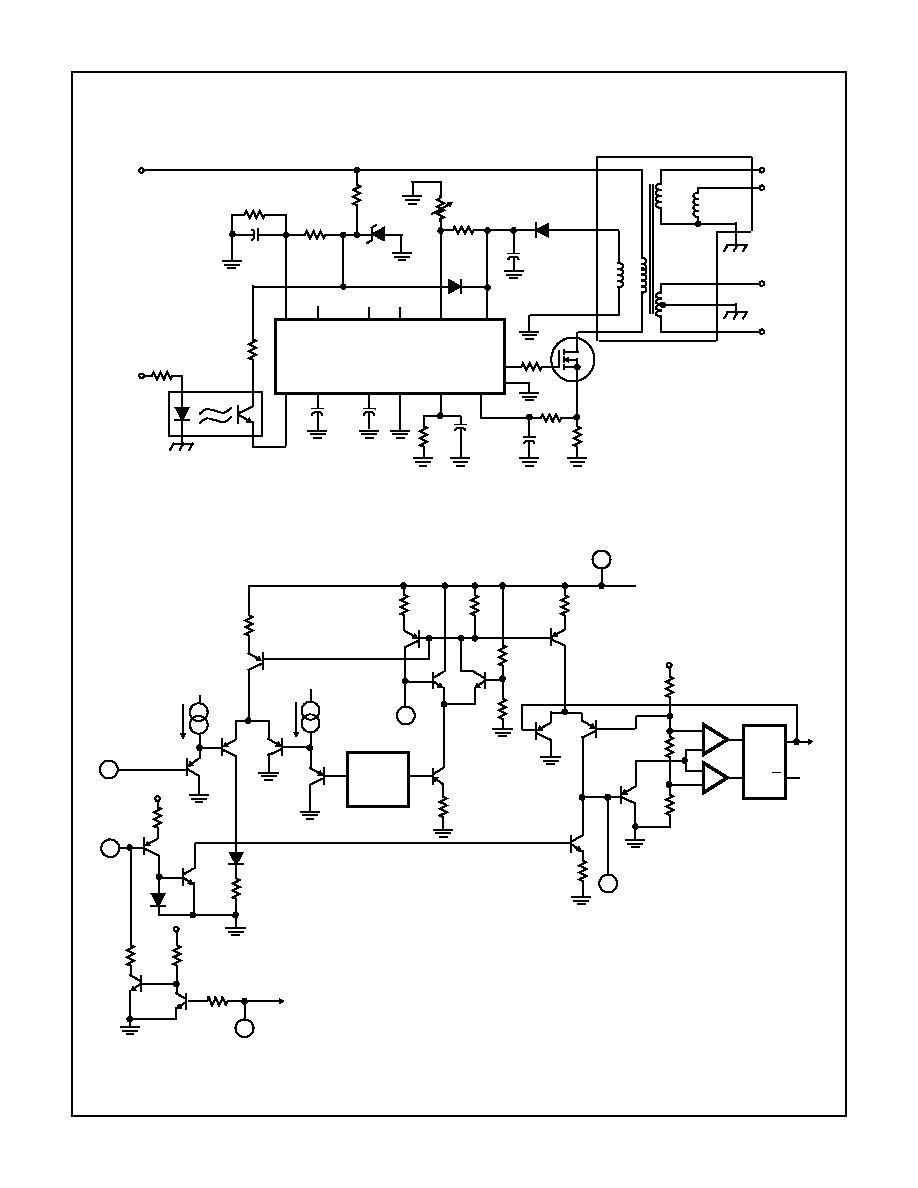
FIGURE 2. TYPICAL APPLICATION CIRCUIT FOR THE CA1523
FIGURE 3. TIMING CIRCUIT FOR THE CA1523
+150V
RECTIFIED AC LINE
INPUT
30k
1.5k
OPTO-COUPLER
11k
68
µ
F
220
68
240
68k
0.0033
22pF
0.15
3W
10k
47
NC
NC
NC
RFP 7N40
11V
20k (TRIM RESISTOR)
5.6k
10W
4.7
µ
F
SENSE
FEEDBACK
PRIMAR
Y
SEC. "D"
SEC. "C"
SEC. "D"
SEC. "A"
TRANSFORMER
TYP. INPUT
+150
0.85A
------------
16k
13V
+
12
4
14
3
2
11
5
6
7
1
13
9
8
10
CA1523
pF
pF
µ
F
+
ON/OFF
BIAS
VOLT-
AGE
V
04
V
02
V
01
V
03
TYPICAL
RECT.
OUTPUT
+130V
-24V
+16V
+24V
9
10
1
+
+
2
7
14
LOGIC OUT
6K
3K
12K
SLOW
START
+V
CC
30K
1.5K
ERROR
+7.5V
8.3K
6.8V
1.21V
1.8K
BAND
GAP
REF
VOLTAGE
8K
15K
4K
10K
10K
V
CC
1.5K
2K
2K
2.5V
5.0V
+
-
+
-
V
L
V
H
R
S
Q
Q
+7.5V
2K
+V
CC