1
Semiconductor
CAUTION: These devices are sensitive to electrostatic discharge; follow proper IC Handling Procedures.
Copyright
©
Harris Corporation 1999
CA3028A
Differential/Cascode Amplifier for
Commercial and Industrial Equipment
from DC to 120MHz
The CA3028A is a differential/cascode amplifier designed for
use in communications and industrial equipment operating
at frequencies from DC to 120MHz.
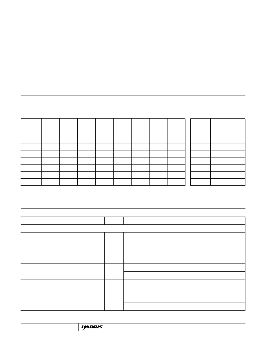
Pinouts
CA3028A
(PDIP, SOIC)
TOP VIEW
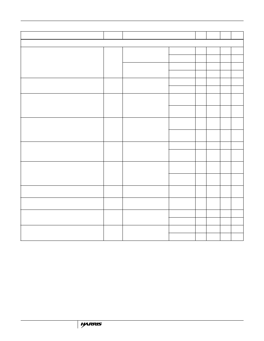
CA3028A
(METAL CAN)
TOP VIEW
Features
∑ Controlled for Input Offset Voltage, Input Offset
Current and Input Bias Current
∑ Balanced Differential Amplifier Configuration with Con-
trolled Constant Current Source
∑ Single-Ended and Dual-Ended Operation
Applications
∑ RF and IF Amplifiers (Differential or Cascode)
∑ DC, Audio and Sense Amplifiers
∑ Converter in the Commercial FM Band
∑ Oscillator
∑ Mixer
∑ Limiter
∑ Related Literature
- Application Note AN5337 "Application of the CA3028
Integrated Circuit Amplifier in the HF and VHF Ranges."
This note covers characteristics of different operating
modes, noise performance, mixer, limiter, and amplifier
design considerations
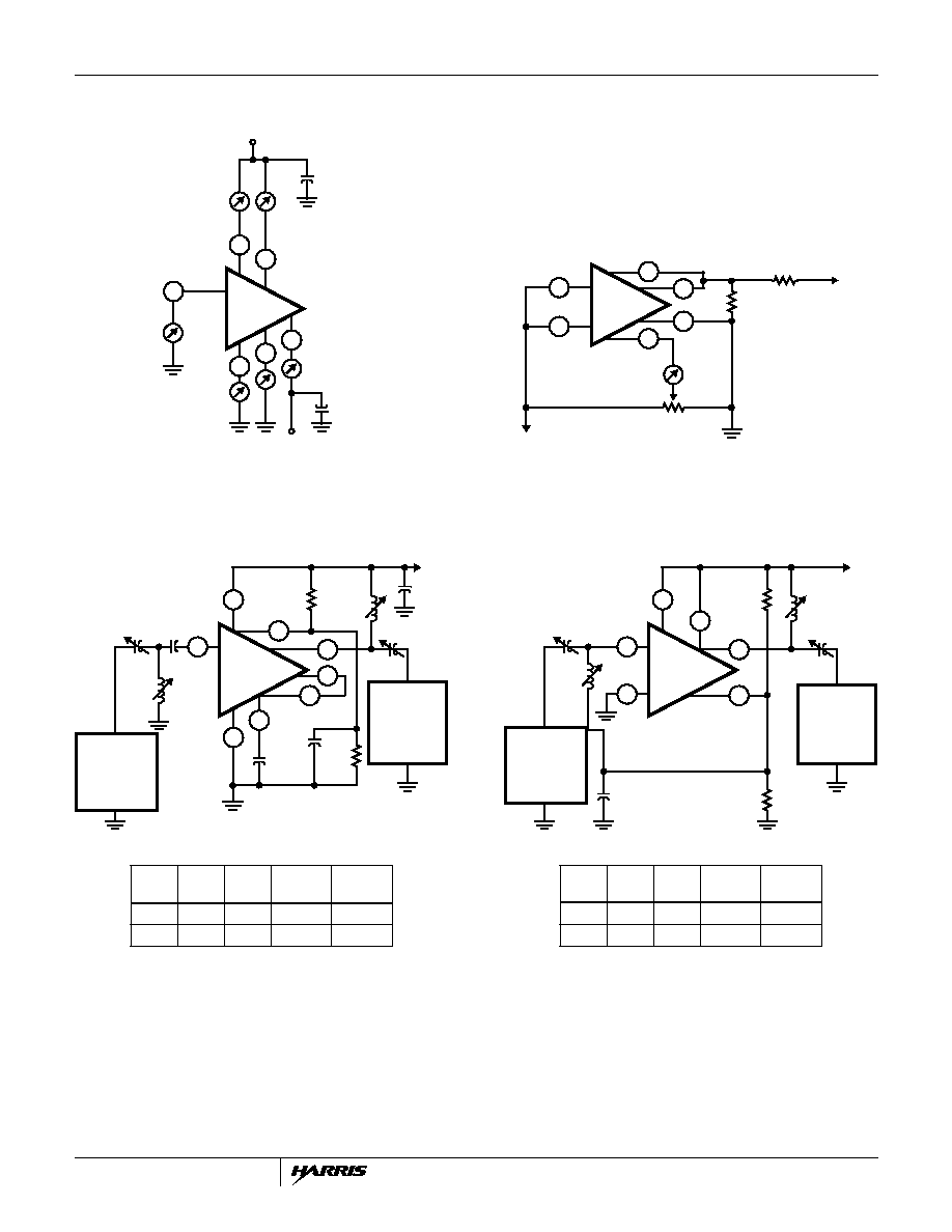
Schematic Diagram
(Terminal Numbers Apply to All Packages)
Part Number Information
PART NUMBER
(BRAND)
TEMP.
RANGE (
o
C)
PACKAGE
PKG.
NO.
CA3028A
-55 to 125
8 Pin Metal Can
T8.C
CA3028AE
-55 to 125
8 Ld PDIP
E8.3
CA3028AM96
(3028A)
-55 to 125
8 Ld SOIC Tape
and Reel
M8.15
1
2
3
4
8
7
6
5
2
4
6
1
3
7
5
8
3
4
5
8
6
1
7
2
R
2
2.8k
R
3
500
SUBSTRATE
R
1
5k
Q
1
Q
2
Q
3
AND CASE
January 1999
File Number
382.5
[ /Title
(CA30
28A)
/Sub-
ject
(Dif-
feren-
tial/Ca
scode
Ampli-
fier for
Com-
mer-
cial
and
Indus-
trial
Equip-
ment
from
DC to
120M
Hz)
/Autho
r ()
/Key-
words
(Har-
ris
Semi-
OBSOLETE PR
ODUCT
NO RECOMMENDED REPLA
CEMENT
Call Central Applications 1-800-442-7747
or email: centapp@harris.com
2
Operating Conditions
Thermal Information
Temperature Range . . . . . . . . . . . . . . . . . . . . . . . . . -55
o
C to 125
o
C
Thermal Resistance (Typical, Note 1)
JA
(
o
C/W)
JC
(
o
C/W)
Metal Can Package . . . . . . . . . . . . . . .
225
140
PDIP Package . . . . . . . . . . . . . . . . . . .
155
N/A
SOIC Package . . . . . . . . . . . . . . . . . . .
185
N/A
Maximum Junction Temperature (Metal Can Package). . . . . . . .175
o
C
Maximum Junction Temperature (Plastic Package) . . . . . . . .150
o
C
Maximum Storage Temperature Range . . . . . . . . . . -65
o
C to 150
o
C
Maximum Lead Temperature (Soldering 10s) . . . . . . . . . . . . 300
o
C
(SOIC - Lead Tips Only)
CAUTION: Stresses above those listed in "Absolute Maximum Ratings" may cause permanent damage to the device. This is a stress only rating and operation of the
device at these or any other conditions above those indicated in the operational sections of this specification is not implied.
NOTE:
1.
JA
is measured with the component mounted on an evaluation PC board in free air.
Absolute Maximum Voltage Ratings
T
A
= 25
o
C
Absolute Maximum
Current Ratings
The following chart gives the range of voltages which can be applied to the terminals listed horizontally with
respect to the terminals listed vertically. For example, the voltage range of the horizontal Terminal 4 with
respect to Terminal 2 is -1V to +5V.
TERM
NO.
1
2
3
4
5
6
7
8
TERM
NO.
I
IN
mA
I
OUT
mA
1
0 to -15
0 to -15
0 to -15
+5 to -5
Note 3
Note 3
+20 to 0
1
0.6
0.1
2
+5 to -11
+5 to -1
+15 to 0
Note 3
+15 to 0
Note 3
2
4
0.1
3 (Note 2)
+10 to 0
+15 to 0
+24 to 0
+15 to 0
+24 to 0
3
0.1
23
4
+15 to 0
Note 3
Note 3
Note 3
4
20
0.1
5
+20 to 0
Note 3
Note 3
5
0.6
0.1
6
Note 3
Note 3
6
20
0.1
7
Note 3
7
4
0.1
8
8
20
0.1
NOTES:
2. Terminal No. 3 is connected to the substrate and case.
3. Voltages are not normally applied between these terminals. Voltages appearing between these terminals
will be safe, if the specified voltage limits between all other terminals are not exceeded.
Electrical Specifications
T
A
= 25
o
C
PARAMETER
SYMBOL
TEST CONDITIONS
MIN
TYP
MAX
UNIT
DC CHARACTERISTICS
Input Bias Current (Figures 1, 10)
I
I
V
CC
= 6V, V
EE
= -6V
-
16.6
70
µ
A
V
CC
= 12V, V
EE
= -12V
-
36
106
µ
A
Quiescent Operating Current (Figures 1,11, 12)
I
6
, I
8
V
CC
= 6V, V
EE
= -6V
0.8
1.25
2.0
mA
V
CC
= 12V, V
EE
= -12V
2.0
3.3
5.0
mA
AGC Bias Current (Into Constant Current Source
Terminal 7) (Figures 2, 13)
I
7
V
CC
= 12V, V
AGC
= 9V
-
1.28
-
mA
V
CC
= 12V, V
AGC
= 12V
-
1.65
-
mA
Input Current (Terminal 7)
I
7
V
CC
= 6V, V
EE
= -6V
0.5
0.85
1.0
mA
V
CC
= 12V, V
EE
= -12V
1.0
1.65
2.1
mA
Power Dissipation (Figures 1, 14)
P
T
V
CC
= 6V, V
EE
= -6V
24
36
54
mW
V
CC
= 12V, V
EE
= -12V
120
175
260
mW
CA3028A
3
DYNAMIC CHARACTERISTICS
Power Gain (Figures 3, 4, 5, 15, 17, 19)
G
P
f = 100MHz
V
CC
= 9V
Cascode
16
20
-
dB
Diff. Amp.
14
17
-
dB
f = 10.7MHz
V
CC
= 9V
Cascode
35
39
-
dB
Diff. Amp.
28
32
-
dB
Noise Figure (Figures 3, 4, 5, 16, 18, 19)
NF
f = 100MHz, V
CC
= 9V
Cascode
-
7.2
9.0
dB
Diff. Amp.
-
6.7
9.0
dB
Input Admittance (Figures 20, 21)
Y
11
f = 10.7MHz, V
CC
= 9V
Cascode
-
0.6 +
j1.6
-
mS
Diff. Amp.
-
0.5 +
j0.5
-
mS
Reverse Transfer Admittance (Figures 22, 23)
Y
12
f = 10.7MHz, V
CC
= 9V
Cascode
-
0.0003
- j0
-
mS
Diff. Amp.
-
0.01 -
j0.0002
-
mS
Forward Transfer Admittance (Figures 24, 25)
Y
21
f = 10.7MHz, V
CC
= 9V
Cascode
-
99 - j18
-
mS
Diff. Amp.
-
-37 +
j0.5
-
mS
Output Admittance (Figures 26, 27)
Y
22
f = 10.7MHz, V
CC
= 9V
Cascode
-
0 +
j0.08
-
mS
Diff. Amp.
-
0.04 +
j0.23
-
mS
Output Power (Untuned) (Figures 6, 28)
P
O
f = 10.7MHz, V
CC
= 9V
Diff. Amp., 50
Input-Output
-
5.7
-
µ
W
AGC Range (Maximum Power Gain to Full Cutoff)
(Figures 7, 29)
AGC
f = 10.7MHz, V
CC
= 9V
Diff. Amp.
-
62
-
dB
Voltage Gain
(Figures 8, 9, 30, 31)
A
f = 10.7MHz, V
CC
= 9V,
R
L
= 1k
Cascode
-
40
-
dB
Diff. Amp.
-
30
-
dB
Peak-to-Peak Output Current
I
P-P
f = 10.7MHz, e
IN
= 400mV,
Diff. Amp.
V
CC
= 9V
2.0
4.0
7.0
mA
V
CC
= 12V
3.5
6.0
10
mA
Electrical Specifications
T
A
= 25
o
C (Continued)
PARAMETER
SYMBOL
TEST CONDITIONS
MIN
TYP
MAX
UNIT
CA3028A
4
Test Circuits
NOTE:
.
FIGURE 1. INPUT OFFSET CURRENT, INPUT BIAS CURRENT,
POWER DISSIPATION, AND QUIESCENT
OPERATING CURRENT TEST CIRCUIT
FIGURE 2. AGC BIAS CURRENT TEST CIRCUIT (DIFFERENTIAL
AMPLIFIER CONFIGURATION)
NOTES:
4. For Power Gain Test.
5. For Noise Figure Test.
FIGURE 3. POWER GAIN AND NOISE FIGURE TEST CIRCUIT
(CASCODE CONFIGURATION)
NOTES:
6. For Power Gain Test.
7. For Noise Figure Test.
FIGURE 4. POWER GAIN AND NOISE FIGURE TEST CIRCUIT
(DIFFERENTIAL AMPLIFIER CONFIGURATION
AND TERMINAL 7 CONNECTED TO V
CC
)
Power Dissipation
I
3
V
EE
I
6
I
8
+
(
)
V
CC
+
=
ICUT
5
7
3
6
8
3
µ
F
1
3
µ
F
V
CC
V
EE
I
1
-
+
-
+
-
+
I
6
I
8
-
+
I
5
I
7
I
3
-
+
-
+
ICUT
3
5
1
6
I
7
8
V
CC
1k
2k
7
5k
V
CC
ICUT
8
5
6
2
1
3
4
0.001
µ
F
50
SIGNAL
SOURCE
(NOTE 4) OR
NOISE DIODE
50
RF
VOLTMETER
(NOTE 4) OR
NOISE AMP
(NOTE 5)
C
2
C
1
470pF
L
1
(NOTE 5)
0.001
µ
F
2k
7
V
CC
L
2
1k
0.001
µ
F
f
(MHz)
C
1
(pF)
C
2
(pF)
L
1
(
µ
H)
L
2
(
µ
H)
10.7
20 - 60 20 - 60
3 - 5
3 - 5
100
3 - 30
3 - 30
0.1 - 0.25 0.15 - 0.3
ICUT
6
1
5
50
SIGNAL
SOURCE
(NOTE 6) OR
NOISE DIODE
50
RF
VOLTMETER
(NOTE 6) OR
NOISE AMP
(NOTE 7)
C
2
C
1
L
1
(NOTE 7)
0.001
µ
F
2k
8
V
CC
L
2
1k
f
(MHz)
C
1
(pF)
C
2
(pF)
L
1
(
µ
H)
L
2
(
µ
H)
10.7
30 - 60 20 - 50
3 - 6
3 - 6
100
2 - 15
2 - 15
0.2 - 0.5
0.2 - 0.5
3
7
CA3028A

5
NOTES:
8. For Power Gain Test.
9. For Noise Figure Test.
FIGURE 5. POWER GAIN AND NOISE FIGURE TEST CIRCUIT
(DIFFERENTIAL AMPLIFIER CONFIGURATION)
FIGURE 6. OUTPUT POWER TEST CIRCUIT
FIGURE 7. AGC RANGE TEST CIRCUIT (DIFFERENTIAL
AMPLIFIER)
FIGURE 8. TRANSFER CHARACTERISTIC (VOLTAGE GAIN) TEST
CIRCUIT (10.7MHz) CASCODE CONFIGURATION
Test Circuits
(Continued)
ICUT
6
1
5
50
SIGNAL
SOURCE
(NOTE 8) OR
NOISE DIODE
50
RF
VOLTMETER
(NOTE 8) OR
NOISE AMP
(NOTE 9)
C
2
C
1
L
1
(NOTE 9)
0.001
µ
F
2k
7
V
CC
L
2
1k
f
(MHz)
C
1
(pF)
C
2
(pF)
L
1
(
µ
H)
L
2
(
µ
H)
10.7
30 - 60 20 - 50
3 - 6
3 - 6
100
2 - 15
2 - 15
0.2 - 0.5
0.2 - 0.5
3
8
5k
ICUT
6
7
8
5
1
3
0.01
50
0.01
µ
F
OUTPUT
V
CC
50
2k
INPUT
1k
0.01
µ
F
V
CC
0.01
µ
F
µ
F
ICUT
6
1
5
C
2
C
1
L
1
2k
7
V
CC
L
2
1k
f
(MHz)
C
1
(pF)
C
2
(pF)
L
1
(
µ
H)
L
2
(
µ
H)
10.7
30 - 60 20 - 50
3 - 6
3 - 6
100
2 - 15
2 - 15
0.2 - 0.5
0.2 - 0.5
3
8
5k
50
RF
VOLTMETER
50
SIGNAL
SOURCE
0.001
µ
F
ICUT
6
1
8
3
7
0.01
µ
F
2
INPUT
0.01
µ
F
50
4
5
0.01
µ
F
2k
0.01
µ
F
1k
LOAD
10
OUTPUT
1k
V
CC
CA3028A