 | –≠–ª–µ–∫—Ç—Ä–æ–Ω–Ω—ã–π –∫–æ–º–ø–æ–Ω–µ–Ω—Ç: CA3060 | –°–∫–∞—á–∞—Ç—å:  PDF PDF  ZIP ZIP |
3-1
Semiconductor
January 1999
CA3060
110kHz, Operational
Transconductance Amplifier Array
CAUTION: These devices are sensitive to electrostatic discharge. Users should follow proper IC Handling Procedures.
Copyright
©
Harris Corporation 1999
File Number
537.4
Features
∑ Low Power Consumption as Low as 100mW Per
Amplifier
∑ Independent Biasing for Each Amplifier
∑ High Forward Transconductance
∑ Programmable Range of Input Characteristics
∑ Low Input Bias and Input Offset Current
∑ High Input and Output Impedance
∑ No Effect on Device Under Output Short-Circuit
Conditions
∑ Zener Diode Bias Regulator
Applications
∑ For Low Power Conventional Operational Amplifier
Applications
∑ Active Filters
∑ Comparators
∑ Gyrators
∑ Mixers
∑ Modulators
∑ Multiplexers
∑ Multipliers
∑ Strobing and Gating Functions
∑ Sample and Hold Functions
Description
The CA3060 monolithic integrated circuit consists of an array of
three independent Operational Transconductance Amplifiers
(see Note). This type of amplifier has the generic characteris-
tics of an operational voltage amplifier with the exception that
the forward gain characteristic is best described by transcon-
ductance rather than voltage gain (open-loop voltage gain is the
product of the transconductance and the load resistance,
g
M
R
L
). When operated into a suitable load resistor and with
provisions for feedback, these amplifiers are well suited for a
wide variety of operational-amplifier and related applications. In
addition, the extremely high output impedance makes these
types particularly well suited for service in active filters.
The three amplifiers in the CA3060 are identical push-pull
Class A types which can be independently biased to achieve a
wide range of characteristics for specific application. The elec-
trical characteristics of each amplifier are a function of the
amplifier bias current (I
ABC
). This feature offers the system
designer maximum flexibility with regard to output current capa-
bility, power consumption, slew rate, input resistance, input bias
current, and input offset current. The linear variation of the
parameters with respect to bias and the ability to maintain a
constant DC level between input and output of each amplifier
also makes the CA3060 suitable for a variety of nonlinear appli-
cations such as mixers, multipliers, and modulators.
In addition, the CA3060 incorporates a unique Zener diode
regulator system that permits current regulation below sup-
ply voltages normally associated with such systems.
NOTE: Generic applications of the OTA are described in AN-6668.
For improved input operating ranges, refer to CA3080 and CA3280
data sheets (File Nos. 475 and 1174) and application notes AN6668
and AN6818.
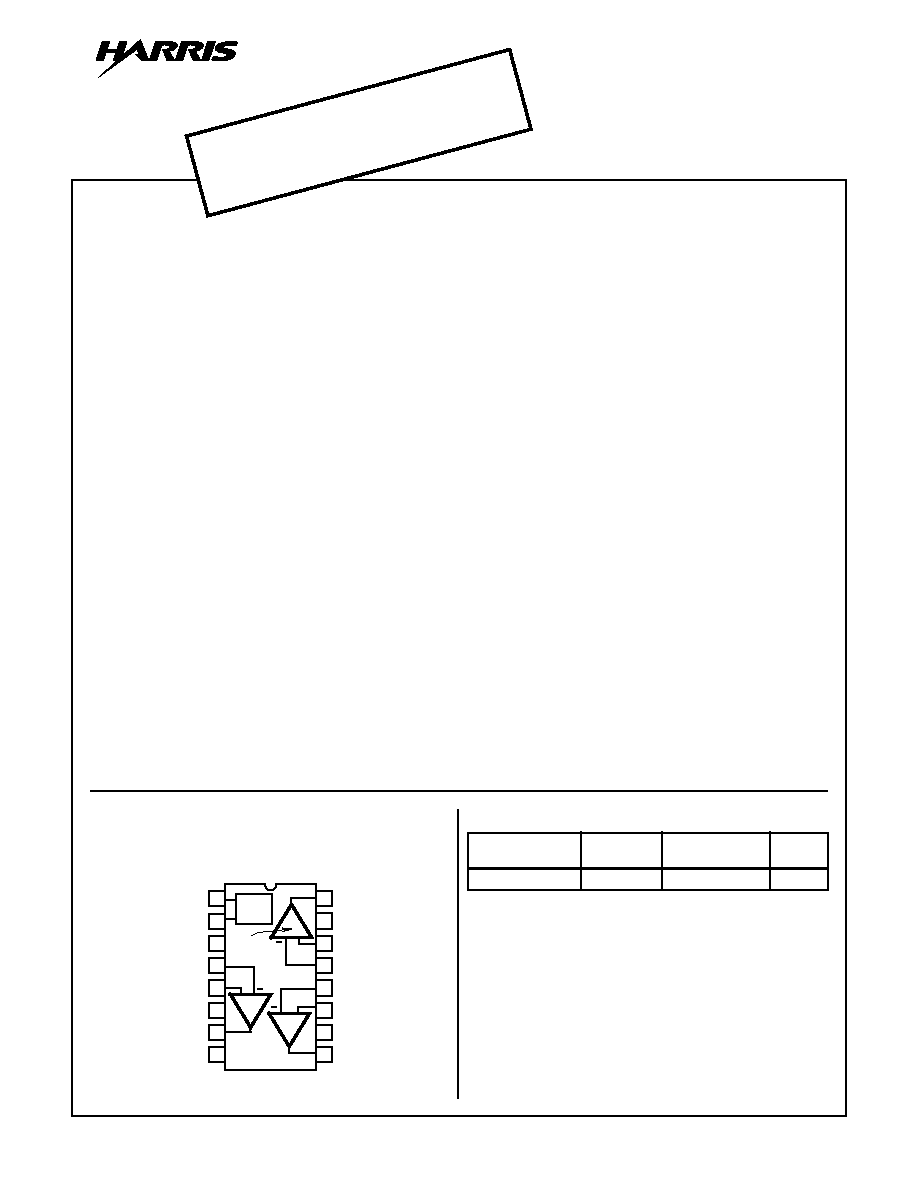
Pinout
CA3060
(PDIP)
TOP VIEW
14
15
16
9
13
12
11
10
1
2
3
4
5
7
6
8
+
+
+
AMP 1
BIAS
REG.
REGULATOR OUT
REGULATOR IN
V+
INV. INPUT NO. 3
NON-INV. INPUT NO. 3
BIAS NO. 3
OUTPUT NO. 3
V-
OUTPUT NO. 1
BIAS NO. 1
NON-INV. INPUT NO. 1
INV. INPUT NO. 1
INV. INPUT NO. 2
NON-INV. INPUT NO. 2
BIAS NO. 2
OUTPUT NO. 2
AMP
3
AMP
2
Part Number Information
PART NUMBER
TEMP.
RANGE (
o
C)
PACKAGE
PKG.
NO.
CA3060E
-40 to 85
16 Ld PDIP
E16.3
[ /Title
(CA30
60)
/Sub-
ject
(110k
Hz,
Opera-
tional
Transc
onduc-
tance
Ampli-
fier
Array)
/Autho
r ()
/Key-
words
(Har-
ris
Semi-
con-
ductor,
triple,
transco
nduc-
tance
ampli-
fier,
low
power
op
amp,
OBSOLETE PR
ODUCT
NO RECOMMENDED REPLA
CEMENT
Call Central Applications 1-800-442-7747
or email: centapp@harris.com

3-2
Absolute Maximum Ratings
Operating Conditions
Supply Voltage (Between V+ and V- Terminals) . . . . . . . 36V (
±
18V)
Input Voltage. . . . . . . . . . . . . . . . . . . . . . . . . . . . . . . . . . . . . V+ to V-
Differential Input Voltage (Each Amplifier) . . . . . . . . . . . . . . . . . . 5V
Input Current (Each Amplifier)
. . . . . . . . . . . . . . . . . . . . . . . . . . . . ±
1mA
Amplifier Bias Current (Each Amplifier) . . . . . . . . . . . . . . . . . . . 2mA
Bias Regulator Input Current . . . . . . . . . . . . . . . . . . . . . . . . . . -5mA
Output Short Circuit Duration (Note 1) . . . . . . . . . . . . . . . . Indefinite
Temperature Range . . . . . . . . . . . . . . . . . . . . . . . . . -40
o
C to 85
o
C
Thermal Information
Thermal Resistance (Typical, Note 2)
JA
(
o
C/W)
PDIP Package . . . . . . . . . . . . . . . . . . . . . . . . . . . . .
90
Maximum Junction Temperature (Plastic Package) . . . . . . . 150
o
C
Maximum Storage Temperature Range . . . . . . . . . -65
o
C to 150
o
C
Maximum Lead Temperature (Soldering 10s) . . . . . . . . . . . . 300
o
C
CAUTION: Stresses above those listed in "Absolute Maximum Ratings" may cause permanent damage to the device. This is a stress only rating and operation
of the device at these or any other conditions above those indicated in the operational sections of this specification is not implied.
NOTES:
1. Short circuit may be applied to ground or to either supply.
2.
JA
is measured with the component mounted on an evaluation PC board in free air.
Electrical Specifications
T
A
= 25
o
C, V
SUPPLY
=
±
15V
PARAMETER
SYMBOL
AMPLIFIER BIAS CURRENT
UNITS
I
ABC
= 1
µ
A
I
ABC
= 10
µ
A
I
ABC
= 100
µ
A
MIN
TYP
MAX
MIN
TYP
MAX
MIN
TYP
MAX
Input Offset Voltage
(See Figure 1)
V
IO
-
1
-
-
1
-
-
1
5
mV
Input Offset Current
(See Figure 2)
I
IO
-
3
-
-
30
-
-
250
1000
nA
Input Bias Current
(See Figures 3, 4)
I
IB
-
33
-
-
300
-
-
2500
5000
nA
Peak Output Current
(See Figures 5, 6)
I
OM
-
2.3
-
-
26
-
150
240
-
µ
A
Peak Output Voltage
(See Figure 7)
Positive
V
OM
+
-
13.6
-
-
13.6
-
12
13.6
-
V
Negative
V
OM
-
-
14.7
-
-
14.7
-
12
14.7
-
V
Amplifier Supply Current (Each
Amplifier)
(See Figures 8, 9)
I
A
-
8.5
-
-
85
-
-
850
1200
µ
A
Power Consumption
(Each Amplifier)
P
-
0.26
-
-
2.6
-
-
26
36
mW
Input Offset Voltage Sensitivity
(Note 3)
Positive
V
IO
/
V+
-
1.5
-
-
2
-
-
2
150
µ
V/V
Negative
V
IO
/
V-
-
20
-
-
20
-
-
30
150
µ
V/V
Amplifier Bias Voltage
(Note 4, See Figure 10)
V
ABC
-
0.54
-
-
0.60
-
-
0.66
-
V
DYNAMIC CHARACTERISTICS At 1kHz, Unless Otherwise Specified
Forward Transconductance
(Large Signal)
(See Figures 11, 12)
g
21
-
1.55
-
-
18
-
30
102
-
mS
Common Mode Rejection
Ratio
CMRR
-
110
-
-
110
-
70
90
-
dB
Common Mode Input Voltage
Range
V
ICR
+12 to
-12
+13 to
-14
-
+12 to
-12
+13 to
-14
-
+12 to
-12
+13 to
-14
-
V
Slew Rate (Test Circuit)
(See Figure 17)
SR
-
0.1
-
-
1
-
-
8
-
V/
µ
s
Open Loop (g
21
) Bandwidth
(See Figure 13)
BW
OL
-
20
-
-
45
-
-
110
-
kHz
CA3060

3-3
Input Impedance Components
Resistance (See Figure 14)
R
I
-
1600
-
-
170
-
10
20
-
k
Capacitance at 1MHz
C
I
-
2.7
-
-
2.7
-
-
2.7
-
pF
Output Impedance Components
Resistance (See Figure 15)
R
O
-
200
-
-
20
-
-
2
-
M
Capacitance at 1MHz
C
O
-
4.5
-
-
4.5
-
-
4.5
-
pF
ZENER BIAS REGULATOR CHARACTERISTICS I
2
= 0.1mA
Voltage (See Figure 16)
V
Z
Temperature
Coefficient = 3mV/
o
C
6.2
6.7
7.9
V
Impedance
Z
Z
-
200
300
NOTES:
3. Conditions for Input Offset Voltage Sensitivity:
a. Bias current derived from the regulator with an appropriate resistor connected from Terminal 1 to the bias terminal on the amplifier
under test V+ is reduced to +13V for V+ sensitivity and V- is reduced to -13V for V- sensitivity.
b. V+ Sensitivity in
,
V- Sensitivity in
.
4. Temperature Coefficient; -2.2mV/
o
C (at V
ABC
= 0.54, I
ABC
= 1
µ
A); -2.1mV/
o
C (at V
ABC
= 0.060V, I
ABC
= 10
µ
A); -1.9mV/
o
C (at V
ABC
= 0.66V,
I
ABC
= 100
µ
A)
Electrical Specifications
T
A
= 25
o
C, V
SUPPLY
=
±
15V (Continued)
PARAMETER
SYMBOL
AMPLIFIER BIAS CURRENT
UNITS
I
ABC
= 1
µ
A
I
ABC
= 10
µ
A
I
ABC
= 100
µ
A
MIN
TYP
MAX
MIN
TYP
MAX
MIN
TYP
MAX
µ
V V
/
V
O ffset
V
O ffset
for +13V and -15V Supplies
≠
1V
------------------------------------------------------------------------------------------------------------------------------
=
µ
V V
/
V
O ffset
V
O ffset
for -13V and +15V Supplies
≠
1V
------------------------------------------------------------------------------------------------------------------------------
=
Schematic Diagram
BIAS REGULATOR AND ONE OPERATIONAL TRANSCONDUCTANCE AMPLIFIER
NOTES:
5. Inverting Input of Amplifiers 1, 2 and 3 is on Terminals 13, 12 and 4, respectively.
6. Non-inverting Input of Amplifiers 1, 2 and 3 is Terminals 14, 11 and 5, respectively.
7. Amplifier Bias Current of Amplifiers 1, 2 and 3 is on Terminals 15, 10 and 6, respectively.
8. Output of Amplifiers 1, 2 and 3 is on Terminals 16, 9 and 7, respectively.
2
1
D
4
D
5
Q
10
INVERTING INPUT
Q
1
Q
2
D
1
-
+
I
ABC
(NOTE 5)
NON-INVERTING INPUT
(NOTE 6)
ZENER BIAS REGULATOR
AMPLIFIER BIAS INPUT
(NOTE 7)
Q
3
Q
6
Q
7
D
2
Q
5
3
8
D
3
Q
8
OUTPUT (NOTE 8)
V+
V-
Q
4
CA3060

3-4
Typical Performance Curves
FIGURE 1. INPUT OFFSET VOLTAGE vs AMPLIFIER BIAS
CURRENT
FIGURE 2. INPUT OFFSET CURRENT vs AMPLIFIER BIAS
CURRENT
FIGURE 3. INPUT BIAS CURRENT vs AMPLIFIER BIAS CURRENT
FIGURE 4. INPUT BIAS CURRENT vs TEMPERATURE
FIGURE 5. PEAK OUTPUT CURRENT vs AMPLIFIER BIAS
CURRENT
FIGURE 6. PEAK OUTPUT CURRENT vs TEMPERATURE
1
10
100
1000
2.0
1.5
1.0
0.5
0.0
AMPLIFIER BIAS CURRENT (
µ
A)
INPUT OFFSET V
O
L
T
A
GE (mV)
125
o
C
25
o
C
-55
o
C
SUPPLY VOLTAGE:
V
S
=
±
15
V
S
=
±
6
AMPLIFIER BIAS CURRENT (
µ
A)
1
10
100
1000
1000
100
10
1
INPUT OFFSET CURRENT (nA)
SUPPLY VOLTAGE:
V
S
=
±
15
V
S
=
±
6
T
A
= 25
o
C
MAXIMUM
TYPICAL
1
10
100
1000
AMPLIFIER BIAS CURRENT (
µ
A)
10
1
0.1
0.01
TYPICAL
MAXIMUM
INPUT BIAS CURRENT (
µ
A)
T
A
= 25
o
C
SUPPLY VOLTAGE:
V
S
=
±
15
V
S
=
±
6
SUPPLY VOLTAGE: V
S
=
±
6
V
S
=
±
15
I
ABC
= 100
µ
A
I
ABC
= 10
µ
A
I
ABC
= 1
µ
A
-75
-50
-25
0
25
50
75
100
125
TEMPERATURE (
o
C)
10
1.0
0.1
0.01
INPUT BIAS CURRENT (
µ
A)
PEAK OUTPUT CURRENT (
µ
A)
TYPICAL
MINIMUM
AMPLIFIER BIAS CURRENT (
µ
A)
1
10
100
1000
1000
100
10
1
T
A
= 25
o
C
SUPPLY VOLTAGE:
V
S
=
±
15
V
S
=
±
6
1000
100
10
1
PEAK OUTPUT CURRENT (
µ
A)
-75
-50
-25
0
25
50
75
100
125
TEMPERATURE (
o
C)
I
ABC
= 100
µ
A
I
ABC
= 30
µ
A
I
ABC
= 10
µ
A
I
ABC
= 3
µ
A
I
ABC
= 1
µ
A
SUPPLY VOLTAGE: V
S
=
±
6
V
S
=
±
15
CA3060

3-5
FIGURE 7. PEAK OUTPUT VOLTAGE vs AMPLIFIER BIAS
CURRENT
FIGURE 8. AMPLIFIER SUPPLY CURRENT (EACH AMPLIFIER)
vs AMPLIFIER BIAS CURRENT
FIGURE 9. AMPLIFIER SUPPLY CURRENT (EACH AMPLIFIER)
vs TEMPERATURE
FIGURE 10. AMPLIFIER BIAS VOLTAGE vs AMPLIFIER BIAS
CURRENT
FIGURE 11. FORWARD TRANSCONDUCTANCE vs AMPLIFIER
BIAS CURRENT
FIGURE 12. FORWARD TRANSCONDUCTANCE vs
TEMPERATURE
Typical Performance Curves
(Continued)
1
10
100
1000
14
13
12
6
5
4
3
-3
-4
-5
-6
-12
-13
-14
-15
AMPLIFIER BIAS CURRENT (
µ
A)
PEAK OUTPUT V
O
L
T
A
GE (V)
V
OM
+ (TYP)
±
15V SUPPLY
V
OM
+ (MIN)
±
15V SUPPLY
V
OM
+ (TYP)
±
6V SUPPLY
V
OM
+ (MIN)
±
6V SUPPLY
V
OM
- (MIN)
±
6V SUPPLY
V
OM
- (TYP)
±
6V SUPPLY
V
OM
- (MIN)
±
15V SUPPLY
V
OM
- (TYP)
±
15V SUPPLY
1
10
100
1000
10,000
1000
100
10
AMPLIFIER BIAS CURRENT (
µ
A)
AMPLIFIER SUPPL
Y CURRENT (
µ
A)
MAXIMUM
TYPICAL
T
A
= 25
o
C
SUPPLY VOLTAGE:
V
S
=
±
15
V
S
=
±
6
I
ABC
= 100
µ
A
I
ABC
= 30
µ
A
I
ABC
= 10
µ
A
I
ABC
= 3
µ
A
I
ABC
= 1
µ
A
1000
100
10
1
-75
-50
-25
0
25
50
75
100
125
TEMPERATURE (
o
C)
AMPLIFIER SUPPL
Y CURRENT (
µ
A)
SUPPLY VOLTAGE: V+ = 6V, V- = -6V
V+ = 15V, V- = -15V
800
750
700
650
600
550
500
AMPLIFIER BIAS V
O
L
T
A
GE (mV)
AMPLIFIER BIAS CURRENT (
µ
A)
1
10
100
1000
SUPPLY VOLTAGE: VV
S
=
±
6
V
S
=
±
15
T
A
= 25
o
C, f = 1kHz
SUPPLY VOLTAGE: V
S
=
±
6
V
S
=
±
15
TYPICAL
MINIMUM
1000
100
10
1
1
10
100
1000
FOR
W
ARD TRANSCONDUCT
ANCE (mS)
AMPLIFIER BIAS CURRENT (
µ
A)
1000
100
10
1
-50
-25
0
25
50
75
100
125
TEMPERATURE (
o
C)
FOR
W
ARD TRANSCONDUCT
ANCE (S)
I
ABC
= 100
µ
A
I
ABC
= 30
µ
A
I
ABC
= 10
µ
A
I
ABC
= 1
µ
A
T
A
= 25
o
C, f = 1kHz
SUPPLY VOLTAGE:
V
S
=
±
15
V
S
=
±
6
CA3060