 | –≠–ª–µ–∫—Ç—Ä–æ–Ω–Ω—ã–π –∫–æ–º–ø–æ–Ω–µ–Ω—Ç: CA3094 | –°–∫–∞—á–∞—Ç—å:  PDF PDF  ZIP ZIP |
3-12
CA3094, CA3094A, CA3094B
30MHz, High Output Current Operational
Transconductance Amplifier (OTA)
The CA3094 is a differential input power control
switch/amplifier with auxiliary circuit features for ease of
programmability. For example, an error or unbalance signal
can be amplified by the CA3094 to provide an on-off signal or
proportional control output signal up to 100mA. This signal is
sufficient to directly drive high current thyristors, relays, DC
loads, or power transistors. The CA3094 has the generic
characteristics of the CA3080 operational amplifier directly
coupled to an integral Darlington power transistor capable of
sinking or driving currents up to 100mA.
The gain of the differential input stage is proportional to the
amplifier bias current (I
ABC
), permitting programmable
variation of the integrated circuit sensitivity with either digital
and/or analog programming signals. For example, at an I
ABC
of 100
µ
A, a 1mV change at the input will change the output
from 0 to 100
µ
A (typical).
The CA3094 is intended for operation up to 24V and is
especially useful for timing circuits, in automotive equipment,
and in other applications where operation up to 24V is a
primary design requirement (see Figures 28, 29 and 30 in
Typical Applications text). The CA3094A and CA3094B are
like the CA3094 but are intended for operation up to 36V and
44V, respectively (single or dual supply).
Features
∑ CA3094E, M for Operation Up to 24V
∑ CA3094AT, E, M for Operation Up to 36V
∑ CA3094BT, M for Operation Up to 44V
∑ Designed for Single or Dual Power Supply
∑ Programmable: Strobing, Gating, Squelching, AGC
Capabilities
∑ Can Deliver 3W (Average) or 10W (Peak) to External Load
(in Switching Mode)
∑ High Power, Single Ended Class A Amplifier will Deliver
Power Output of 0.6W (1.6W Device Dissipation)
∑ Total Harmonic Distortion (THD) at 0.6W in Class A
Operation 1.4% (Typ)
Applications
∑ Error Signal Detector: Temperature Control with
Thermistor Sensor; Speed Control for Shunt Wound DC
Motor
∑ Over Current, Over Voltage, Over Temperature Protectors
∑ Dual Tracking Power Supply with CA3085
∑ Wide Frequency Range Oscillator
∑ Analog Timer
∑ Level Detector
∑ Alarm Systems
∑ Voltage Follower
∑ Ramp Voltage Generator
∑ High Power Comparator
∑ Ground Fault Interrupter (GFI) Circuits
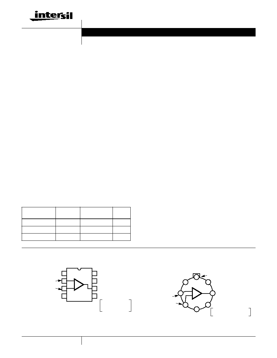
Pinouts
Ordering Information
PART NUMBER
(BRAND)
TEMP.
RANGE (
o
C)
PACKAGE
PKG.
NO.
CA3094AT, BT
-55 to 125
8 Pin Metal Can
T8.C
CA3094E, AE
-55 to 125
8 Ld PDIP
E8.3
CA3094M, BM
-55 to 125
8 Ld SOIC
M8.15
CA3094 (PDIP, SOIC)
TOP VIEW
CA3094 (METAL CAN)
TOP VIEW
NOTE: Pin 4 is connected to case.
EXT. FREQUENCY
GND (V- IN DUAL
1
2
3
4
8
7
6
5
SINK OUTPUT
V+
DRIVE OUTPUT
I
ABC
CURRENT
COMPENSATION
OR INHIBIT INPUT
SUPPLY OPERATION)
(COLLECTOR)
(EMITTER)
PROGRAMMABLE
(STROBE OR AGC)
DIFFERENTIAL
VOLTAGE INPUTS
INPUT
SINK OUTPUT
DRIVE OUTPUT
GND (V- IN DUAL
EXT. FREQUENCY
V+
2
4
6
1
3
7
5
8
DIFFERENTIAL
VOLTAGE INPUTS
COMPENSATION OR
INHIBIT INPUT
(COLLECTOR)
(EMITTER)
I
ABC
CURRENT
PROGRAMMABLE INPUT
(STROBE OR AGC)
SUPPLY OPERATION)
TAB
Data Sheet
April 1999
File Number
598.7
CAUTION: These devices are sensitive to electrostatic discharge; follow proper IC Handling Procedures.
1-888-INTERSIL or 321-724-7143
|
Copyright
©
Intersil Corporation 1999
3-13
Absolute Maximum Ratings
Thermal Information
Supply Voltage (Between V+ and V- Terminals)
CA3094 . . . . . . . . . . . . . . . . . . . . . . . . . . . . . . . . . . . . . . . . . 24V
CA3094A . . . . . . . . . . . . . . . . . . . . . . . . . . . . . . . . . . . . . . . . 36V
CA3094B . . . . . . . . . . . . . . . . . . . . . . . . . . . . . . . . . . . . . . . . 44V
Differential Input Voltage (Terminals 2 and 3, Note 1) . . . . . . . . . 5V
DC Input Voltage . . . . . . . . . . . . . . . . . . . . . . . . . . . . . . . . . V+ to V-
Input Current (Terminals 2 and 3) . . . . . . . . . . . . . . . . . . . . . .
±
1mA
Amplifier Bias Current (Terminal 5) . . . . . . . . . . . . . . . . . . . . . . 2mA
Average Output Current . . . . . . . . . . . . . . . . . . . . . . . . . . . . . 100mA
Peak Output Current . . . . . . . . . . . . . . . . . . . . . . . . . . . . . . . 300mA
Operating Conditions
Temperature Range . . . . . . . . . . . . . . . . . . . . . . . . . -55
o
C to 125
o
C
Thermal Resistance (Typical, Note 2)
JA
(
o
C/W)
JC
(
o
C/W)
PDIP Package . . . . . . . . . . . . . . . . . . .
130
N/A
SOIC Package . . . . . . . . . . . . . . . . . . .
170
N/A
Metal Can Package . . . . . . . . . . . . . . .
175
100
Maximum Junction Temperature (Metal Can Package) . . . . . . .175
o
C
Maximum Junction Temperature (Plastic Package) . . . . . . . .150
o
C
Maximum Storage Temperature Range . . . . . . . . . . -65
o
C to 150
o
C
Maximum Lead Temperature (Soldering 10s) . . . . . . . . . . . . 300
o
C
(SOIC - Lead Tips Only)
CAUTION: Stresses above those listed in "Absolute Maximum Ratings" may cause permanent damage to the device. This is a stress only rating and operation of the
device at these or any other conditions above those indicated in the operational sections of this specification is not implied.
NOTES:
1. Exceeding this voltage rating will not damage the device unless the peak input signal current (1mA) is also exceeded.
2.
JA
is measured with the component mounted on an evaluation PC board in free air.
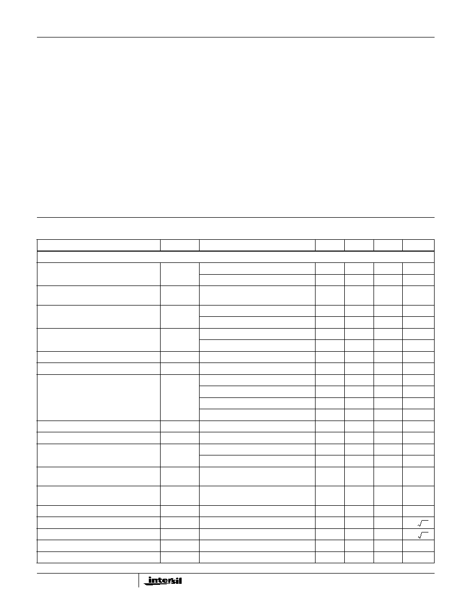
Electrical Specifications
T
A
= 25
o
C for Equipment Design. Single Supply V+ = 30V, Dual Supply V
SUPPLY
=
±
15V, I
ABC
= 100
µ
A Unless
Otherwise Specified
PARAMETER
SYMBOL
TEST CONDITIONS
MIN
TYP
MAX
UNITS
INPUT PARAMETERS
Input Offset Voltage
V
IO
T
A
= 25
o
C
-
0.4
5.0
mV
T
A
= 0
o
C to 70
o
C
-
-
7.0
mV
Input Offset Voltage Change
|
V
IO
|
Change in V
IO
between I
ABC
= 100
µ
A
and I
ABC
= 5
µ
A
-
1
8.0
mV
Input Offset Current
I
IO
T
A
= 25
o
C
-
0.02
0.2
µ
A
T
A
= 0
o
C to 70
o
C
-
-
0.3
µ
A
Input Bias Current
I
I
T
A
= 25
o
C
-
0.2
0.50
µ
A
T
A
= 0
o
C to 70
o
C
-
-
0.70
µ
A
Device Dissipation
P
D
I
OUT
= 0mA
8
10
12
mW
Common Mode Rejection Ratio
CMRR
70
110
-
dB
Common Mode Input Voltage Range
V
ICR
V+ = 30V (High)
27
28.8
-
V
V- = 0V (Low)
1.0
0.5
-
V
V+ = 15V
12
13.8
-
V
V- = -15V
-14
-14.5
-
V
Unity Gain Bandwidth
f
T
I
C
= 7.5mA, V
CE
= 15V, I
ABC
= 500
µ
A
-
30
-
MHz
Open Loop Bandwidth at -3dB Point
BW
OL
I
C
= 7.5mA, V
CE
= 15V, I
ABC
= 500
µ
A
-
4
-
kHz
Total Harmonic Distortion
(Class A Operation)
THD
P
D
= 220mW
-
0.4
-
%
P
D
= 600mW
-
1.4
-
%
Amplifier Bias Voltage
(Terminal 5 to Terminal 4)
V
ABC
-
0.68
-
V
Input Offset Voltage Temperature
Coefficient
V
IO
/
T
-
4
-
µ
V/
o
C
Power Supply Rejection
V
IO
/
V
-
15
150
µ
V/V
1/F Noise Voltage
E
N
f = 10Hz, I
ABC
= 50
µ
A
-
18
-
1/F Noise Current
I
N
f = 10Hz, I
ABC
= 50
µ
A
-
1.8
-
Differential Input Resistance
R
I
I
ABC
= 20
µ
A
0.50
1.0
-
M
Differential Input Capacitance
C
I
f = 1MHz, V+ = 30V
-
2.6
-
pF
nV/
Hz
pA/
Hz
CA3094, CA3094A, CA3094B
3-14
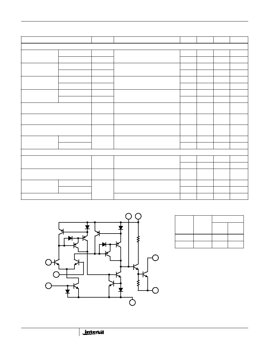
OUTPUT PARAMETERS (Differential Input Voltage = 1V)
Peak Output Voltage
(Terminal 6)
With Q
13
"ON"
V
OM
+
V+ = 30V, R
L
= 2k
to GND
26
27
-
V
With Q
13
"OFF"
V
OM
-
-
0.01
0.05
V
Peak Output Voltage
(Terminal 6)
Positive
V
OM
+
V+ = 15V, V- = -15V, R
L
= 2k
to -15V
11
12
-
V
Negative
V
OM
-
-
-14.99
-14.95
V
Peak Output Voltage
(Terminal 8)
With Q
13
"OFF"
V
OM
+
V+ = 30V, R
L
= 2k
to 30V
29.95
29.99
-
V
With Q
13
"ON"
V
OM
-
-
0.040
-
V
Peak Output Voltage
(Terminal 8)
Positive
V
OM
+
V+ = 15V, V- = -15V,
R
L
= 2k
to 15V
14.95
14.99
-
V
Negative
V
OM
-
-
-14.96
-
V
Collector-to-Emitter Saturation Voltage
(Terminal 8)
V
CE(
SAT
)
V+ = 30V, I
C
= 50mA, Terminal 6
Grounded
-
0.17
0.80
V
Output Leakage Current
(Terminal 6 to Terminal 4)
V+ = 30V
-
2
10
µ
A
Composite Small Signal Current Transfer
Ratio (Beta) (Q
12
and Q
13
)
hFE
V+ = 30V, V
CE
= 5V, I
C
= 50mA
16,000
100,000
-
Output Capacitance
Terminal 6
C
O
f = 1MHz, All Remaining Terminals Tied
to Terminal 4
-
5.5
-
pF
Terminal 8
-
17
-
pF
TRANSFER PARAMETERS
Voltage Gain
A
V+ = 30V, I
ABC
= 100
µ
A,
V
OUT
= 20V,
R
L
= 2k
20,000
100,000
-
V/V
86
100
-
dB
Forward Transconductance to
Terminal 1
gM
1650
2200
2750
µ
S
Slew Rate (Open
Loop)
Positive Slope
SR
I
ABC
= 500
µ
A, R
L
= 2k
-
500
-
V/
µ
s
Negative Slope
-
50
-
V/
µ
s
Unity Gain (Non-Inverting Compensated)
I
ABC
= 500
µ
A, R
L
= 2k
-
0.70
-
V/
µ
s
Electrical Specifications
T
A
= 25
o
C for Equipment Design. Single Supply V+ = 30V, Dual Supply V
SUPPLY
=
±
15V, I
ABC
= 100
µ
A Unless
Otherwise Specified (Continued)
PARAMETER
SYMBOL
TEST CONDITIONS
MIN
TYP
MAX
UNITS
Schematic Diagram
6
"SINK"
OUTPUT
"SOURCE"
(DRIVE)
Q
13
Q
12
R
1
2k
OUTPUT
R
2
47k
Q
10
Q
11
Q
8
Q
9
D
4
Q
7
Q
6
D
3
2
3
Q
4
D
2
Q
5
Q
2
Q
1
5
Q
3
D
6
D
5
DIFFERENTIAL
VOLTAGE
V+
EXTERNAL FREQUENCY
COMPENSATION OR INHIBIT INPUT
INPUT
AMPLIFIER
BIAS INPUT
I
ABC
D
1
DIFFERENTIAL
VOLTAGE
INPUT
V-
4
7
1
8
OUTPUT
MODE
OUTPUT
TERM
INPUTS
INV
NON-
INV
"Source"
6
2
3
"Sink"
8
3
2
CA3094, CA3094A, CA3094B
3-15
Operating Considerations
The "Sink" Output (Terminal 8) and the "Drive" Output
(Terminal 6) of the CA3094 are not inherently current (or
power) limited. Therefore, if a load is connected between
Terminal 6 and Terminal 4 (V- or Ground), it is important to
connect a current limiting resistor between Terminal 8 and
Terminal 7 (V+) to protect transistor Q13 under shorted load
conditions. Similarly, if a load is connected between Terminal
8 and Terminal 7 (V+), the current limiting resistor should be
connected between Terminal 6 and Terminal 4 or ground. In
circuit applications where the emitter of the output transistor
is not connected to the most negative potential in the
system, it is recommended that a 100
current limiting
resistor be inserted between Terminal 7 and the V+ supply.
1/F Noise Measurement Circuit
When using the CA3094, A, or B audio amplifier circuits, it is
frequently necessary to consider the noise performance of the
device. Noise measurements are made in the circuit shown in
Figure 20. This circuit is a 30dB, non-inverting amplifier with
emitter follower output and phase compensation from
Terminal 2 to ground. Source resistors (R
S
) are set to 0
or
1M
for E noise and I noise measurements, respectively.
These measurements are made at frequencies of 10Hz,
100Hz and 1kHz with a 1Hz measurement bandwidth. Typical
values for 1/f noise at 10Hz and 50
µ
A I
ABC
are:
and
.
E
N
18nV
Hz
/
=
I
N
1.8pA
Hz
/
=
Test Circuits
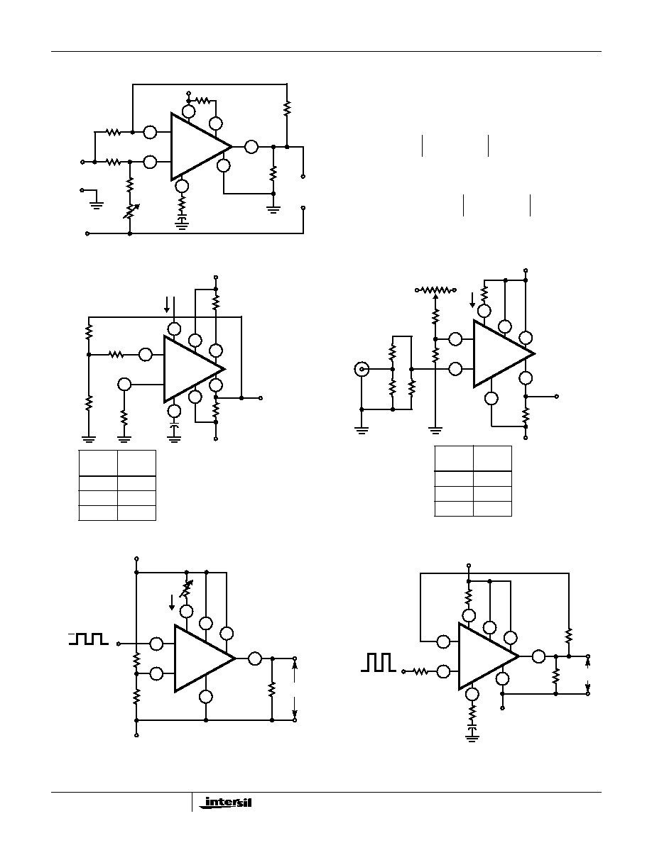
FIGURE 1. INPUT OFFSET VOLTAGE AND POWER SUPPLY REJECTION TEST CIRCUIT
FIGURE 2. INPUT OFFSET CURRENT TEST CIRCUIT
FIGURE 3. INPUT BIAS CURRENT TEST CIRCUIT
CA3094
2
3
1
4
8
6
5
7
E
OUT
30V
15V
100
100
1k
100pF
10k
9.9k
300k
30V
NOTES:
3. Input Offset Voltage:
.
4. For Power Supply Rejection Test: (1) vary V+ by -2V; then (2)
vary V- by +2V.
5. Equations:
6. Power Supply Rejection:
.
Maximum Reading of Step 1 or Step 2
V
IO
E
OUT
100
-----------------
=
V+ Rejection
E
0
OUT
E
1
OUT
≠
200
-------------------------------------------------
=
V- Rejection
E
0
OUT
E
2
OUT
≠
200
-------------------------------------------------
=
(1)
(2)
dB
(
)
20
1
V
REJECTION
---------------------------------------------
log
=
CA3094
2
1
4
6
8
7
E
OUT
15V
1M
220
0.001
µ
F
150k
1M
30V
3
5
R
ABC
NOTES:
7. P
DISSIPATION
= (V+)(I)
8. I
OS
E
OUT
106
VOLTS
AMPS
---------------------
--------------------------------
=
CA3094A
2
3
4
5
7
300k
30V
-
+
NOTE: I
I
I
2
---
=
15V
CA3094, CA3094A, CA3094B
3-16
FIGURE 4. COMMON MODE RANGE AND REJECTION RATIO TEST CIRCUIT
FIGURE 5. 1/F NOISE TEST CIRCUIT
FIGURE 6. OPEN LOOP GAIN vs FREQUENCY TEST CIRCUIT
FIGURE 7. OPEN LOOP SLEW RATE vs I
ABC
TEST CIRCUIT
FIGURE 8. SLEW RATE vs NON-INVERTING UNITY GAIN
TEST CIRCUIT
Test Circuits
(Continued)
NOTES:
9.
.
10. Input Voltage Range for CMRR = 1V to 27V.
11.
.
CMRR
100
26V
◊
E
2OUT
E
1OUT
≠
--------------------------------------------
=
CMRR (dB)
20
100
26V
◊
E
2OUT
E
1OUT
≠
--------------------------------------------
log
=
CA3094
2
3
4
1
6
8
7
E
OUT
9.9k
1k
100pF
10k
10k
4.7k
30V
-
+
200
100
100
15V
V
CMR
0.8V TO 27.2V
CA3094A
2
6
1
4
8
5
-15V
120
3k
C
C
500
7
I
ABC
3.6k
R
S
R
S
-
+
+15V
OUTPUT
(RMS)
I
ABC
(
µ
A)
C
COMP
(pF)
5
0
50
50
500
500
NOTE:
R
S
= 1M
(1/F Noise Current Test).
R
S
= 0
(1/F Noise Voltage Test).
(NOTE)
(NOTE)
3
CA3094A
2
3
6
4
8
5
-15V
R
L
= 2k
7
I
ABC
10k
-
+
+15V
OUTPUT
10
91
100
10
10k
+15V
-15V
R
S
R
S
(
)
I
ABC
(
µ
A)
56K
500
560K
50
56M
5
CA3094A
2
3
6
4
8
5
2k
7
I
ABC
-
+
13k
-15V
15k
+15V
2V
0V
E
OUT
CA3094A
2
3
6
4
8
5
2k
7
-
+
-15V
10k
+15V
±
10V
1
E
OUT
220
0.001
µ
F
10k
56k
CA3094, CA3094A, CA3094B