1
TM
File Number
1345.5
CAUTION: These devices are sensitive to electrostatic discharge; follow proper IC Handling Procedures.
1-888-INTERSIL or 321-724-7143
|
Intersil and Design is a trademark of Intersil Corporation.
|
Copyright
©
Intersil Corporation 2000
CA3227
High-Frequency NPN Transistor Array For
Low-Power Applications at Frequencies
Up to 1.5GHz
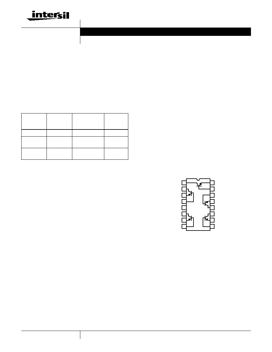
The CA3227 consists of five general purpose silicon NPN
transistors on a common monolithic substrate. Each of the
transistors exhibits a value of f
T
in excess of 3GHz, making
them useful from DC to 1.5GHz. The monolithic construction
of these devices provides close electrical and thermal
matching of the five transistors.
Features
∑ Gain-Bandwidth Product (f
T
) . . . . . . . . . . . . . . . . . >3GHz
∑ Five Transistors on a Common Substrate
Applications
∑ VHF Amplifiers
∑ VHF Mixers
∑ Multifunction Combinations - RF/Mixer/Oscillator
∑ IF Converter
∑ IF Amplifiers
∑ Sense Amplifiers
∑ Synthesizers
∑ Synchronous Detectors
∑ Cascade Amplifiers
Pinout
CA3227
(PDIP, SOIC)
TOP VIEW
Ordering Information
PART
NUMBER
(BRAND)
TEMP.
RANGE (
o
C)
PACKAGE
PKG. NO.
CA3227E
-55 to 125
16 Ld PDIP
E16.3
CA3227M
(3227)
-55 to 125
16 Ld SOIC
M16.15
CA3227M96
(3227)
-55 to 125
16 Ld SOIC Tape
and Reel
M16.15
14
15
16
9
13
12
11
10
1
2
3
4
5
7
6
8
SUBSTRATE
Q
4
Q
3
Q
2
Q
5
Q
1
Data Sheet
May 2000
2
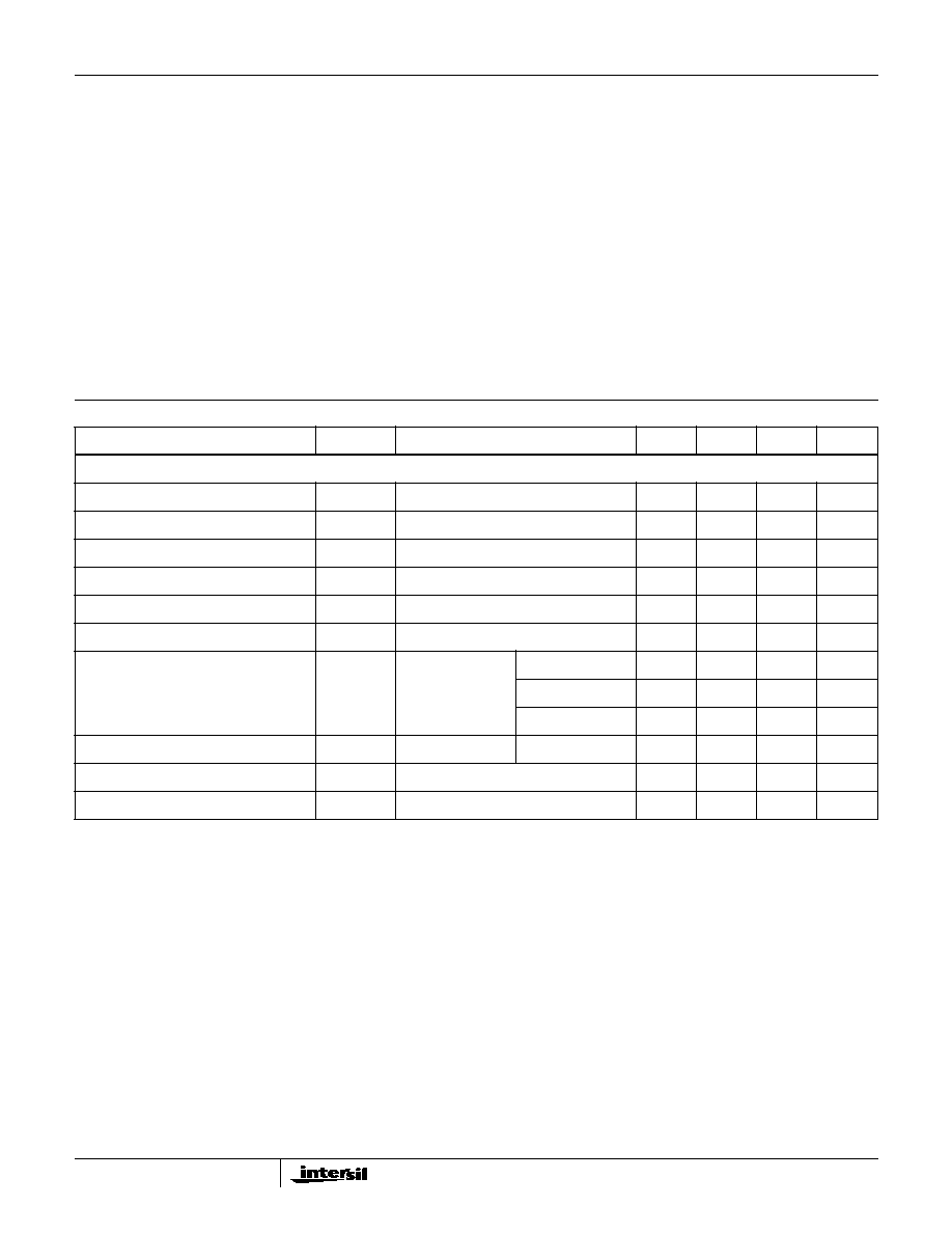
Absolute Maximum Ratings
Thermal Information
Collector to Emitter Voltage (V
CEO
). . . . . . . . . . . . . . . . . . . . . . . 8V
Collector to Base Voltage (V
CBO
) . . . . . . . . . . . . . . . . . . . . . . . 12V
Collector to Substrate Voltage (V
CIO
, Note 1) . . . . . . . . . . . . . . 20V
Collector Current (I
C
) . . . . . . . . . . . . . . . . . . . . . . . . . . . . . . . . 20mA
Operating Conditions
Temperature Range . . . . . . . . . . . . . . . . . . . . . . . . . -55
o
C to 125
o
C
Thermal Resistance (Typical, Note 2)
JA
(
o
C/W)
16 Ld PDIP Package . . . . . . . . . . . . . . . . . . . . . . . .
90
16 Ld SOIC Package . . . . . . . . . . . . . . . . . . . . . . . .
185
Maximum Power Dissipation (Any One Transistor) . . . . . . . . 85mW
Maximum Junction Temperature (Die) . . . . . . . . . . . . . . . . . . 175
o
C
Maximum Junction Temperature (Plastic Package) . . . . . . . . 150
o
C
Maximum Storage Temperature Range . . . . . . . . . . -65
o
C to 150
o
C
Maximum Lead Temperature (Soldering 10s) . . . . . . . . . . . . 300
o
C
(SOIC - Lead Tips Only)
CAUTION: Stresses above those listed in "Absolute Maximum Ratings" may cause permanent damage to the device. This is a stress only rating and operation of the
device at these or any other conditions above those indicated in the operational sections of this specification is not implied.
NOTES:
1. The collector of each transistor of these devices is isolated from the substrate by an integral diode. The substrate (Terminal 5) must be connected
to the most negative point in the external circuit to maintain isolation between transistors and to provide for normal transistor action.
2.
JA
is measured with the component mounted on an evaluation PC board in free air.
Electrical Specifications
T
A
= 25
o
C
PARAMETER
SYMBOL
TEST CONDITIONS
MIN
TYP
MAX
UNITS
DC CHARACTERISTICS FOR EACH TRANSISTOR
Collector to Base Breakdown Voltage
V
(BR)CBO
I
C
= 10
µ
A, I
E
= 0
12
20
-
V
Collector to Emitter Breakdown Voltage
V
(BR)CEO
I
C
= 1mA, I
B
= 0
8
10
-
V
Collector to Substrate Breakdown Voltage V
(BR)CIO
I
C1
= 10
µ
A, I
B
= 0, I
E
= 0
20
-
-
V
Emitter Cutoff Current (Note 3)
I
EBO
V
EB
= 4.5V, I
C
= 0
-
-
10
µ
A
Collector Cutoff Current
I
CEO
V
CE
= 5V, I
B
= 0
-
-
1
µ
A
Collector Cutoff Current
I
CBO
V
CB
= 8V, I
E
= 0
-
-
100
nA
DC Forward Current Transfer Ratio
h
FE
V
CE
= 6V
I
C
= 10mA
-
110
-
I
C
= 1mA
40
150
-
I
C
= 0.1mA
-
150
-
Base to Emitter Voltage
V
BE
V
CE
= 6V
I
C
= 1mA
0.62
0.71
0.82
V
Collector to Emitter Saturation Voltage
V
CE SAT
I
C
= 10mA, I
B
= 1mA
-
0.13
0.50
V
Base to Emitter Saturation Voltage
V
BE SAT
I
C
= 10mA, I
B
= 1mA
0.74
-
0.94
V
NOTE:
3. On small-geometry, high-frequency transistors, it is very good practice never to take the Emitter Base Junction into reverse breakdown. To do
so may permanently degrade the h
FE
. Hence, the use of I
EBO
rather than V
(BR)EBO
. These devices are also susceptible to damage by
electrostatic discharge and transients in the circuits in which they are used. Moreover, CMOS handling procedures should be employed.
CA3227
3
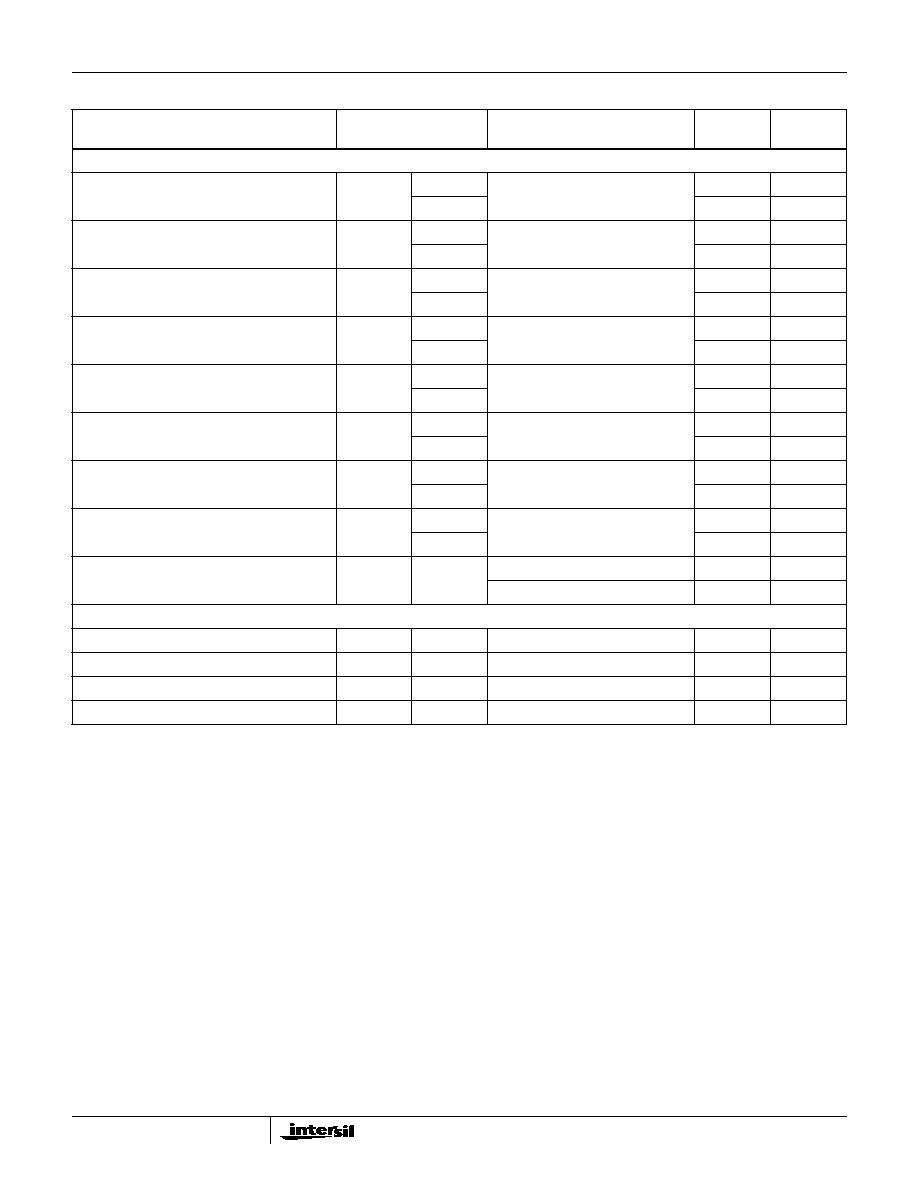
Electrical Specifications
T
A
= 25
o
C, 200MHz, Common Emitter, Typical Values Intended Only for Design Guidance
PARAMETER
SYMBOL
TEST CONDITIONS
TYPICAL
VALUES
UNITS
DYNAMIC CHARACTERISTICS FOR EACH TRANSISTOR
Input Admittance
Y
11
b
11
I
C
= 1mA, V
CE
= 5V
4
mS
g
11
0.75
mS
Output Admittance
Y
22
b
22
I
C
= 1mA, V
CE
= 5V
2.7
mS
g
22
0.13
mS
Forward Transfer Admittance
Y
21
Y
21
I
C
= 1mA, V
CE
= 5V
29.3
mS
21
-33
Degrees
Reverse Transfer Admittance
Y
12
Y
12
I
C
= 1mA, V
CE
= 5V
0.38
mS
12
-97
Degrees
Input Admittance
Y
11
b
11
I
C
= 10mA, V
CE
= 5V
4.8
mS
g
11
2.85
mS
Output Admittance
Y
22
b
22
I
C
= 10mA, V
CE
= 5V
2.75
mS
g
22
0.9
mS
Forward Transfer Admittance
Y
21
Y
21
I
C
= 10mA, V
CE
= 5V
95
mS
21
-62
Degrees
Reverse Transfer Admittance
Y
12
Y
12
I
C
= 10mA, V
CE
= 5V
0.39
mS
12
-97
Degrees
Small Signal Forward Current Transfer Ratio
h
21
I
C
= 1mA, V
CE
= 5V
7.1
I
C
= 10mA, V
CE
= 5V
17
TYPICAL CAPACITANCE AT 1MHz, THREE-TERMINAL MEASUREMENT
Collector to Base Capacitance
C
CB
V
CB
= 6V
0.3
pF
Collector to Substrate Capacitance
C
CI
V
CI
= 6V
1.6
pF
Collector to Emitter Capacitance
C
CE
V
CE
= 6V
0.4
pF
Emitter to Base Capacitance
C
EB
V
EB
= 3V
0.75
pF
Spice Model
(Spice 2G.6)
.model NPN
+
BF = 2.610E + 02
BR = 4.401E + 00
IS = 6.930E - 16
RB = 130.0E + 00
+
RC = 1.000E + 01
RE = 7.396E - 01
VA = 6.300E + 01
VB = 2.208E + 00
+
IK = 1.000E - 01
ISE = 1.87E - 14
NE = 1.653E + 00
IKR = 1.000E - 02
+
ISC = 9.25E - 14
NC = 1.333E + 00
TF = 1.775E - 11
TR = 1.000E - 09
+
CJS = 1.800E - 12
CJE = 1.010E - 12
PE = 8.350E - 01
ME = 4.460E - 01
+
CJC = 9.100E - 13
PC = 3.850E - 01
MC = 2.740E - 01
KF = 0.000E + 00
+
AF = 1.000E + 00
EF = 1.000E + 00
FC = 5.000E - 01
PJS = 5.410E - 01
+
MJS = 3.530E - 01
RBM = 30.00
RBV = 100
IRB = 0.00
Please Note: No measurements have been made to model the reverse AC operation (tr is an estimation).
CA3227

