 | –≠–ª–µ–∫—Ç—Ä–æ–Ω–Ω—ã–π –∫–æ–º–ø–æ–Ω–µ–Ω—Ç: CA3262A | –°–∫–∞—á–∞—Ç—å:  PDF PDF  ZIP ZIP |
1
August 1997
CA3262A, CA3262
Quad-Gated, Inverting Power Drivers
Features
∑ Independent Over-Current Limiting On Each Output
∑ Independent Over-Temperature Limiting On Each Output
∑ Output Drivers Capable of Switching 700mA Load
∑ Inputs Compatible With TTL or 5V CMOS Logic
∑ Suitable For Resistive, Lamp or Inductive Loads
∑ Power-Frame Package Construction For Good Heat
Dissipation
∑ Operating Temperature Ranges
- CA3262A . . . . . . . . . . . . . . . . . . . . . . . -40
o
C to 125
o
C
- CA3262 . . . . . . . . . . . . . . . . . . . . . . . . . -40
o
C to 85
o
C
Applications
System Applications
∑ Solenoids
∑
Automotive
∑ Relays
∑
Appliances
∑ Lamps
∑
Industrial Controls
∑ Steppers
∑
Robotics
∑ Small Motors
∑ Displays
Description
The CA3262 and CA3262A are used to interface low-level
logic to high current loads. Each Power Driver has four
inverting switches consisting of a non-inverting logic input
stage and an inverting low-side driver output stage. All inputs
are 5V TTL/CMOS logic compatible and have a common
Enable input. Each output device has independent current
limiting (I
LIM
) and thermal limiting (T
LIM
) for protection from
over-load conditions. Steering diodes connected from each
output (in pairs) to the Clamp pins may be used in
conjunction with external zener diodes to protect the IC
against over-voltage transients that result from inductive load
switching.
To allow for maximum heat transfer from the chip, all ground
pins on the DIP, PLCC and SOIC packages are directly
connected to the mounting pad of the chip. Integral heat
spreading lead frames directly connect the bond pads and
ground leads to conduct heat from the chip junction to the
PC Board for good heat dissipation.
The CA3262 and CA3262A can drive four incandescent
lamp loads without modulating their brilliance when the
"cold" lamps are energized. Outputs may be parallel
connected to drive high current loads. The maximum output
current of each output is determined by the over-current lim-
iting threshold which is typically 1.2A but may be as low as
0.7A.
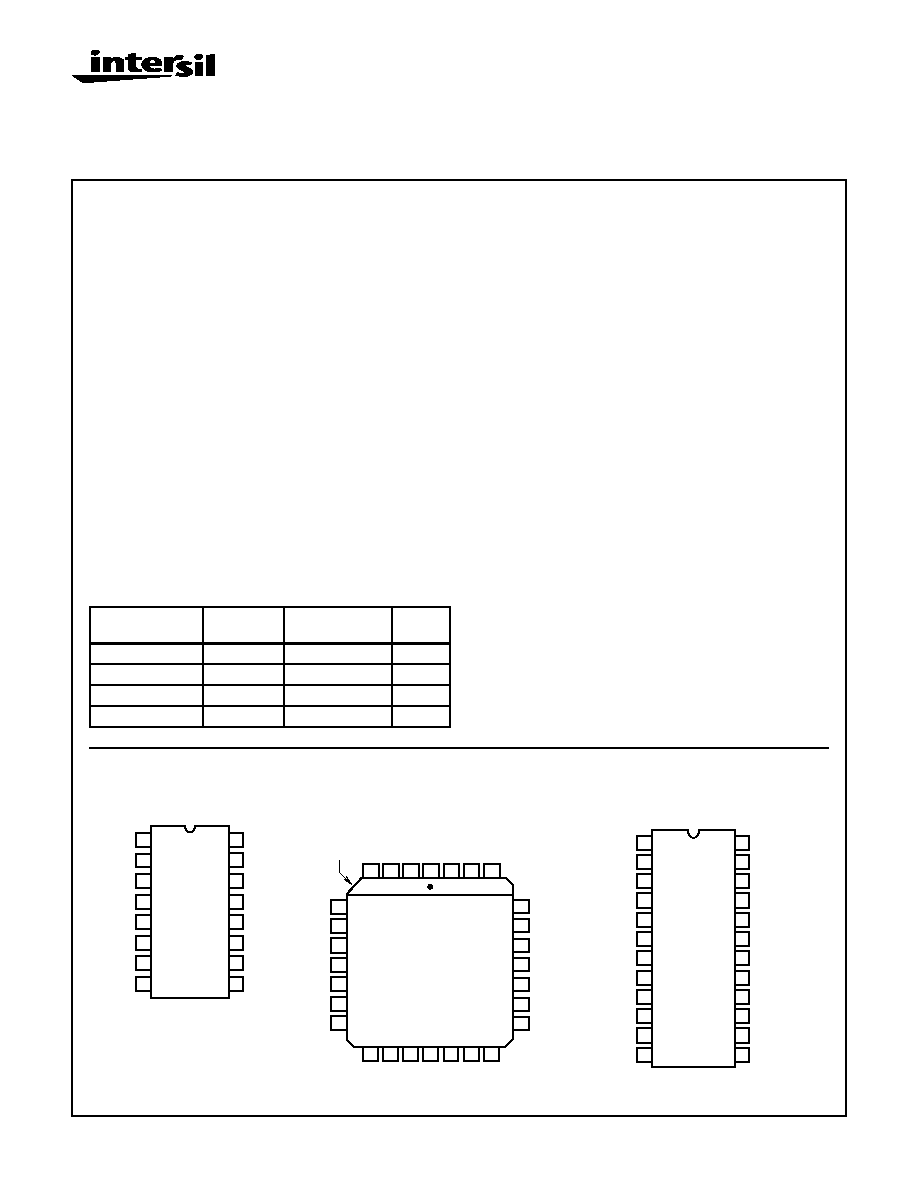
Pinouts
Ordering Information
PART NUMBER
TEMP.
RANGE (
o
C)
PACKAGE
PKG.
NO.
CA3262E
-40 to 85
16 Ld PDIP
E16.3
CA3262AE
-40 to 125
16 Ld PDIP
E16.3
CA3262AQ
-40 to 125
28 Ld PLCC
N28.45
CA3262AM
-40 to 125
24 Ld SOIC (W)
M24.3
CA3262, CA3262A (PDIP)
TOP VIEW
CA3262A (PLCC)
TOP VIEW
CA3262A (SOIC)
TOP VIEW
PRELIMINARY
14
15
16
9
13
12
11
10
1
2
3
4
5
7
6
8
OUT A
CLAMP
OUT B
GND
GND
OUT C
CLAMP
OUT D
IN A
IN B
ENABLE
GND
GND
V
CC
IN C
IN D
INDEX
OUT D
NC
IN D
IN C
V
CC
OUT C
CLAMP
OUT A
NC
IN A
IN B
ENABLE
OUT B
CLAMP
1
2
3
4
5
6
7
8
9
10
11
12 13 14 15 16 17 18
19
20
21
22
23
24
25
26
27
28
GND
GND
GND
GND
GND
GND
GND
GND
GND
GND
GND
GND
GND
GND
OUT A
CLAMP
OUT B
NC
GND
GND
GND
GND
NC
OUT C
CLAMP
OUT D
IN A
ENABLE
NC
GND
GND
GND
V
CC
IN C
IN D
IN B
GND
NC
1
2
3
4
5
6
7
8
9
10
11
12
16
17
18
19
20
21
22
23
24
15
14
13
File Number
1836.6
2
Functional Block Diagram
TRUTH TABLE (Each Output)
ENABLE
IN
OUT
H
H
L
H
L
H
L
X
H
H = High, L = Low, X = Don't Care
T
LIM
I
LIM
V
CC
IN D
IN B
IN A
IN C
OUT D
OUT C
CLAMP
ENABLE
T
LIM
I
LIM
V+
T
LIM
I
LIM
OUT B
OUT A
CLAMP
T
LIM
I
LIM
CONSTANT
CURRENT
SOURCES
V
CC
TO SUBSEQUENT STAGES
REFERENCE
VOLTAGE
1.2V
INPUT
ENABLE
FIGURE 1. CA3262A EQUIVALENT SCHEMATIC OF ONE
INPUT STAGE
I
LIM
I
LIM
I
LIM
I
LIM
T
LIM
T
LIM
T
LIM
T
LIM
V+
IN A
IN B
ENABLE
IN C
IN D
V
CC
OUT D
OUT C
CLAMP
OUT B
OUT A
CLAMP
SOLENOID
LAMP
V
BATT
V
BATT
HIGH CURRENT
TTL OR
CMOS
LOGIC
LEVEL
INPUTS
+5V P.S.
MOTOR
HIGH SIDE DR
RELAY
V
BATT
FIGURE 2. QUAD INVERTING POWER DRIVER (QDR) SHOWN WITH TYPICAL APPLICATION LOADS
CA3262A, CA3262
3
Absolute Maximum Ratings
Thermal Information
Logic Supply Voltage, V
CC
. . . . . . . . . . . . . . . . . . . . . . . . . . . . . . 7V
Logic Input Voltage, V
IN
. . . . . . . . . . . . . . . . . . . . . . . . . . . . . . . 15V
Output Voltage, V
CEX
. . . . . . . . . . . . . . . . . . . . . . . . . . . . . . . . . 60V
Output Sustaining Voltage, V
CE(SUS)
. . . . . . . . . . . . . . . . . . . . 40V
Output Transient Current . . . . . . . . . . . . . . . . . . . . . . . . . . (Note 1)
Output Load Current. . . . . . . . . . . . . . . . . . . . . . . . . . . . . . (Note 2)
Operating Conditions
Temperature Range
CA3262AE, CA3262AQ, CA3262AM . . . . . . . . . . -40
o
C to 125
o
C
CA3262E. . . . . . . . . . . . . . . . . . . . . . . . . . . . . . . . . -40
o
C to 85
o
C
Thermal Resistance (Typical, Note 3)
JA
(
o
C/W)
For PC Mount Without Added Copper Ground Area
CA3262E (PDIP) . . . . . . . . . . . . . . . . . . . . . . . . .
60
CA3262AE (PDIP) . . . . . . . . . . . . . . . . . . . . . . . .
60
CA3262AQ (PLCC) . . . . . . . . . . . . . . . . . . . . . . .
45
CA3262AM (SOIC) . . . . . . . . . . . . . . . . . . . . . . .
60
For PC Mount With 2 sq. in. of Added Copper Ground Area
CA3262E (PDIP) . . . . . . . . . . . . . . . . . . . . . . . . .
40
CA3262AE (PDIP) . . . . . . . . . . . . . . . . . . . . . . . .
40
CA3262AQ (PLCC) . . . . . . . . . . . . . . . . . . . . . . .
36
CA3262AM (SOIC) . . . . . . . . . . . . . . . . . . . . . . .
36
See Maximum Power Dissipation vs Temperature curves, Figures
6A and 6B.
Maximum Junction Temperature . . . . . . . . . . . . . . . . . . . . . . . 150
o
C
Maximum Storage Temperature Range . . . . . . . . . .-65
o
C to 150
o
C
Maximum Lead Temperature (Soldering 10s) . . . . . . . . . . . . . 265
o
C
CAUTION: Stresses above those listed in "Absolute Maximum Ratings" may cause permanent damage to the device. This is a stress only rating and operation
of the device at these or any other conditions above those indicated in the operational sections of this specification is not implied.
Electrical Specifications
V
CC
= 5.5V, T
A
= -40
o
C to 125
o
C for CA3262A and V
CC
= 5.5V, T
A
= -40
o
C to 85
o
C for CA3262
Unless Otherwise Specified
PARAMETER
SYMBOL
TEST CONDITIONS
CA3262
CA3262A
UNITS
MIN
TYP
MAX
MIN
TYP
MAX
Output Leakage Current
I
CEX
V
CE
= 60V, V
ENABLE
= 0.8V
-
-
100
-
0.6
50
µ
A
Output Sustaining
Voltage
V
CE(SUS)
Note 5
40
-
-
40
-
-
V
Collector Emitter
Saturation Voltage
(See Figures 4B and 5B)
V
CE(SAT)
V
IN
= 2V, V
CC
= 4.75V
I
C
= 100mA
-
-
0.25
-
0.05
0.15
V
I
C
= 200mA
-
-
-
-
-
0.2
V
I
C
= 300mA
-
-
-
-
-
0.25
V
I
C
= 400mA
-
-
0.4
-
0.2
0.3
V
I
C
= 500mA
-
-
-
-
-
0.4
V
I
C
= 600mA
-
-
0.6
-
-
0.5
V
I
C
= 700mA, T
A
= -40
o
C
-
-
0.6
-
-
0.5
V
Input Low Voltage
V
IL
-
-
0.8
-
-
0.8
V
Input High Voltage
V
IH
2
-
-
2
-
-
V
Input Low Current
I
IL
V
IN
= 0.8V
-
-
10
-
0.75
10
µ
A
Input High Current
I
IH
V
IN
= V
ENABLE
= 5.5V,
I
C
= 600mA
-
-
10
-
-
10
µ
A
Supply Current,
All Outputs ON,
(See Figures 4A and 5A)
I
CC(ON)
V
IN
= 2V, V
ENABLE
= 5.5V,
I
OUTA
= 250mA, I
OUTB
= 250mA,
I
OUTC
= 250mA, I
OUTD
= 250mA
-
-
70
-
(Note 4)
55
mA
Supply Current, All
Outputs OFF,
(See Figures 4A and 5A)
I
CC(OFF)
V
IN
= 0V
-
-
5
-
(Note 4)
5
mA
Clamp Diode Leakage
Current
I
R
V
R
= 60V
-
-
100
-
-
50
µ
A
Clamp Diode Forward
Voltage,
(See Figures 4D and 5D)
V
F
I
F
= 1A, V
IN
= 0V
-
-
1.7
-
-
1.7
V
I
F
= 1.5A, V
IN
= 0V
-
-
2.1
-
-
2.1
V
Turn-On Delay,
(See Figures 4C and 5C)
t
PHL
, t
PLH
I
OUT
= 500mA
-
-
8
-
-
8
µ
s
Over Current Limiting
I
LIM
V
OUT
= 2V, V
IN
= 5.5V,
V
ENABLE
= 5.5V
0.7
-
(Note 1)
0.7
-
(Note 1)
A
DESIGN PARAMETERS
Over Temperature Limiting
(Junction Temperature)
T
LIM
-
155
-
-
155
-
o
C
CA3262A, CA3262
4
Applications
Typical circuit configurations for applying the CA3262 and
CA3262A are shown in the application circuit of Figure 2. To
their rated capabilities, both circuits can be used to drive induc-
tive, resistive and lamp loads. The CA3262A has a lower V
SAT
than the CA3262 and is rated for 125
o
C ambient temperature
applications. The CA3262 data sheet rating is 85
o
C. Otherwise,
the protection features described apply to both the CA3262 and
CA3262A.
The maximum voltage for full load current switching is the
output sustaining voltage, V
CE(SUS)
which should not exceed
40V. To provide a means of over-voltage protection, on-chip
steering diodes are connected from each output to one of two
CLAMP pins. Over-voltage pulses may be generated from
inductive load switching and must be clamped or limited to a
peak voltage less than V
CE(SUS)
. To limit an inductive voltage
pulse, a zener diode should be connected to the appropriate
CLAMP pin. When the voltage pulse exceeds the zener thresh-
old, the excess energy is dumped to ground via the on-chip
steering diode and the external zener diode.
The on-chip diodes may be used in a free-wheeling mode by
connecting the CLAMP pins to an external clamp supply
voltage. Zener diode clamp protection is preferred over the
power supply clamp option, primarily because the power
supplies may be subject to large transient changes; including
turn-ON and turn-OFF conditions where non-tracking conditions
between supplies could allow forward conduction through the
steering diodes. For all transient conditions of either method, the
clamp voltage should greater than the maximum supply voltage
of the switching outputs and less than V
CE(SUS)
.
Note that the rate of change of the output current during load
switching is fast. Therefore, even small values of inductance,
including the inductance of a few meters of hook-up wire to
the load circuit, can generate voltage spikes of considerable
amplitude at the output terminals and may require clamping
to protect the device ratings.
Current-limiting is provided as protection for shorted or over-
loaded output conditions. Voltage is sampled across a small
metal resistor in the emitter of each output stage. When the volt-
age exceeds a preset comparator level, drive is reduced to the
output. Current limiting is sustained unless thermal conditions
exceed the preset thermal shutdown temperature of 155
o
C.
If an output is shorted, the remaining three outputs will
continue to function normally unless the continued heat
spreading is sufficient to raise the junction temperature at any
other output to a level greater than 155
o
C. High ambient tem-
perature conditions may allow this to happen. The degree of
interaction is minimized at chip layout design by separating
the output devices, each to a separate corner of the chip.
As noted, the thermal resistance values of the PDIP, PLCC
and SOIC packages are improved by direct connection of
the leads to the chip mounting pad. For a normal PC Board
application, the thermal resistance coefficient for each pack-
age can be significantly lowered by increasing ground cop-
per area on the PC board next to the ground pins of the IC.
Input Capacitance, Input
C
IN
-
-
-
-
3
-
pF
Enable Capacitance
C
EN
-
-
-
-
4.4
-
pF
NOTES:
1. The CA3262 and CA3262A have on-chip limiting for transient peak currents. Under short-circuit conditions with voltage applied to the collector
of the output transistor and with the output transistor turned ON, the current will increase to 1.2A, typical. Over-Current Limiting protects a short
circuit condition for a normal operating range of output supply voltage. During a short circuit condition, the output driver will shortly thereafter
(approx. 5ms) go into Over-Temperature Limiting. While Over-Current Limiting may range to peak currents greater than 2A, each output will
typically withstand a direct short circuit up to supply voltage levels of 16V. Excessive dissipation before thermal limiting occurs may cause dam-
age to the chip for supply voltages greater than 18V. The CA3262 and CA3262A are rated to withstand peak current, cold turn-on conditions of
#168 or #194 lamp loads.
2. The total DC current for the CA3262 and CA3262A with all 4 outputs ON should not exceed the total of (4 x 0.7A + Max. I
CC
) ~ 2.85A. This level
of current will significantly increase the chip temperature due to increased dissipation and may cause thermal shutdown in high ambient tem-
perature conditions (See Absolute Maximum Ratings for Dissipation). Any one output may be allowed to exceed 0.7A but may be subject to
Over-Current Limiting above the I
LIM
min. limit of 0.7A. As a practical limit, no single output should be loaded to more than 1A (Max).
3. Normal applications require a surface mount of the 28 lead PLCC and 24 lead SOIC packages on a PC Board. The PLCC, SOIC and PDIP
packages have power lead frame construction through the ground pins to conduct heat from the frame to the PC Board ground area. Thermal
resistance,
JA
, is given for a surface mount of the 28 lead PLCC and the 24 lead SOIC packages on a 1 oz. copper PC board with minimal
ground area and with 2 square inches of ground area.
4. I
CC
varies with temperature. Typically, I
CC(ON)
is 18mA at 125
o
C and 41mA at -40
o
C. Typically, I
CC(OFF)
is 2.2mA at 125
o
C and 1.2mA at
-40
o
C.
5. Tested with a switched-off 500mA Load of 120mH (with 24
series resistance), V
BATT
= 12V and the outputs (V
CE
) clamped to +40V maximum
with an external zener diode.
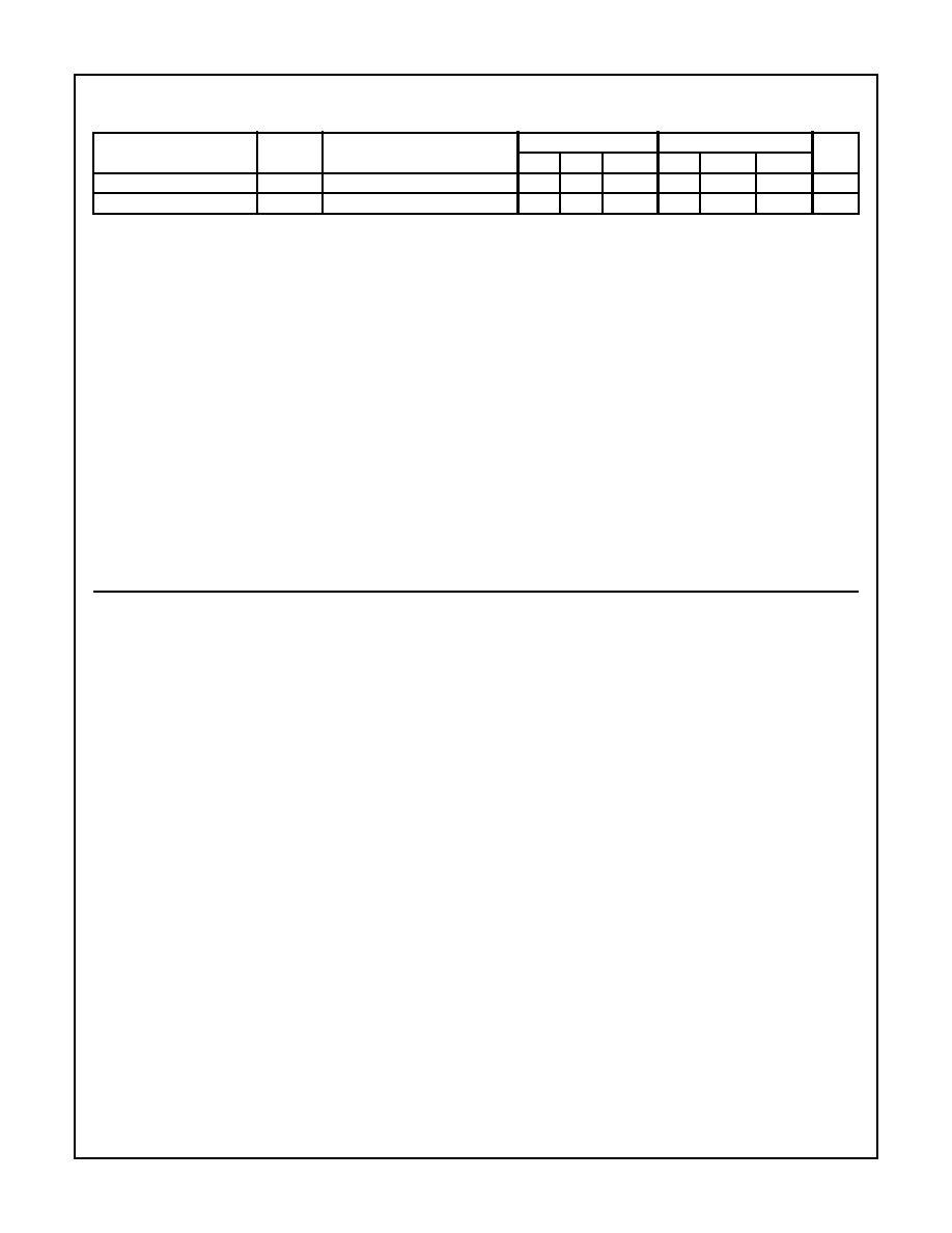
Electrical Specifications
V
CC
= 5.5V, T
A
= -40
o
C to 125
o
C for CA3262A and V
CC
= 5.5V, T
A
= -40
o
C to 85
o
C for CA3262
Unless Otherwise Specified (Continued)
PARAMETER
SYMBOL
TEST CONDITIONS
CA3262
CA3262A
UNITS
MIN
TYP
MAX
MIN
TYP
MAX
CA3262A, CA3262
5
Typical Performance Curves
FIGURE 4A. TYPICAL SUPPLY CURRENT (PIN 11)
CHARACTERISTICS
FIGURE 4B. TYPICAL COLLECTOR-TO-EMITTER SATURATION
VOLTAGE CHARACTERISTICS IN QUAD-GATED
INVERTING POWER DRIVER OUTPUT
FIGURE 4C. TYPICAL PROPAGATION DELAY TIME CHARAC-
TERISTICS
FIGURE 4D. TYPICAL CLAMP-DIODE FORWARD VOLTAGE
CHARACTERISTICS
FIGURE 4. TYPICAL CHARACTERISTICS OF THE CA3262E
CURRENT
AMPLIFIER
CURRENT
SENSE
TEMP.
SENSE
BANDGAP
VOLT. REF.
I
B
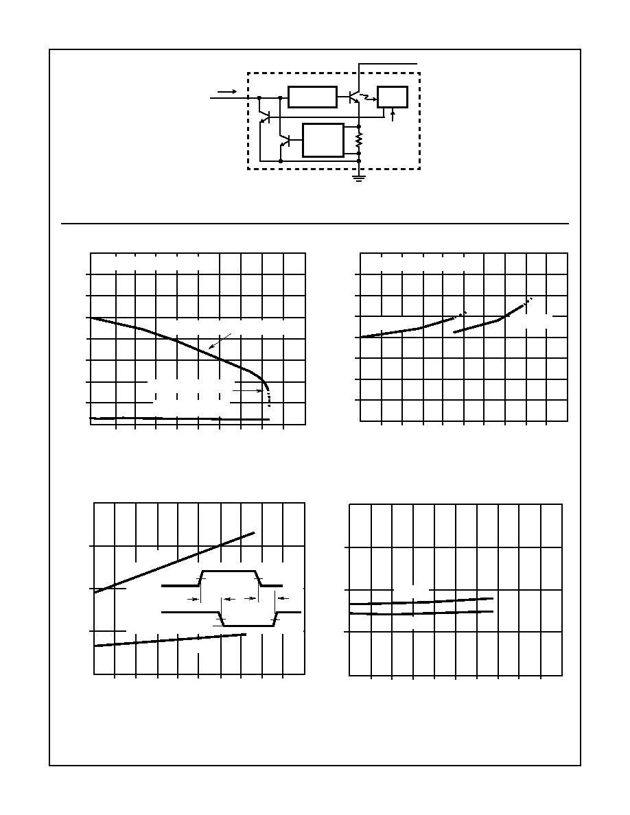
FIGURE 3. EACH OUTPUT POWER DRIVER IS A COMPOSITE CIRCUIT WITH OVER-TEMPERATURE SENSE FOR THERMAL
LIMITING AND OVER-CURRENT SENSE TO PROVIDE CURRENT LIMITING
80
70
60
50
40
30
20
10
0
SUPPLY VOLTAGE (V
CC
) = 5.5V
V
IN
= 2V, I
OUT
= 250mA (EACH)
-40
-20
0
20
40
60
80
100
120
AMBIENT TEMPERATURE (
o
C)
THERMAL SHUTDOWN
V
IN
= 0V, I
OUT
= 0mA
140
SUPPL
Y CURRENT (mA)
0.7
0.6
0.5
0.4
0.3
0.2
0.1
COLLECT
OR-T
O-EMITTER
-40
-20
0
20
40
60
80
100
120
SUPPLY VOLTAGE (V
CC
) = 4.75V
I
C
= 700mA
I
C
= 600mA
140
AMBIENT TEMPERATURE (
o
C)
SA
TURA
TION V
O
L
T
A
GE (V)
50%
50%
(OFF)
50%
50%
(ON)
t
PHL
t
PLH
V
OUT
1, 3, 6, 8
(2) (4) (12) (14)
V
IN
9, 10, 15, 16
(16) (17) (27) (28)
t
PHL
t
PLH
4
3
2
1
0
PR
OP
A
G
A
TION DELA
Y TIME (
µ
s)
-40
-20
0
20
40
60
80
100
120
AMBIENT TEMPERATURE (
o
C)
140
-40
-20
0
20
40
60
80
100
120
4
3
2
1
0
CLAMP DIODE FOR
W
ARD V
O
L
T
A
GE (V)
I
F
= 1.5A
I
F
= 1A
140
AMBIENT TEMPERATURE (
o
C)
CA3262A, CA3262