 | –≠–ª–µ–∫—Ç—Ä–æ–Ω–Ω—ã–π –∫–æ–º–ø–æ–Ω–µ–Ω—Ç: CA3272A | –°–∫–∞—á–∞—Ç—å:  PDF PDF  ZIP ZIP |
1
July 1997
CA3272A, CA3292A
Quad-Gated Inverting Power Drivers with Fault
Mode Diagnostic Flag Output
Features
∑ Load Current Switching 600mA
∑ Suitable for Resistive or Inductive Loads
∑ Fault Mode Diagnostic Flag Output
∑ CA3292A Over-Voltage Zener Clamp
∑ Independent Over-Current Limiting
∑ Independent Over-Temperature Shutdown
∑ Temperature Shutdown Hysteresis
∑ 5V CMOS or TTL Input Logic
∑ High Dissipation Power-Frame Package
∑ Operating Temperature Range -40
o
C to 125
o
C
Description
The CA3272A and CA3292A are Quad-Gated Inverting Power
Drivers for interfacing low-level logic to inductive and resistive
loads such as: relays, solenoids, AC and DC motors and resis-
tive loads such as incandescent lamps and other power drivers.
Each output is an open collector protected power transistor
driver. The CA3292A is similar to the CA3272A, except for an
added collector-to-base Zener diode that provides over-voltage
clamping protection on each power switching output. The
CA3292A block diagram is shown for one switching channel
with fault detection logic plus the output fault driver circuit for all
four switching channels. The FAULT output pin provides a flag
output when a fault condition occurs. All four Output Power
Driver stages are shown in the Block Diagrams.
The ENABLE input is common to each of the four power
switches and when low, disables the FAULT output. From the
Input to Output, each switch is inverting. When IN is high, OUT
is low and the transistor switch is "ON" (conducting). The block
diagram shows the functional logic associated with fault detec-
tion. The Fault Sense circuit detects the IN and OUT states and
switches Q
F
"ON" if a fault is detected. When a fault is detected,
transistor Q
F
activates a current sink pull-down at the FAULT
pin. A resistive load from the FAULT pin to the power supply is
used to detect a fault as a low state. Both shorted and open
load conditions are detected.
Note: The CA3272A replaces the CA3272 for new designs.
Refer to the Fault Sink Current specifications when making
design changes. The CA3272A and CA3292A have increased
pull-down current drive from the FAULT output pin.
Pinouts
Applications
System Applications
∑ Solenoids
∑ Automotive
∑ Relays
∑ Appliance
∑ Lamps
∑ Industrial Control
∑ Steppers
∑ Robotics
∑ Injectors
∑ Motors
Ordering Information
PART NUMBER
TEMP.
RANGE (
o
C)
PACKAGE
PKG.
NO.
CA3272AQ
-40 to 125
28 Ld PLCC
N28.45
CA3292AQ
-40 to 125
28 Ld PLCC
N28.45
CA3272AM
-40 to 125
28 Ld SOIC
M28.3
CA3292AM
-40 to 125
28 Ld SOIC
M28.3
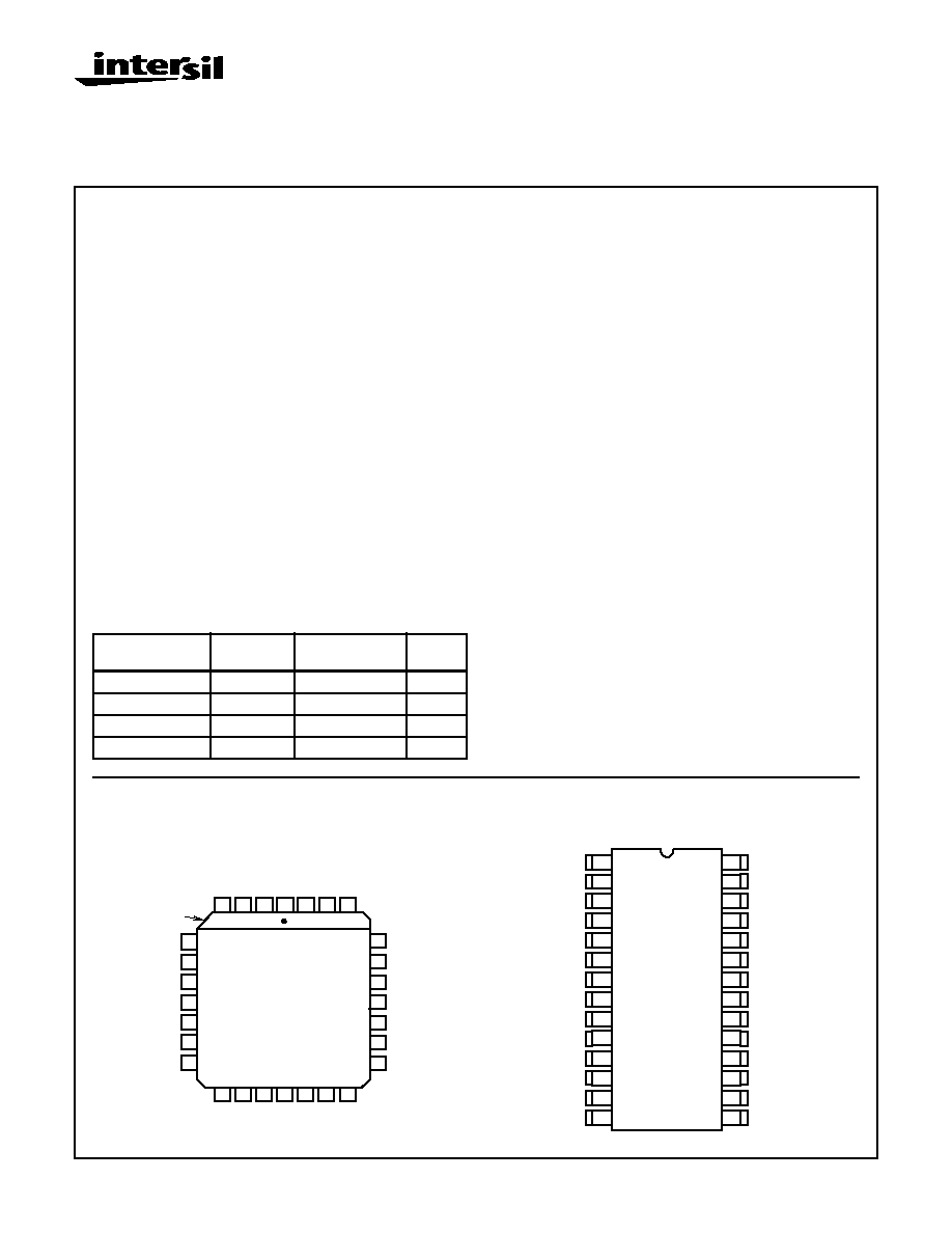
CA3272A, CA3292A (PLCC)
TOP VIEW
CA3272A, CA3292A (SOIC)
TOP VIEW
INDEX
OUT D
NC
IN D
IN C
V
CC
OUT C
NC
OUT A
F
A
UL
T
IN A
IN B
ENABLE
OUT B
NC
1
2
3
4
5
6
7
8
9
10
11
12 13 14 15 16 17 18
19
20
21
22
23
24
25
26
27
28
GND
GND
GND
GND
GND
GND
GND
GND
GND
GND
GND
GND
GND
GND
1
2
3
4
5
6
7
8
9
10
11
12
OUT B
NC
NC
NC
NC
GND
GND
GND
GND
NC
NC
NC
20
21
22
23
24
25
26
27
28
19
18
17
OUT A
IN A
IN B
ENABLE
GND
GND
NC
V
CC
IN C
FAULT
GND
GND
13
14
NC
OUT C
16
15
IN D
OUT D
File Number
2223.7
CAUTION: These devices are sensitive to electrostatic discharge; follow proper IC Handling Procedures.
http://www.intersil.com or 407-727-9207
|
Copyright
©
Intersil Corporation 1999

2
Block Diagram of the CA3272A
Block Diagram of the CA3292A
(1 of 4 Outputs Shown with Expanded Fault Logic)
NOTE: The CA3292A is identical to the CA3272A except for the
collector-to-base Zener diode on each low side power output driver
(shown here as Z
A
). The Zener diode clamp is used as an over-
voltage clamp to protect the output when switching inductive loads.
When the output voltage exceeds the Zener threshold, Q
A
conducts
to suppress further increase in output voltage. The fault sense and
fault flag logic circuits are the same in the CA3272A and CA3292A.
F
T
LIM
I
LIM
OUT A
Q
A
0.02
F
T
LIM
I
LIM
OUT D
FAULT
IN A
IN B
IN C
IN D
ENABLE
V
CC
Q
D
0.02
F
T
LIM
I
LIM
OUT C
Q
C
0.02
F
T
LIM
I
LIM
OUT B
Q
B
0.02
TRUTH TABLE
ENABLE
IN
OUT
H
H
L
H
L
H
L
X
H
H = High, L = Low, X = Don't Care
I
LIM
T
LIM
FAULT INPUT
FROM B, C, D
FAULT
FLAG LOGIC
FAULT SENSE
CHANNEL A
4V
Z
A
Q
A
OUT A
FAULT
Q
F
0.02
CHANNEL A
1 OF 4
OUTPUTS
IN A
ENABLE
ENABLE LINE
TO B, C AND D
INPUTS AND
FAULT OUTPUT
CHANNELS
CA3272A, CA3292A
3
Absolute Maximum Ratings
Thermal Information
Output Voltage, V
O
(CA3272A) . . . . . . . . . . . . . . . . . . . . . . . . +60V
Output Sustaining Voltage, V
CE(SUS)
(CA3272A) . . . . . . . . . . . 40V
Output Voltage, V
O
(CA3292A) . . . . . . . . . . . . . . . . . . . . . V
CLAMP
Maximum Output Clamp Energy (CA3292A) . . . . . . . . . . . (Note 8)
Output Transient Current, (Note 1) . . . . . . . . . . . . . . . . . . 1.6A Max.
Output Load Current, (Note 2) . . . . . . . . . . . . . . . . . . . . . . . . . . 0.7A
Supply Voltage, V
CC
. . . . . . . . . . . . . . . . . . . . . . . . . . . . . . . . . . +7V
Logic Input Voltage, V
IN
. . . . . . . . . . . . . . . . . . . . . . . . . . . . . . 15V
FAULT Output Voltage, V
F
. . . . . . . . . . . . . . . . . . . . . . . . . . . . . 16V
Operating Conditions
Temperature Range . . . . . . . . . . . . . . . . . . . . . . . . . -40
o
C to 125
o
C
Thermal Resistance (Typical, Note 3)
JA
(
o
C/W)
For surface mount without added copper ground area:
CA3272AQ, CA3292AQ (PLCC) . . . . . . . . . . . . . . 45
o
C/W
CA3272AM, CA3292AM (SOIC). . . . . . . . . . . . . . . 56
o
C/W
For surface mount with 2 sq. in. of added copper ground area:
CA3272AQ, CA3292AQ (PLCC) . . . . . . . . . . . . . . 36
o
C/W
CA3272AM, CA3292AM (SOIC). . . . . . . . . . . . . . . 35
o
C/W
See Maximum Power Dissipation vs Temperature Curves,
Figures 6 and 7.
Maximum Junction Temperature (Plastic Packages) . . . . . . . 150
o
C
Maximum Storage Temperature Range . . . . . . . . . .-65
o
C to 150
o
C
Maximum Lead Temperature (Soldering 10s) . . . . . . . . . . . . . 300
o
C
(SOIC, PLCC - Lead Tips Only)
CAUTION: Stresses above those listed in "Absolute Maximum Ratings" may cause permanent damage to the device. This is a stress only rating and operation
of the device at these or any other conditions above those indicated in the operational sections of this specification is not implied.
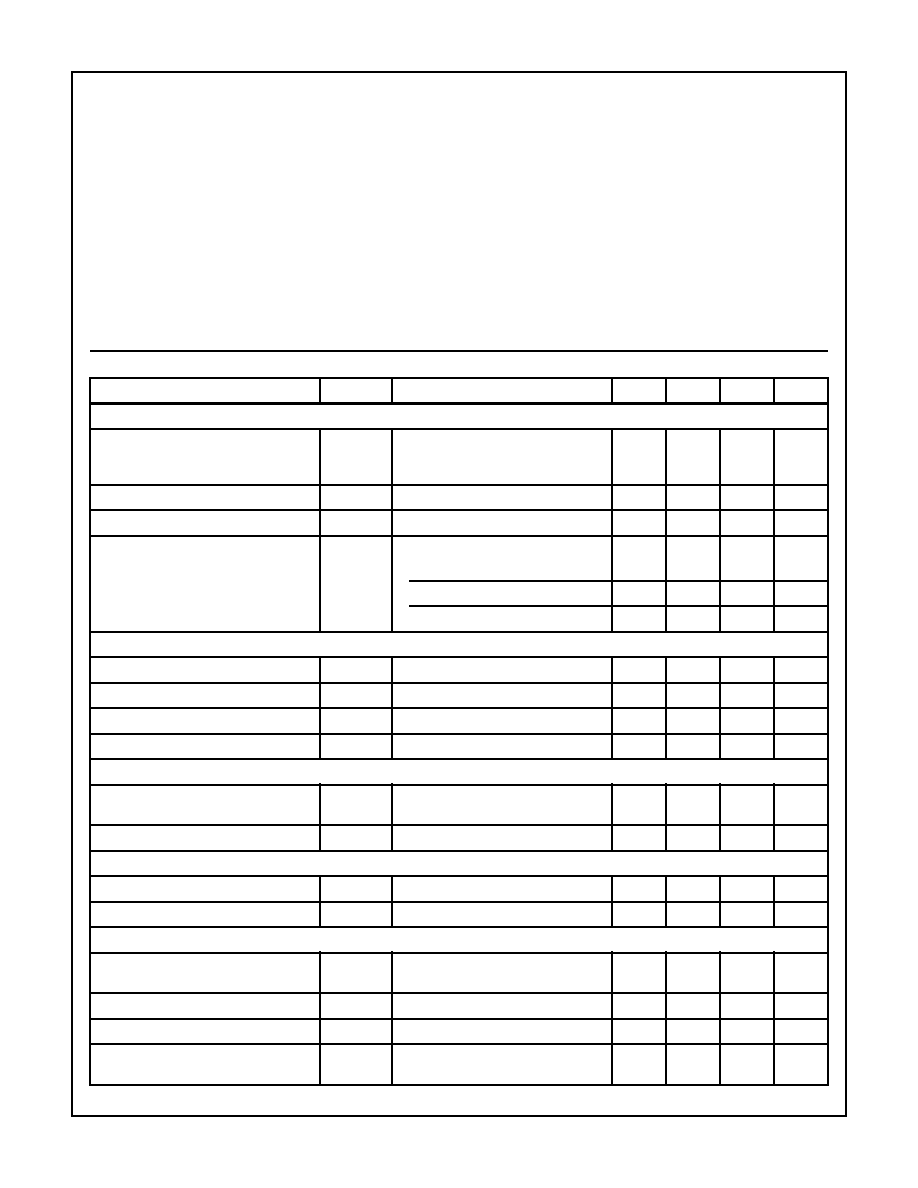
Electrical Specifications
T
A
= -40
o
C to 125
o
C, V
CC
= 5.5V, Unless Otherwise Specified
PARAMETER
SYMBOL
TEST CONDITIONS
MIN
TYP
MAX
UNITS
OUTPUT PARAMETERS
Output (OFF) Current
I
CEX
V
IN
= 0.8V; V
EN
= 5.5V; (Note 4)
V
CE
= 60V for CA3272A
V
CE
= 24V for CA3292A
-
30
100
µ
A
Output Sustaining Voltage: CA3272A
V
CE(SUS)
Note 7
40
-
-
V
Output Clamp Voltage: CA3292A
V
CLAMP
I
C
= 300
µ
A; V
EN
= 0.8V
28
32
36
V
Collector-to-Emitter Saturation Voltage
V
CE(SAT)
V
IN
= 2V, V
CC
= 4.75V,
I
C
= 400mA, T
A
= 125
o
C
-
-
0.3
V
I
C
= 500mA, T
A
= 25
o
C
-
-
0.4
V
I
C
= 600mA, T
A
= -40
o
C
-
-
0.5
V
LOGIC INPUT THRESHOLDS
Input Low Voltage
V
IL
V
CC
= 3.5V
-
-
0.8
V
Input High Voltage
V
IH
2
-
-
V
Input Low Current
I
IL
V
IN
= V
EN
= 0.8V; V
CC
= 4.75V
10
45
70
µ
A
Input High Current
I
IH
V
IN
= V
EN
= 5.5V
10
45
70
µ
A
SUPPLY CURRENT
All Outputs ON
I
CC(ON)
V
IN
= V
EN
= 5.5V; I
OUTA
= I
OUTB
=
I
OUTC
= I
OUTD
= 400mA
-
-
65
mA
All Outputs OFF
I
CC(OFF)
V
IN
= 0V
-
-
10
mA
PROPAGATION DELAY
Turn-ON Delay
t
PHL
I
LOAD
= 500mA
-
3
10
µ
s
Turn-OFF Delay
t
PLH
I
LOAD
= 500mA
-
3
10
µ
s
FAULT PARAMETERS
Output Low Current, I
F(SINK)
(with Fault)
I
OL
V
IN
= 0.8V; V
EN
= 2.0V; V
F
= 4V
V
OUT
= Low = 1V; (Note 5)
1
2
4
mA
Output High Current, I
F(LK)
I
OH
No Fault (Note 5)
-
-
20
µ
A
Output Low Voltage
V
OL
External Load Equal Min. I
OL
-
0.2
0.4
V
Output Driver Fault Sense, High
Threshold (Open)
V
HTHD
V
IN
= 0.8V; V
EN
= 2V (Note 6)
3
4
5.5
V
CA3272A, CA3292A
4
Output Driver Fault Sense, Low Threshold
(Short)
V
LTHD
V
IN
= V
EN
= 2V (Note 6)
3
4
5.5
V
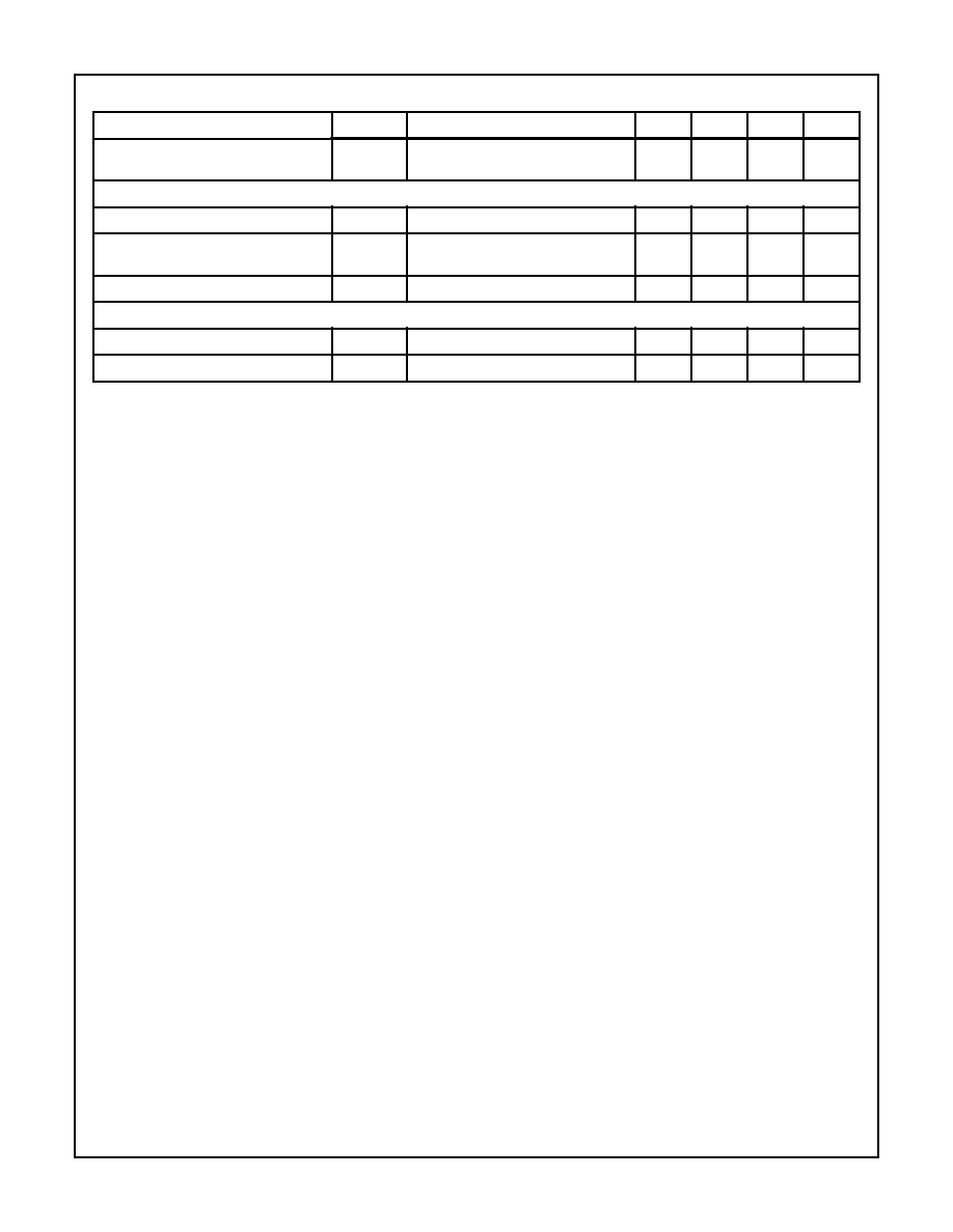
PROTECTION PARAMETERS
Over-Current Limiting
I
LIM
V
IN
= V
EN
= 2V, V
OUT
= 4
to 16V
0.7
-
Note 1
A
Over-Temperature Limiting
(Junction Temperature)
T
LIM
-
165
-
o
C
Over-Temperature Limiting, Hysteresis
T
HYS
-
15
-
o
C
DESIGN PARAMETERS
Input Capacitance
C
IN
-
3
-
pF
Enable Capacitance
C
EN
-
4.6
-
pF
NOTES:
1. Output Transient Currents are controlled by on-chip limiting for each output. Under short-circuit conditions with voltage applied to the
collector of the output transistor and with the output transistor turned ON, the current will increase to 1.2A, typical. Over-Current Limiting
protects a short circuit condition for a normal operating range of output supply voltage. During a short circuit condition, the output driver
will shortly thereafter (approximately 5ms) go into Over-Temperature Shutdown. While Over-Current Limiting may range to peak cur-
rents as high as 1.6A, each output will typically withstand a direct short circuit at normal single battery supply levels. Excessive dissi-
pation before thermal shutdown occurs may cause damage to the chip for supply voltages greater than 16V. When sequentially
switched, the outputs are rated to withstand peak current, cold turn-on conditions of lamp loads such as #168 or #194 lamps.
2. The total DC current with all 4 outputs ON should not exceed the total of (4 x 0.7A + Max. I
CC
)
~
2.85A. This level of current will signif-
icantly increase the chip temperature due to increased dissipation and may cause thermal shutdown in high ambient temperature con-
ditions (See Absolute Maximum Ratings for Dissipation). Any one output may be allowed to exceed 0.7A but may be subject to Over-
Current Limiting above the I
LIM
minimum limit of 0.7A. No single output should be loaded to more than Over-Current Limiting above
the I
LIM
minimum limit of 0.7A. As a practical limit, no single output should be loaded to more than 1A maximum.
3. The PLCC and SOIC packages have power lead frame construction through the ground pins to conduct heat from the frame to the PC
Board ground area. Thermal resistance,
JA
is given for a surface mount of the 28 lead PLCC and the 28 lead SOIC packages on a 1 oz.
copper PC board with minimal ground area and with a 2 square inches of ground area.
4. I
CEX
is the static leakage current at each output when that output is OFF (ENABLE Low). Refer to the Figure 3 illustration of an output
stage. The value of I
CEX
is both the leakage into the output driver and a pull-down current sink, I
O(SINK)
. The purpose of the current
sink is to detect open load conditions.
5. The I
OL
value of "Output Low Current, I
F(SINK)
" at the FAULT pin is both the static leakage of the output driver Q
F
and the current sink,
I
F(SINK)
. The current sink is active only when a fault exists. When no fault exists, the I
OH
current at the FAULT pin is the maximum
leakage current, I
F(LK)
. Refer to Figure 2 for an illustration of the FAULT output and associated external components. Refer to FAULT
LOGIC TABLE for Fault Modes.
6. The Voltages, V
HTHD
, V
LTHD
are the comparator threshold reference values (Min. and Max. Range) sensed as a high and low state
transitions for voltage forced at the outputs. V
HTHD
indicates an open load fault when the output is decreased to less than the threshold.
V
LTHD
indicates a shorted load when the output is increased greater than the threshold. The output voltage is changed until the FAULT
pin indicates a Low (Fault). Refer to Figure 2 for test value of external resistor. Refer to I
OL
and I
OH
FAULT PARAMETERS Test Limits
to determine V
OL
and V
OH
at the FAULT pin.
7. Tested with 120mA switched off in a Load of 70mH and 32
series resistance;
CA3272A: Outputs clamped with an external Zener diode, limiting V
OUT
to the V
CE(SUS)
maximum rating of +40V.
CA3292A: Outputs limited to the V
CLAMP
voltage by the internal collector-to-base Zener diode and output transistor clamp.
8. The single pulse clamp energy rating for the CA3292A is defined over a range of operating conditions. The Clamp Energy is a function
of the Load Inductance, Load Resistance, Clamp Voltage, Supply Voltage, the Saturated ON Resistance (V
SAT
) and the Steady State
Load Current at the instant of Turn-OFF. Refer to Figure 5 for the Safe Operating Area when driving inductive loads. Rating limits for
Energy vs Single Pulse Width Time are plotted for different coil values. Refer to Application Note - AN9416 for pulse energy calculation
methods.
Electrical Specifications
T
A
= -40
o
C to 125
o
C, V
CC
= 5.5V, Unless Otherwise Specified (Continued)
PARAMETER
SYMBOL
TEST CONDITIONS
MIN
TYP
MAX
UNITS
CA3272A, CA3292A

5
Applications
The CA3272A and CA3292A are quad-gated inverting low-
side power drivers with a fault diagnostic flag output. Both
circuits are rated for 125
o
C ambient temperature applica-
tions and have current limiting and thermal shutdown. While
functionally similar to the CA3262AQ, they differ in the mode
of over-voltage protection and have the added feature of a
FAULT flag output. Also, as shown in Figure 1, the inputs to
channels A, B, C, D and ENABLE have internal pulldowns to
turn "OFF" the outputs when the inputs are floating.
As noted in the Block Diagrams, the CA3292A is equivalent
to the CA3272A except that it has internal clamp diodes on
the outputs to handle inductive switching pulses from the
output load. The structure of each CA3292A output includes
a Zener diode from collector-to-base of the output transistor.
This is a different form of protection from other quad drivers
with current steering clamp diodes on each output, paired to
one of two "CLAMP" output pins. The CA3292A output tran-
sistor will turn-on at the Zener diode clamp voltage threshold
which is typically 32V and the output transistor will dump the
pulse energy through the output driver to ground.
Each output driver is capable of switching 600mA load currents
and operate at 125
o
C ambient temperature without interaction
between the outputs. The CA3272A and CA3292A can drive
four incandescent lamp loads without modulating their brilliance
when the "cold" lamps are energized. The outputs can be con-
nected in parallel to drive larger loads. Over-current or short cir-
cuit output load conditions are fault protected by current limiting
with a typical limit value of 1.2A. The current limiting range is
set for 0.6A to 1.6A. The output stage does not change state
(oscillate) when in the current limit mode.
Any one output that faults (see Fault Logic Table) will switch the
FAULT output at pin 1 to a constant current pull-down.
The Fault Logic circuit, as shown in the Block Diagram for
the CA3292A, applies to both the CA3272A and CA3292A.
The Fault Sense circuits do not override or control the power
switching circuits of the IC. Their primary function is to pro-
vide an external diagnostic fault flag output. Each Power
Switching Channel has diagnostic fault sensing input to the
Fault Logic. The Fault Logic block of the functional Block Dia-
gram illustrates the logic functions associated with Fault
detection. The diagnostic output for each of the four channels
of switching is processed through the fault logic circuit associ-
ated with each channel. It is then passed to an OR gate
which controls the FAULT flag output transistor, Q
F
thru A 2
input AND gate.
The ENABLE input is common to each of the 4 power
switches and also disables the FAULT flag output at the
2 input AND gate when it is low. The Fault Logic circuit
senses the IN and OUT states and switches Q
F
"ON" if a
fault is detected. Transistor Q
F
activates a sink current
source to pull-down the FAULT pin to a 0 (low) state when
the fault is detected. Both shorted and open load conditions
are detected.
It is normal for thermal shutdown and current limiting to
occur sequentially during a short circuit fault condition. A
precaution applies for potential damage from high transient
dissipation during thermal shutdown. (See Note 1 following
the Electrical Specifications Table).
Each of the outputs are independently protected with over-
current limiting and over-temperature shutdown with thermal
hysteresis. If an output is shorted, the remaining outputs
function normally unless the temperature rise of the other
output devices can be made to exceed their shutdown tem-
perature of 165
o
C typical. When the junction temperature of
a driver exceeds the 165
o
C thermal shutdown value, that
output is turned off. When an output is shutdown, the result-
ing decrease in power dissipation allows the junction tem-
perature to decrease. When the junction temperature
decreases by approximately 15
o
C, the output is turned on.
FAULT LOGIC TABLE
IN
OUT
FAULT
MODE
H
L
H
Normal
H
H
L
Over Current, Over Temperature Open
Load or Short to Power Supply
L
L
L
L
H
H
Normal
V
CC
REFERENCE
1.2 VOLTS
CONSTANT
CURRENT SOURCE
INPUT
TO PREDRIVER
AND
OUTPUT STAGES
ENABLE
FIGURE 1. SCHEMATIC OF ONE INPUT STAGE
FAULT
1
C
X
R
X
V
CC
= +5V
ENABLE IN
FAULT MODE
INPUT
CHANNEL "A"
T
X
= R
X
C
X
0.5 TO 1ms
Q
F
I
F(SINK)
LOGIC
OUTPUT
FAULT FLAG
DIAGNOSTIC
OUTPUT, V
F
B, C AND D
FAULT MODE
INPUTS
FIGURE 2. EXTERNAL FAULT OUTPUT CIRCUIT AND I
F(SINK)
AS FAULT SINK PULLDOWN CURRENT, WHICH IS
ACTIVATED BY TRANSISTOR, Q
F
, WHEN A FAULT
EXISTS
CA3272A, CA3292A