 | –≠–ª–µ–∫—Ç—Ä–æ–Ω–Ω—ã–π –∫–æ–º–ø–æ–Ω–µ–Ω—Ç: CA3274E | –°–∫–∞—á–∞—Ç—å:  PDF PDF  ZIP ZIP |
10-40
CAUTION: These devices are sensitive to electrostatic discharge; follow proper IC Handling Procedures.
http://www.intersil.com or 407-727-9207
|
Copyright
©
Intersil Corporation 1999
CA3274
Current Limiting Power Switch
with Current Limiter Sense Flag
Description
The CA3274 is a controlled current switch and may be used in
general purpose switching applications that require specified
maximum levels of current. The functional block diagram of
the CA3274 is shown and a typical application circuit is shown
in Figure 1. An internal emitter follower has 200mA of source
drive output capability. The Control Input is a Schmitt trigger
buffer amplifier for noise immunity in the environments typical
of industrial and automotive control systems.
Current sensing in the emitter circuit of a power-darlington
output stage is fed back from a sampling resistor to the sense
input of the CA3274 which has a 335mV typical offset. For the
example shown in Figure 1, a sampling resistor of 0.056
permits 6.0A (0.335/0.056) of current in the emitter of the output
driver. When the current limiter is activated, the flag output
changes state conditionally. If the control input is the "0" state,
the flag output will remain in a "1" state. If the control input is in
the "1" state and the sense input is less than the voltage
reference level of 335mV, the flag output will remain in the "1"
state. If the control input is the "1" state and the sense input is
equal to or greater than the 335mV reference level, the flag
output goes to the "0" state. The output flag switch may be used
to accurately establish dwell timing in automotive applications.
When the control input goes to "0", the flag is reset to "1". Noise-
immunity hold-off is used to prevent pre-triggering of the flag
output and is noted as t
D
in the timing diagram of Figure 2.
The flag output may be used for diagnostic feedback via the
current sense input to detect a fault mode. In this case the
sampled drive current is either from the emitter of the CA3274
internal power transistor or an external output amplifier, such as
a darlington power transistor or power-FET output stage. The
CA3274 has separate power and signal grounds to minimize
transient-loop feedback to the input ground and thus prevent
false triggering of the output. Optionally, the output from the
CA3274 may be taken from the open collector (DRIVE IN) at
pin 6. An external resistor at pin 6 may be used to set the level
at which Q2 will saturate, providing additional limiting protection
for the maximum forward-drive from the CA3274.
Features
∑ Drive-Current Limiting at Output
∑ Current-Sense Buffer and Reference
∑ 200mA Driver Current Capability
∑ Logic-Level Control Input
∑ Current Limiting Flag Output
∑ 50dB Minimum PSRR
∑ 5
µ
s Typical Switch Time
∑ Separate Signal and Power Grounds
Applications
∑ Solenoid Switch Driver
∑ Relay Driver
∑ Lamp Control Switch
∑ Ignition Coil Pre-Driver
∑ Constant Current Driver
∑ Current Limiting Switch
∑ Fault Output Sense Appliance
∑ Power Supply Fault Mode Control
Ordering Information
PART NUMBER
TEMPERATURE
RANGE
PACKAGE
CA3274E
-40
o
C to +85
o
C
8 Lead Plastic DIP
File Number
2222.2
April 1994
Pinout
CA3274 (PDIP)
TOP VIEW
1
2
3
4
8
7
6
5
FLAG OUT
SENSE IN
POWER GND
SIGNAL GND
CONTROL IN
DRIVE IN
DRIVE OUT
V
CC
SUPPLY
10-41
CA3274
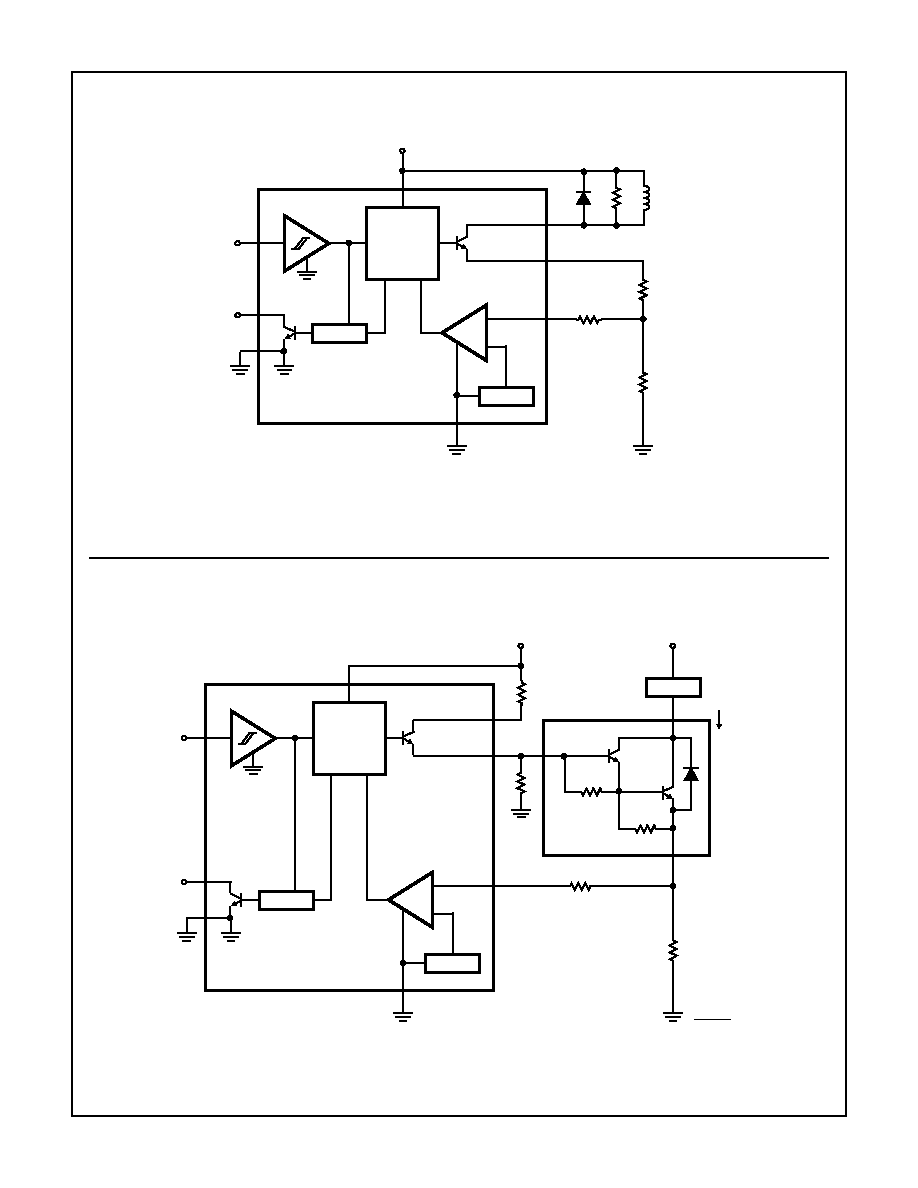
Block Diagram
FIGURE 1. TYPICAL APPLICATION AS A POWER SWITCH PRE-DRIVER SWITCH
CONTROL
LOGIC AND
CURRENT
LIMITER
CONTROL
IN
7
V
CC
8
Q2
D1
R4
RELAY OR
SOLENOID LOAD
-
+
LATCH
Q1
FLAG
OUT
SIGNAL
GROUND
1
4
335mV
3
POWER
GROUND
SENSE
IN
2
5
6
R2
DRIVE IN
DRIVE OUT
R3
SENSE
R1
CONTROL
LOGIC &
CURRENT
LIMITER
CONTROL
IN
7
V
CC
Q2
-
+
LATCH
Q1
FLAG
OUT
SIGNAL
GROUND
1
4
335mV
3
POWER
GROUND
SENSE
IN
DRIVE
V
CC1
LOAD
0.056
6A
SENSE LEVEL EQUALS
335mV
0.056
= 6A
8
2
5
6
DARLINGTON

10-42
Specifications CA3274
Absolute Maximum Ratings
Thermal Information
Operating Drive Supply, V
CC
. . . . . . . . . . . . . . . . . . . . . . . . . . . 16V
Maximum Output Current, I
O
. . . . . . . . . . . . . . . . . . . . . . . . . 200mA
Control, Sense Input. . . . . . . . . . . . . . . . . . . Gnd - 0.5V, V
CC
+ 0.5V
Signal, Power Differential Ground Voltage
. . . . . . . . . . . . . . . . . . . ±
1V
Thermal Resistance
JA
Plastic DIP Package 8 Lead . . . . . . . . . . . . . . . . . . . . . 130
o
C/W
Power Dissipation, P
D
Up to 70
o
C. . . . . . . . . . . . . . . . . . . . . . . . . . . . . . . . . . . . . 630mW
Above 70
o
C . . . . . . . . . . . . . . . . . . . . Derate linearly at 7.7mW/
o
C
Operating Temperature Range . . . . . . . . . . . . . . . . . -40
o
C to +85
o
C
Storage Temperature Range. . . . . . . . . . . . . . . . . . -55
o
C to +150
o
C
Lead Temperature (During Soldering)
At distance 1/16in. (1.59mm
±
0.79mm) from
case for 10s Max. . . . . . . . . . . . . . . . . . . . . . . . . . . . . . . . +265
o
C
CAUTION: Stresses above those listed in "Absolute Maximum Ratings" may cause permanent damage to the device. This is a stress only rating and operation
of the device at these or any other conditions above those indicated in the operational sections of this specification is not implied.
Electrical Specifications
At T
A
= -40
o
C to +85
o
C, Unless Otherwise Specified
PARAMETERS
SYMBOL
TEST CONDITIONS
MIN
TYP
MAX
UNITS
Power Supply Current: S1 = 2
I
CCH
Control = High (Output On)
-
-
25
mA
I
CCL
Control = Low (Output Off)
-
-
5
mA
Control Input: S1 = 3
V
THDH
Thd. Voltage, High
-
-
3.5
V
V
THDL
Thd. Voltage, Low
0.9
-
-
V
V
THDH
-V
THDL
Hysteresis
0.4
0.65
2.0
V
I
IL
Leakage, 0.0 to 5.5V
-20
-
+20
µ
A
Driver In, Out (Pin 6, 5): S1 = 3
V
SAT
Output Saturation Voltage, I
CC1
= 200mA,
V
CONTROL
= High
-
-
0.5
V
I
LEAK
Collector Output Leakage, V
CONTROL
=
Low
-
-
100
µ
A
Flag Output Low: S1 = 2
V
FSAT
V
SENSE
= High, I
FLAG
= 3mA
-
-
0.8
V
Flag Output High: S1 = 3
V
FLEAK
Output Leakage, V
CC
= V
FLAG
= 10V
-
-
10
µ
A
Prop. Delay: S1 = 1
t
ON
, t
OFF
Control In to Drive Out
-
5
-
µ
s
t
FLAG
Drive Off to Flag Off
-
10
-
µ
s
t
D
Flag Delay from Control In
150
-
600
µ
s
Sense Input Thd. Level: S1 = 1
V
SENTHD
310
335
360
mV
Power Supply Rejection Ratio
PSSR
50
-
-
dB
NOTES:
1. Refer to Figure 3 Test Diagram for electrical test connections.
2. Refer to Figure 2 Timing Diagram for logic switching and prop delay.
3. Unless otherwise specified: V
CC
= V
CC1
= V
CC2
= 7V to 10V;
V
SENSE
= "Low"; V
CONTROL
= "Low";
Control in levels are defined as "Low" equals 0.0V and "High" equals 5.0V.
10-43
CA3274
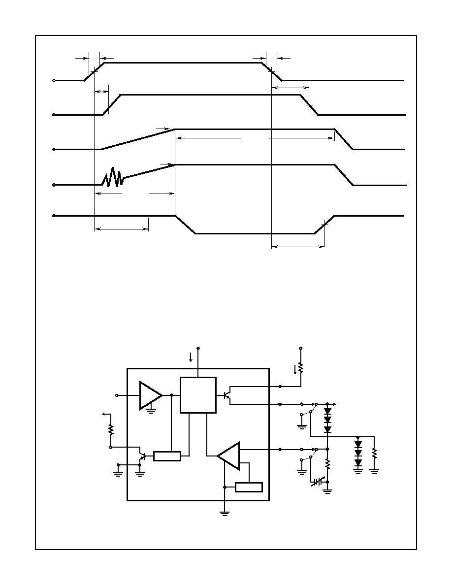
FIGURE 2. CA3274 TIMING DIAGRAM
FIGURE 3. CA3274 TEST CIRCUIT
CONTROL IN - PIN 7
DRIVE OUT- PIN 5
SENSE IN - PIN 2
FLAG OUT- PIN 1
3.35mV
SENSE
LEVEL
CURRENT
LIMITING
ON TIME
t
SENSE
OUTPUT
LOAD CURRENT
SYSTEM
NOISE
t
RISE
t
ON
DELAY
t
OFF
DELAY
t
FLAG
DELAY
(NOISE HOLD-OFF
DELAY)
t
D
(SEE NOTE)
NOTE: For V
CC
= 7V to 10V; t
D
(MAX) = 600
µ
S, if Control In = High,
Sense In = High; Pin 1, Flag Out can go low only if t
SENSE
t
D
t
FALL
CONTROL
LOGIC
IN V
CONTROL
7
Q2
-
+
LATCH
Q1
FLAG
OUT
SIGNAL
GROUND
1
4
335mV
3
POWER
GROUND
8
2
5
6 IN
POWER SUPPLY
+V
CC
I
CC
+V
CC2
10K
(ADJ. FOR 3mA
IN FLAG-OUT
V
SAT
TEST
OUT
DRIVER
OUTPUT LOAD
POWER SUPPLY
+V
CC1
51
IN
(ADJ. FOR 200mA
IN V
SAT
TEST)
S1
2.1V
1
3
(PSSROUT)
SENSE
IN
S1
1
3
2.1V
120
120
V
SENSE
10-44
All Intersil semiconductor products are manufactured, assembled and tested under ISO9000 quality systems certification.
Intersil products are sold by description only. Intersil Corporation reserves the right to make changes in circuit design and/or specifications at any time without
notice. Accordingly, the reader is cautioned to verify that data sheets are current before placing orders. Information furnished by Intersil is believed to be accurate
and reliable. However, no responsibility is assumed by Intersil or its subsidiaries for its use; nor for any infringements of patents or other rights of third parties which
may result from its use. No license is granted by implication or otherwise under any patent or patent rights of Intersil or its subsidiaries.
For information regarding Intersil Corporation and its products, see web site http://www.intersil.com
Sales Office Headquarters
NORTH AMERICA
Intersil Corporation
P. O. Box 883, Mail Stop 53-204
Melbourne, FL 32902
TEL: (407) 724-7000
FAX: (407) 724-7240
EUROPE
Intersil SA
Mercure Center
100, Rue de la Fusee
1130 Brussels, Belgium
TEL: (32) 2.724.2111
FAX: (32) 2.724.22.05
ASIA
Intersil (Taiwan) Ltd.
Taiwan Limited
7F-6, No. 101 Fu Hsing North Road
Taipei, Taiwan
Republic of China
TEL: (886) 2 2716 9310
FAX: (886) 2 2715 3029
CA3274
File Number