 | –≠–ª–µ–∫—Ç—Ä–æ–Ω–Ω—ã–π –∫–æ–º–ø–æ–Ω–µ–Ω—Ç: CA3277 | –°–∫–∞—á–∞—Ç—å:  PDF PDF  ZIP ZIP |
7-39
CAUTION: These devices are sensitive to electrostatic discharge; follow proper IC Handling Procedures.
407-727-9207
|
Copyright
©
Intersil Corporation 1999
CA3277
Dual 5V Regulator with Serial Data Buffer
Interface for Microcontroller Applications
Description
The CA3277 is a Dual 5V Voltage Regulator IC intended for micro-
processor and logic controller applications. It is supplied with fea-
tures that are commonly specified for sequentially controlled
shutdown and startup requirements of microcontrollers. Over-volt-
age shutdown, short circuit current limiting and thermal shutdown
features are provided for protection in the harsh environmental appli-
cations of industrial and automotive systems. The CA3277 functions
are complementary to the needs of microcontroller and memory cir-
cuits, providing for sustained memory with a 5V standby output.
The Ignition Comparator senses the voltage level at the IGN IN input
and provides a 5V logic switched output (supply sourced from
OUT1). The Ignition Output, IGN OUT can be used to signal a sys-
tem microcontroller which can respond with a logic switched output
to the CA3277 ENABLE input control for OUT2. The OUT1 +5V
Standby Supply of the regulator is normally used as a power supply
for microcontroller/memory circuits to preserve stored data when in
the standby mode.To allow for maximum heat transfer from the chip,
the four center leads are directly connected to the die mounting pad.
Refer to AN9302 for further information on CA3277 circuit Applica-
tions.
Ordering Information
PART NUMBER
TEMPERATURE RANGE
PACKAGE
CA3277E
-40
o
C to +85
o
C
16 Lead Plastic DIP
Features
∑ Dual 5V Regulator
- V
OUT
1 at 5V 100mA - Standby
- V
OUT
2 at 5V 100mA - Enabled
- Regulation Range 6V to 18V
- Bandgap Voltage References
∑ Low Quiescent Idle Current, 500
µ
A Typ.
∑ Over-Voltage Shutdown Protection, 20.5V Typ.
∑ Reverse Battery Protection, -26V Max.
∑ Thermal Shutdown Protection
∑ Short Circuit Current Limiting
∑ Low Input P.S. Flag and Delayed Reset Control
∑ Low Voltage Shutdown Control, Ouput1
∑ Ignition Comparator Logic Level Control
∑ Data Comparator and 100X Current Mult. Used
as Input/Output Buffers for Remote Serial Data
Communication
Applications
∑ Automotive 5V Regulators and Data Buffers
∑ Industrial Controller Remote System
∑ Microcontroller and Memory Power Supply
∑ Radio, TV, CATV, Consumer Applications
File Number
2792.4
April 1994
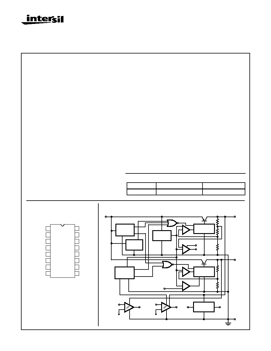
Pinout
CA3277 (PDIP)
TOP VIEW
14
15
16
9
13
12
11
10
1
2
3
4
5
7
6
8
IGN
ENABLE
GND
GND
IGN OUT
CUR IN
CUR OUT
OUT2
BATT
OUT1
DATA IN
GND
GND
DATA OUT
RESET
CRST
Functional Block Diagram
4, 5 AND
12, 13
OUT1 REG.
DR. CNTRL
BANDGAP
VOLTAGE
REF
2
RESET
CRST
8
7
BATT
1
OVER-
SHTDWN
15
OVER-
SHTDWN
ENABLE 14
CURRENT
MULTIPLIER
IGN
11
OUT
10
CUR
OUT
9
16
IGN IN
3
DATA IN
6
DATA
OUT
GND
-
+
(OUTPUT2)
TEMP
OUT2 REG.
DR. CNTRL
OUT1
OUT2
LOW
VOLTAGE
SHTDWN
VOLTAGE
V
BATT
-2.9V
6V
1.2V
+5V
(STANDBY)
+5V
(ENABLE)
CUR
IN
-
+
IN
-
+
-
+
-
+
-
+

7-40
Specifications CA3277
Absolute Maximum Ratings
Thermal Information
Max. BATT, IGN IN Input Voltage (Note1) . . . . . . . . . . . . . . .
±
26V
Max. Operating Voltage; BATT, IGN IN . . . . . . . V
BATT(SD)
(~20.5V)
Max. Positive Voltages: (For Negative Voltages, Note 2)
ENABLE Input. . . . . . . . . . . . . . . . . . . . . . . . . . . . . . . . . . . . V
BATT
DATA IN Input . . . . . . . . . . . . . . . . . . . . . . . . . . . . . . . . . . . . V
BATT
CUR OUT, Output . . . . . . . . . . . . . . . . . . . . . . . . . . . . . . . . . V
BATT
RESET, Output . . . . . . . . . . . . . . . . . . . . . . . . . . . . . . . . . . . V
BATT
Max. Operating Load Current, OUT1 . . . . . . . . . . . . . . . . . . . 100mA
Max. Operating Load Current, OUT2 . . . . . . . . . . . . . . . . . . . 100mA
Max. Current Mult. Load Currents:
Min. Load Resistance, CUR OUT . . 225
to BATT (75mA max)
Min. Load Resistance, CUR IN . . . . . . 1K
to GND (-5mA max)
Max. Load Current OUT1, OUT2 (Short Duration) . . . Self-Limiting
Max. Plus/Minus Load Currents: (Note 3)
IGN OUT Output . . . . . . . . . . . . . . . . . . . . . . . . . . . . .Self-Limiting
DATA OUT Output . . . . . . . . . . . . . . . . . . . . . . . . . . .Self-Limiting
RESET Output . . . . . . . . . . . . . . . . . . . . . . . . . . . . . .Self-Limiting
Thermal Resistance
JA
JL
Plastic DIP Package . . . . . . . . . . . . . . . .
60
o
C/W
12
o
C/W
(Temp. meas. on center lead next to case)
Power Dissipation, P
D
(Note 4):
Up to +60
o
C (Free Air). . . . . . . . . . . . . . . . . . . . . . . . . . . . . . 1.5W
Above +60
o
C: . . . . . . . . . . . . . . . . Derate Linearly at 16.6mW/
o
C
Up to +85
o
C w/heat sink (PC Board): . . . . . . . . . . . . . . . . . 1.6 W
Operating Temperature Range . . . . . . . . . . . . . . . . . -40
o
C to +85
o
C
Storage Temperature Range. . . . . . . . . . . . . . . . . . -55
o
C to +150
o
C
Max. Junction Temperature. . . . . . . . . . . . . . . . . . . . . . . . . . +150
o
C
Lead Temperature (During Solder) . . . . . . . . . . . . . . . . . . . . +265
o
C
1/16
±
1/32" from case, 10s max
CAUTION: Stresses above those listed in "Absolute Maximum Ratings" may cause permanent damage to the device. This is a stress only rating and operation
of the device at these or any other conditions above those indicated in the operational sections of this specification is not implied.
Electrical Specifications
T
A
= -40
o
C to +85
o
C, V
BATT
= 13.5V, ENABLE ON (V
EN
= 3.5V), IGN IN connected to BATT, OUT1 and
OUT2 bypassed with 20
µ
F to GND, DATA IN connected through 250
to BATT, LOADS: OUT1 = 50mA,
OUT2 = 80mA; Unless Otherwise Specified (Refer to Figure 4 Test Circuit)
PARAMETERS
SYMBOL
CONDITIONS
MIN
TYP
MAX
UNITS
REGULATOR OUTPUT1
Output Voltage
V
OUT1
V
BATT
= 9V to 16V
4.75
5
5.25
V
Dropout Voltage (Note 5)
V
DO1
V
BATT
= 4.75V
4.15
4.6
-
V
Line Reg
V
BATT
= 6.2V to 16V
-
9
40
mV
Load Reg
I
LOAD
= 0.5mA to 50mA
-
30
60
mV
Current Limiting
-
170
250
mA
Low Voltage Shutdown
Ramp V
BATT
Down Until OUT1 drops (PNP Driv-
er Cutoff)
-
3.5
-
V
REGULATOR OUTPUT2
Output Voltage
V
OUT2
V
BATT
= 9V to 16V
4.75
5
5.25
V
Dropout Voltage (Note 5)
V
DO2
V
BATT
= 5.6V
4.6
5
-
V
Line Reg
V
BATT
= 6.2V to 16V
-
7.5
40
mV
Load Reg
I
LOAD
= 0.5mA to 80mA
-
35
60
mV
Current Limiting
-
190
250
mA
ENABLE Input Current
I
EN
V
EN
= 5V
-
50
150
µ
A
ENABLE Input Sw. Thd.
V
EN(THD)
Ramp ENABLE Input Up Until OUT2 is
Switched ON
-
1.2
-
V
CURRENT MULTIPLIER
Current Mult. Gain, (I
COUT
/I
CIN
)
I
CIN
= -200
µ
A
80
100
-
Gain
Ratio
Current Mult. Output Sat.
V
COUT(SAT)
I
CIN
= -200
µ
A, CUR OUT Load = 1K
to V
BATT
-
0.3
1
V
Current Mult., Max. Drive Cur.
I
COUT(MAX)
I
CIN
= -700
µ
A
35
50
-
mA
RESET
Reset, (RST) Threshold
Ramp V
BATT
Down, Measure V
BATT
when
RESET (V
RST
) goes low
3.8
4.2
4.5
V
Reset Delay Time (Note 6)
t
RST
CRST Cap. = 0.47
µ
F, V
BATT
= 6.8V
RESET Load = 5K
to OUT1
50
150
250
ms
RESET Out High
V
OH(RST)
47K
to OUT1
4
-
-
V
RESET Low
V
OL(RST)
V
BATT
= 3.75V, RST 47K
to OUT1
-
-
0.2
V
RESET Output Sink Current
I
OL
CRST to GND, V
BATT
= 6.8V
-
8
-
mA

7-41
Specifications CA3277
DATA COMPARATOR
Data Comp Thd
V
BATT
- 3.6
V
BATT
-2.9
V
BATT
-2.2
V
Data Comp Hysteresis
-
200
-
mV
DATA OUT Low
V
OL
V
BATT
= 16V, V
DATA IN
= (V
BATT
-5V)
-
-
0.15
V
DATA OUT High
V
OH
V
BATT
= 16V, V
DATA IN
= 16V
V
OUT1
-0.15
-
5.25
V
DATA OUT Low Sink Current
I
OL
V
DATA IN
Low
-
1
-
mA
DATA OUT High Source Current
I
OH
V
DATA IN
High
-
-50
-
µ
A
IGNITION COMPARATOR
Ign Comp Thd
5.5
6
6.5
V
Ign Comp Hysteresis
-
200
-
mV
IGN OUT Low
V
OL
-
-
0.15
V
IGN OUT High
V
OH
4.6
5.25
V
IGN OUT Low Sink Current
I
OL
V
IGN IN
Low
-
1
-
mA
IGN OUT High Source Current
I
OH
V
IGN IN
High
-
-70
-
µ
A
OTHER PARAMETERS
Idle Current
I
Q
V
BATT
= 12.6V, No Loads, V
EN
= V
IGN IN
= 0V
-
500
800
µ
A
Over-Voltage Shutdown
V
BATT(OVSD)
Ramp V
BATT
Up Until OUT1 and OUT2 Shut-
down
19
20.5
23
V
Thermal Shutdown
T
J
-
150
-
o
C
Ripple Rejection
1V
PP
at 3kHz on BATT INPUT, Measure AC
Ripple on OUT1, OUT2
45
55
-
dB
NOTES:
1. For negative voltages on the BATT and IGN IN inputs, current drain is primarily reverse junction leakage, except when DATA IN, CUR
OUT, ENABLE and RESET are directly connected to BATT. (Note 2)
2. For negative voltage DATA IN, CUR OUT, ENABLE and RESET interface to NPN or equivalent on-chip structures; providing a forward
junction for current conduction into the IC. Negative current must be limited by the impedance of the external connection. This is also the
case where these terminals are interconnected to BATT, Normal application does not require the BATT connection, except for DATA IN
where a series diode for reverse current blocking may be used. (see Description text information)
3. Refer to the Electrical Characteristic TABLE for all Self-Limiting values.
4. Dissipation, approximately equals: P
D
[(V
IN
I
IN
) + (V
CUR OUT
I
CUR OUT
) - 5(I
OUT1
+I
OUT2
)], where I
IN
V
IN
is IGN IN and BATT input dissi-
pation and V
OUT1
~
V
OUT2
~
5V. This assumes neglibible dissipation for the Ignition Comp., Reset and Data Comp. Outputs.
5. Dropout Voltage is V
DO1
= (V
BATT
- V
OUT1
) for REG. OUT1 and V
DO2
= (V
BATT
- V
OUT2
) for REG. OUT2
6. Reset Delay Time, t
RST
is the time period that the RESET (Pin 8) is low following the discharge of the CRST capacitor to ground. For test
evaluation, the CRST pin may be discharged repetitively with a transistor switch. The RESET pin switches from low to high when the
CRST pin is charged to approximately 3V. Normal ATE testing measures the source charging current. which is typically 10
µ
A. For any
other value of Capacitor the charge time, t for reset is determined as follows: t
~
308C, where C is in
µ
F and t is in milliseconds.
(i.e. C = 0.47
µ
F, t = 141ms)
Electrical Specifications
T
A
= -40
o
C to +85
o
C, V
BATT
= 13.5V, ENABLE ON (V
EN
= 3.5V), IGN IN connected to BATT, OUT1 and
OUT2 bypassed with 20
µ
F to GND, DATA IN connected through 250
to BATT, LOADS: OUT1 = 50mA,
OUT2 = 80mA; Unless Otherwise Specified (Refer to Figure 4 Test Circuit) (Continued)
PARAMETERS
SYMBOL
CONDITIONS
MIN
TYP
MAX
UNITS
7-42
CA3277
Applications
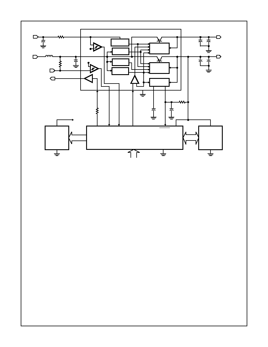
Other functions of the CA3277 include a Data Comparator
and Current Multiplier for use as interface buffers to transfer
serial data at higher level logic to and from a remote host
microcontroller. The OUT1 5V Standby Supply provides
power to the local microcontroller which interfaces to the
CA3277 interface buffers at a 5V logic level. As shown in
Figure 1, the DATA IN input of the Data Comparator receives
serial data referenced to the BATT voltage level. The output
of the Data Comparator is 5V CMOS compatible logic and is
connected to the RDI (remote data input) terminal of the
microcontroller. The TDO (data out) output of the microcon-
troller is connected to the Current Multiplier input of the
CA3277.
Current Multiplier - The Current Multiplier, with internal cir-
cuitry shown in Figure 2, receives data from the
microcontroller in the form of an open drain or gate switched
output driving a 22K
resistor load in series to the Current
Input at pin 10 (CUR IN). The input stage of the Current Mul-
tiplier is a current mirror amplifier which is internally
connected to the 5V regulated OUT1 voltage source. The
output stage of the Current Multiplier is a current mirror
amplifier referenced to GND and has an open collector
Current Output at pin 9 (CUR OUT), with a minimum drive
capability of 35mA. The Current Multiplier output load is
normally connected via resistive loading to the BATT voltage
supply level. As such, the microcontroller transmits data out
(TDO output) to the input of the CA3277 Current Multiplier
which amplifies and translates the signal back to the voltage
reference level of the BATT power supply input. When
driving a similar remote CA3277, the voltage drop from the
BATT input line switches the Data Comparator which
provides serial data to the RDI input of the remote microcon-
troller. The nominal current gain of the Current Multiplier is
100X.
The application use of the Current Multiplier is not limited to
digital serial data transfer. The Current Multiplier is an
independent function and is open to use for other purposes,
including linear signal amplification, sensor output amplifica-
tion and current controlled threshold switching. The current
output terminal, CUR OUT may be externally load-
connected to OUT1, OUT2, BATT or any other power supply
level up to the maximum ratings given for the BATT input
terminal. It is important to note that some applied uses of the
Current Multiplier may contribute significant on-chip power
dissipation. A nominal current mirror input drive of 200
µ
A will
provide sufficient drive to switch a 250
resistor load at the
input of the data comparator. As such, the quiescent OFF
condition of the Data comparator should be in the High state.
FIGURE 1. TYPICAL APPLICATION CIRCUIT OF THE CA3277 DUAL 5V REGULATOR WITH MICROCONTROLLER AND SERIAL
DATA BUFFER INTERFACE TO A REMOTE HOST
IGN IN
BATT
CUR OUT
CUR
IN
(OUT2)
EN
DATA
OUT
IGN
OUT
CRST
RESET
OUT2
GND
OUT1
47K
0.01
µ
F
0.47
µ
F
22k
100
µ
F
0.1
µ
F
TO
+5V
DISPLAY OR
CONTROL
OUTPUT
BUS
5V MICROCONTROLLER
TDO
CONTROL
RDI SENSE
IN
RESET VDD
VSS
+5V
CMOS
MEMORY
DATA IN
UNREG
IGN IN
220
0.1
µ
F
330
150
µ
H
+5V ENABLE
+5V
C2
SUPPLY IN
(V
BATT
-2.9V)
6V
ERROR AMP
CONTROL
FB
FB
STANDBY
OUTPUT
SWITCHED
OUTPUT
LOW VOLT
RESET
SHTDWN
BANDGAP
OUT2
LOW VOLT
OVR-VOLT
SHTDWN
IGNITION
COMP
DATA
COMP
OUT
CURRENT
AMP
I
OVR-TEMP
SHTDWN
REF
OUT2
ENABLE
AND OUTPUT
ERROR AMP
CONTROL
AND OUTPUT
R1
C1
L1
R4
C3
C4
R5
C7
C8
CA3277
200
µ
F
22
µ
F
0.1
µ
F
C5
C6
NOTE:
DATA IN and CUR OUT are remote/host Serial Data Communication Buffers. Typical Remote Source
Impedance for DATA IN is 1k
. Typical Remote Load for CUR OUT is 250
.

7-43
CA3277
FIGURE 2. CURRENT MULTIPLIER DRIVING A REMOTE
CA3277 DATA COMPARATOR
Data Comparator - The Data Comparator provides a means
of translating serial data from a high to low voltage. The
DATA IN terminal of the Data Comparator is biased to
receive signal input that is source referenced to the BATT
supply voltage level. In normal use the signal input would be
supplied from a remote Current Multiplier having a resistor
load tied to the BATT voltage supply. The DATA OUT output
from the Data Comparator is CMOS compatible 5V non-
inverting logic data referenced to GND. The switching
threshold at the DATA IN input is bias stabilized by the band-
gap voltage and is typically at (V
BATT
- 2.9V). The Data
Comparator is in a high state when DATA IN input is at the
BATT voltage level and is in a low state when DATA IN is at
(V
BATT
- 5V). The output stage of the Data Comparator is
internally supply biased from the Switched 5V Regulator
output to provide a high state of 5V and a low state of 0V
(GND). The DATA OUT terminal can typically sink 1.2mA in a
low state or source 50
µ
A in a high state.
In system applications the Data Comparator is used to
translate remote data at high voltage down to 5V logic levels.
The Current Multiplier is used to reverse the process by
translating 5V logic data back to the BATT voltage level
when sending data back to the remote system. The Data
Comparator and Current Multiplier are level matched for
remote communication between microcontroller systems
using the common BATT power supply voltage of the
CA3277. The current driven serial data from the Current
Multiplier is sent to a remote system by translating the signal
up to the BATT voltage level, or an external power supply
level that is compatible with the remote device. The Data
Comparator of the remote system receives the data,
interfaces to its microcontroller and responds with signal
drive from its Current Multiplier to translate the signal back to
the host. For best noise immunity the transmission in each
direction should be over a twisted pair or shielded line. As
such, two microcontrollers, each with the interface protection
of a CA3277, can provide intelligent master/slave system
communications under adverse environmental conditions.
510
250
CA3277
REMOTE
SYSTEM
+
-
DATA
COMP.
BATT
DI
CA3277
INTERNALLY
CONNECTED
TO OUT1 (+5V)
Q100
Q99
5X
GAIN
I
CIN
Q103
Q102
C3
10pF
Q101
CUR
IN
10
20X
GAIN
9
CUR
OUT
GND
4, 5 AND
12, 13
Ignition Comparator - While the Ignition Comparator is pro-
vided as an essential part of the start-up control in automo-
tive systems, this circuit function may be used as an
independent switching comparator. It is important to note
that the thermal shutdown feature on the chip is dis-
abled when the IGN IN input is low. Disabling of the on-
chip thermal protection is done to satisfy the requirement of
low idle current when the system is in a standby condition.
The non-inverting IGN IN input has a switching threshold of
typically 6V with 200mV of hysteresis and is switched with
logic levels reference to GND as the low state and BATT as
the high state. The IGN OUT output is 5V CMOS compatible
logic, equivalent to the Data Comparator output stage, but is
internally supply biased from the Standby 5V Regulator. As
such, the high state is level referenced to OUT1. The IGN
OUT output terminal can typically sink 1.2mA in a low state
or source 70
µ
A in a high state.
Enable - A CMOS or TTL high at the ENABLE input
switches the regulated 5V/Switched Output ON at OUT2.
The ENABLE input has an internal pull-down of typically
50
µ
A to ensure that OUT2 is OFF when the ENABLE input
is not connected. The input threshold level for switching is
the bandgap voltage reference of 1.2V. When the ENABLE
input is low, all drive current to the output pass transistor is
cutoff and OUT2 voltage drops to ground level. The ENABLE
input is normally switched from the interfacing microcontrol-
ler but may be activated from a remote source.
Reset - The purpose of the Low Voltage Reset function is to
flag a low voltage condition at OUT1. When the RESET out-
put, pin 8 switches low, the voltage level at OUT1 has
dropped below the regulation level. The CRST and RESET
are high when OUT1 is at 5V. When OUT1 drops to less than
4.2V (typical), the CRST Capacitor at pin 7 is internally
discharged, causing the RESET pin to change from a high to
a low state, outputting a negative going pulse. The RESET
output is an NPN open collector driver requiring an external
load resistor, normally connected to OUT1. The RESET
output flag may be sent to a microcontroller to initiate a
power-down sequence. For any condition that causes OUT1
to drop below the reset threshold, such as undesired
transients, the RESET output is switched low for a delay
period, t
RST
determined by the value of the external
capacitor, C
RST
at CRST terminal. For a value of 0.47
µ
F the
delay period is typically 141ms. This correlates to approxi-
mately
10µ
A of charging current sourced from the CRST
terminal to charge C
RST
.
Regulation - The regulated output stages of the CA3277
have similar circuits, each having an error amplifier to
compare the output voltage to the bandgap reference
voltage. The circuit of the 5V/Switched regulator is shown in
Figure 3. By feedback, the output voltage is differentially
compared to the bandgap reference voltage. The error signal
is then amplified to drive a PNP pass transistor and maintain
a stable 5V output with both line and load regulation over the
full operating temperature range. Except for the ENABLE
control of OUT2, the OUT1 drive circuit is similar to the
OUT2 circuit.