 | –≠–ª–µ–∫—Ç—Ä–æ–Ω–Ω—ã–π –∫–æ–º–ø–æ–Ω–µ–Ω—Ç: CA3290AS | –°–∫–∞—á–∞—Ç—å:  PDF PDF  ZIP ZIP |

1
CA3290, CA3290A
BiMOS Dual Voltage Comparators
with MOSFET Input, Bipolar Output
The CA3290A and CA3290 types consist of a dual voltage
comparator on a single monolithic chip. The common mode
input voltage range includes ground even when operated
from a single supply. The low supply current drain makes
these comparators suitable for battery operation; their
extremely low input currents allow their use in applications
that employ sensors with extremely high source
impedances. Package options are shown in the table below.
Pinout
CA3290/A (PDIP)
TOP VIEW
Features
∑ MOSFET Input Stage
- Very High Input Impedance (Z
IN
) . . . . . . . . 1.7T
(Typ)
- Very Low Input Current at V+ = 5V . . . . . . . 3.5pA (Typ)
- Wide Common Mode Input Voltage Range (V
ICR
) Can Be
Swung 1.5V (Typ) Below Negative Supply Voltage Rail
- Virtually Eliminates Errors Due to Flow of Input Currents
∑ Output Voltage Compatible with TTL, DTL, ECL, MOS,
and CMOS Logic Systems in Most Applications
Applications
∑ High Source Impedance Voltage Comparators
∑ Long Time Delay Circuits
∑ Square Wave Generators
∑ A/D Converters
∑ Window Comparators
Schematic Diagram
(ONLY ONE IS SHOWN)
OUTPUT (A
1
)
INV. INPUT (A
1
)
NON-INV. INPUT (A
1
)
V-
1
2
3
4
8
7
6
5
V+
OUTPUT (A
2
)
INV. INPUT (A
2
)
NON-INV. INPUT (A
2
)
-
+
-
+
A
1
A
2
Ordering Information
PART
NUMBER
TEMP
RANGE (
o
C)
PACKAGE
PKG. NO.
CA3290AE
-55 to 125
8 Ld PDIP
E8.3
CA3290E
-55 to 125
8 Ld PDIP
E8.3
D
1
+V
I
-V
I
D
2
I
1
Q
9
I
2
Q
10
I
3
Q
11
I
4
Q
12
Q
2
Q
3
Q
5
Q
6
D
3
D
4
Q
4
COMPARATOR NO. 1
Q
7
V
O
Q
1
BIASING CIRCUIT
FOR CURRENT
SOURCES
TO
COMP.
NO. 2
R
1
100k
Q
8
Q
15
Q
13
Q
14
Q
16
Q
17
Q
18
R
2
1k
R
3
5k
C
1
5pF
V-
V+
50
µ
A
100
µ
A
50
µ
A
100
µ
A
Data Sheet
September 1998
File Number
1049.3
CAUTION: These devices are sensitive to electrostatic discharge; follow proper IC Handling Procedures.
1-888-INTERSIL or 321-724-7143
|
Copyright
©
Intersil Corporation 1999
2
Absolute Maximum Ratings
Thermal Information
Supply Voltage
Single Supply . . . . . . . . . . . . . . . . . . . . . . . . . . . . . . . . . . . . +36V
Dual Supply
. . . . . . . . . . . . . . . . . . . . . . . . . . . . . . . . . . . . . . . . . . ±
18V
Differential Input Voltage . . . . . . . . . . . . . . . . 36V or [(V+ - V-) +5V]
(whichever is less)
DC Input Voltage . . . . . . . . . . . . . . . . . . . . . . . . . . V+ +5V to V- -5V
Output to V- Short Circuit Duration (Note 1) . . . . . . . . . . Continuous
Input Current . . . . . . . . . . . . . . . . . . . . . . . . . . . . . . . . . . . . . . . 1mA
Operating Conditions
Temperature Range . . . . . . . . . . . . . . . . . . . . . . . . . . . -55 to 125
o
C
Thermal Resistance (Typical, Note 2)
JA
(
o
C/W)
JC
(
o
C/W)
PDIP Package . . . . . . . . . . . . . . . . . . .
120
N/A
Maximum Junction Temperature (Plastic Package) . . . . . . . . .150
o
C
Maximum Storage Temperature Range . . . . . . . . . . -65
o
C to 150
o
C
Maximum Lead Temperature (Soldering 10s) . . . . . . . . . . . . 300
o
C
CAUTION: Stresses above those listed in "Absolute Maximum Ratings" may cause permanent damage to the device. This is a stress only rating and operation of the
device at these or any other conditions above those indicated in the operational sections of this specification is not implied.
NOTES:
1. Short circuits from the output to V+ can cause excessive heating and eventual destruction of the device.
2.
JA
is measured with the component mounted on an evaluation PC board in free air.
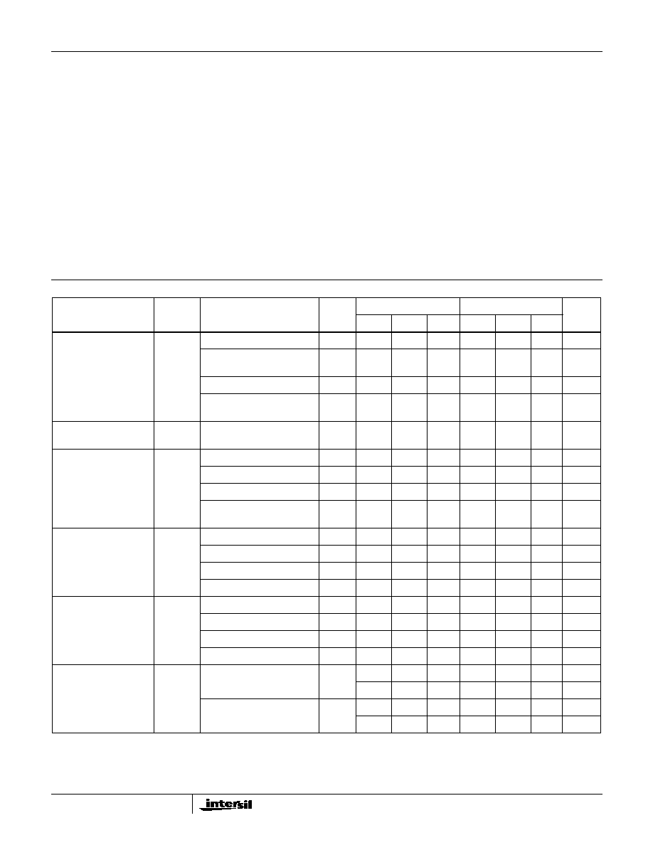
Electrical Specifications
V- = 0V, Unless Otherwise Specified
PARAMETER
SYMBOL
TEST CONDITIONS
TEMP
(
o
C)
CA3290A
CA3290
UNITS
MIN
TYP
MAX
MIN
TYP
MAX
Input Offset Voltage
V
IO
V
CM
= V
O
= 1.4V, V+ = 5V
Full
-
4.5
-
-
8.5
-
mV
V
CM
= V
O
= 0V, V+ =
+
15V,
V- = -15V
Full
-
8.5
-
-
8.5
-
mV
V
CM
= V
O
= 1.4V, V+ = 5V
25
-
4.0
10
-
7.5
20
mV
V
CM
= V
O
= 0V, V+ = +15V,
V- = -15V
25
-
4.0
10
-
7.5
20
mV
Temperature Coefficient
of Input Offset Voltage
V
IO
/
T
-
8
-
-
8
-
µ
V/
o
C
Input Offset Current
I
IO
V
CM
= 1.4V, V+ = 5V
Full
-
2
28
-
2
32
nA
V
CM
= 0V, V+ = +15V, V- = -15V
Full
-
7
28
-
7
32
nA
V
CM
= 1.4V, V+ = 5V
25
-
2
25
-
2
30
pA
V
CM
= 0V,
V+ = +15V, V- = -15V
25
-
7
25
-
7
30
pA
Input Current
I
I
V
CM
= 1.4V, V+ = 5V
125
-
2.8
45
-
2.8
55
nA
V
CM
= 0V, V+ = +15V, V- = -15V
125
-
13
45
-
13
55
nA
V
CM
= 1.4V, V+ = 5V
25
-
3.5
40
-
3.5
50
pA
V
CM
= 0V, V+ = +15V, V- = -15V
25
-
12
40
-
12
50
pA
Supply Current
I+
R
L
=
, V+ = 5V
-55
-
0.85
1.0
-
0.85
1.6
mA
R
L
=
, V+ = 30V
-55
-
1.62
3.0
-
1.62
3.5
mA
R
L
=
, V+ = 5V
25
-
0.8
1.4
-
0.8
1.4
mA
R
L
=
, V+ = 30V
25
-
1.35
3.0
-
1.35
3.0
mA
Voltage Gain
A
OL
R
L
= 15k
, V+ =
+
15V,
V- = -15V
Full
-
150
-
-
150
-
V/mV
-
103
-
-
103
-
dB
R
L
= 15k
, V+ = +15V,
V- = -15V
25
25
800
-
25
800
-
V/mV
88
118
-
88
118
-
dB
CA3290, CA3290A

3
Saturation Voltage
V
SAT
I
SINK
= 4mA, V+ = 5V,
+V
I
= 0V, -V
I
= 1V
125
-
0.22
0.7
-
0.22
0.7
V
I
SINK
= 4mA, V+ = 5V,
+V
I
= 0V, -V
I
= 1V
-55
-
0.1
-
-
0.1
-
V
I
SINK
= 4mA, V+ = 5V,
+V
I
= 0V, -V
I
= 1V
25
-
0.12
0.4
-
0.12
0.4
V
Output Leakage Current
I
OL
V+ = 15V
Full
-
65
-
-
65
-
nA
V+ = 36V
Full
-
130
1k
-
130
1k
nA
V+ = 15V
25
-
100
-
-
100
-
pA
V+ = 36V
25
-
500
-
-
500
-
pA
Common Mode Input
Voltage Range
V
ICR
V
O
= 1.4V, V+ = 5V
25
V+ -3.5
V-
V+ -3.1
V- -1.5
-
V+ -3.5
V-
V+ -3.1
V- -1.5
-
V
V
O
= 0V, V+ = +15V, V- = -15V
25
V+ -3.8
V-
V+ -3.4
V- -1.6
-
V+ -3.8
V-
V+ -3.4
V- -1.6
-
V
Common Mode
Rejection Ratio
CMRR
V+ = +15V, V- = -15V
25
-
44
562
-
44
562
µ
V/V
V+ = 5V
25
-
100
562
-
100
562
µ
V/V
Power Supply Rejection
Ratio
PSRR
V+ = +15V, V- = -15V
25
-
15
316
-
15
316
µ
V/V
Output Sink Current
V
O
= 1.4V, V+ = 5V
25
6
30
-
6
30
-
mA
Response Time Rising
Edge
t
r
R
L
= 5.1k
, V+ = 15V
25
-
1.2
-
-
1.2
-
µ
s
Response Time Falling
Edge
t
f
R
L
= 5.1k
, V+ = 15V
25
-
200
-
-
200
-
ns
Large Signal Response
Time
R
L
= 5.1k
, V+ = 15V
25
-
500
-
-
500
-
ns
R
L
= 5.1k
, V+ = 5V
25
-
400
-
-
400
-
ns
Electrical Specifications
V- = 0V, Unless Otherwise Specified (Continued)
PARAMETER
SYMBOL
TEST CONDITIONS
TEMP
(
o
C)
CA3290A
CA3290
UNITS
MIN
TYP
MAX
MIN
TYP
MAX
Test Circuits and Waveforms
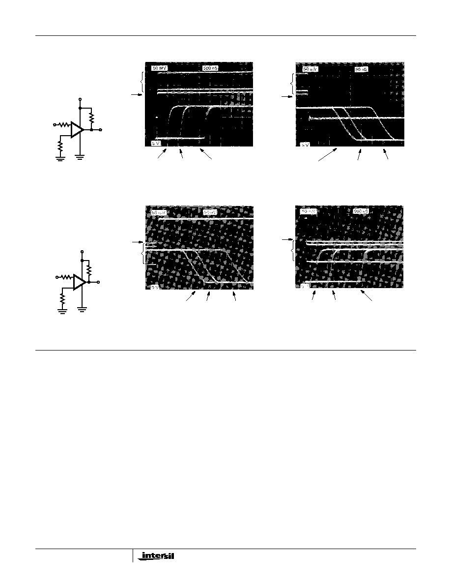
FIGURE 1. PARASITIC OSCILLATIONS TEST CIRCUIT AND WAVEFORMS
+
-
+15V
-15V
+15V
TO 10X
SCOPE
PROBE
1K
1K
V
IN
C
C
= 2pF
WITH C
C
Top Trace
4.5mV/Div. = V
IN
Bottom Trace = 10V/Div. = V
OUT
Time Scale = 5
µ
s/Div.
WITHOUT C
C
Top Trace
4.5mV/Div.
Bottom Trace = 10V/Div.
Time Scale = 5
µ
s/Div.
CA3290, CA3290A
4
Circuit Description
The Basic Comparator
Figure 4 shows the basic circuit diagram for one of the two
comparators in the CA3290. It is generically similar to the
industry type "139" comparators, with PMOS transistors
replacing PNP transistors as input stage elements. Transistors
Q
1
through Q
4
comprise the differential input stage, with Q
5
and Q
6
serving as a mirror connected active load and
differential-to-single-ended converter. The differential input at
Q
1
and Q
4
is amplified so as to toggle Q
6
in accordance with
the input signal polarity. For example, if +V
IN
is greater than
-V
IN
, Q
1
, Q
2
, and current mirror transistors Q
5
and Q
6
will be
turned off; Transistors Q
3
, Q
4
, and Q
7
will be turned on,
causing Q
8
to be turned off. The output is pulled positive
when a load resistor is connected between the output and V+.
In essence, Q
1
and Q
4
function as source followers to drive
Q
2
and Q
3
, respectively, with zener diodes D
1
through D
4
providing gate oxide protection against input voltage
transients (e.g., static electricity). The current flow in Q
1
and
Q
4
is established at approximately 50
µ
A by constant current
sources I
1
and I
3
, respectively. Since Q
1
and Q
4
are
operated with a constant current load, their gate-to-source
voltage drops will be effectively constant as long as the input
voltages are within the common-mode range.
As a result, the input offset voltage (V
GS(Q1)
+ V
BE(Q2)
-
V
BE(Q3)
- V
GS(Q4)
) will not be degraded when a large
differential DC voltage is applied to the device for extended
periods of time at high temperatures.
Additional voltage gain following the first stage is provided by
transistors Q
7
and Q
8
. The collector of Q
8
is open, offering
the user a wide variety of options in applications. An
additional discrete transistor can be added if it becomes
necessary to boost the output sink current capability.
The detailed schematic diagram for one comparator and the
common current source biasing is shown on the front page.
PMOS transistors Q
9
through Q
12
are the current source
elements identified in Figure 4 as I
1
through I
4
, respectively.
FIGURE 2. NON-INVERTING COMPARATOR RESPONSE TIME TEST CIRCUIT AND WAVEFORMS
FIGURE 3. INVERTING COMPARATOR RESPONSE TIME TEST CIRCUIT AND WAVEFORMS
Test Circuits and Waveforms
INPUT
OVERDRIVE
GND
100mV
OVERDRIVE
20mV
OVERDRIVE
5mV
OVERDRIVE
INPUT
OVERDRIVE
GND
100mV
OVERDRIVE
20mV
OVERDRIVE
5mV
OVERDRIVE
+15V
1K
1K
INPUT
5.1K
OUTPUT
+
-
INPUT
OVERDRIVE
GND
100mV
OVERDRIVE
20mV
OVERDRIVE
5mV
OVERDRIVE
INPUT
OVERDRIVE
GND
100mV
OVERDRIVE
20mV
OVERDRIVE
5mV
OVERDRIVE
+15V
1K
1K
INPUT
5.1K
OUTPUT
+
-
CA3290, CA3290A

5
Their gate source potentials (V
GS
) are supplied by a common
bus from the biasing circuit shown in the right hand portion of
the Schematic Diagram. The currents supplied by Q
10
and
Q
12
are twice those supplied by Q
9
and Q
11
. The transistor
geometries are appropriately scaled to provide the requisite
currents with common V
GS
applied to Q
9
through Q
12
.
Operating Considerations
Input Circuit
The use of MOS transistors in the input stage of the CA3290
series circuits provides the user with the following features
for comparator applications:
1. Ultra high input impedance (
1.7T
);
2. The availability of common mode rejection for input signals
at potentials below that of the negative power supply rail;
3. Retention of the in phase relationship of the input and out-
put signals for input signals below the negative rail.
Although the CA3290 employs rugged bipolar (zener) diodes
for protection of the input circuit, the input terminal currents
should not exceed 1mA. Appropriate series connected
limiting resistors should be used in circuits where greater
current flows might exist, allowing the signal input voltage to
be greater than the supply voltage without damaging the
circuit.
Output Circuit
The output of the CA3290 is the open collector of an n-p-n
transistor, a feature providing flexibility in a broad range of
comparator applications. An output ORing function can be
implemented by parallel connection of the open collectors.
An output pull-up resistor can be connected to a power
supply having a voltage range within the rating of the
particular CA3290 in use; the magnitude of this voltage may
be set at a value which is independent of that applied to the
V+ terminal of the CA3290.
Parasitic Oscillations
The ideal comparator has, among other features, ultra high
input impedance, high gain, and wide bandwidth. These
desirable characteristics may, however, produce parasitic
oscillations unless certain precautions are observed to
minimize the stray capacitive coupling between the input and
output terminals. Parasitic oscillations manifest themselves
during the output voltage transition intervals as the
comparator switches states. For high source impedances,
stray capacitance can induce parasitic oscillations. The
addition of a small amount (1mV to 10mV) of positive
feedback (hysteresis) produces a faster transition, thereby
reducing the likelihood of parasitic oscillations. Furthermore,
if the input signal is a pulse waveform, with relatively rapid
rise and fall times, parasitic tendencies are reduced.
When dual comparators, like the CA3290, are packaged in an
8 lead configuration, the output terminal of each comparator is
adjacent to an input terminal. The lead-to-lead capacitance is
approximately 1pF, which may be sufficient to cause
undesirable feedback effects in certain applications. Circuit
factors such as impedance levels, supply voltage, switching
rate, etc., may increase the possibility of parasitic oscillations.
To minimize this potential oscillatory condition, it is
recommended that for source impedances greater than 1k
a
capacitor (
1pF - 2pF) be connected between the appropriate
input terminal and the output terminal. (See Figure 1.)
If either comparator is unused, its input terminals should also
be tied to either the V+ or V- supply rail.
Typical Applications
Light Controlled One-Shot Timer
In Figure 5 one comparator (A
1
) of the CA3290 is used to
sense a change in photo diode current. The other
comparator (A
2
) is configured as a one-shot timer and is
triggered by the output of A
1
. The output of the circuit will
switch to a low state for approximately 60 seconds after the
light source to the photo diode has been interrupted. The
circuit operates at normal room lighting levels. The
sensitivity of the circuit may be adjusted by changing the
values of R
1
and R
2
. The ratio of R
1
to R
2
should be
constant to insure constant reverse voltage bias on the
photo diode.
V+
D
2
D
1
V
I
+
I
1
50
µ
A
Q
P1
Q
2
Q
5
I
2
100
µ
A
Q
3
Q
6
I
3
50
µ
A
I
4
100
µ
A
V
I
-
D
3
D
4
V
O
Q
8
V-
Q
P4
Q
7
FIGURE 4. BASIC CIRCUIT DIAGRAM FOR ONE OF THE TWO
COMPARATORS
+
-
+15V
A
2
CA3290
7
6
5
+15V
3.3k
60M
1.0
µ
F
10k
140k
+
-
A
1
CA3290
1
+15V
1N914
8
4
0.01
µ
F
1N914
+15V
3
2
1M
+15V
15k
1.5M
2M
15
k
C30809
X 60s TIME
R
1
R
2
FIGURE 5. LIGHT CONTROLLED ONE-SHOT TIMER
CA3290, CA3290A