 | –≠–ª–µ–∫—Ç—Ä–æ–Ω–Ω—ã–π –∫–æ–º–ø–æ–Ω–µ–Ω—Ç: CA3304D | –°–∫–∞—á–∞—Ç—å:  PDF PDF  ZIP ZIP |
4-7
August 1997
CA3304, CA3304A
4-Bit, 25 MSPS,
Flash A/D Converters
Features
∑ CMOS/SOS Low Power with Video Speed (Typ) . . 25mW
∑ Parallel Conversion Technique
∑ Single Power Supply Voltage . . . . . . . . . . . . 3V to 7.5V
∑ 25MHz Sampling Rate (40ns Conversion Time) at 5V
Supply
∑ 4-Bit Latched Three-State Output with Overflow and
Data Change Outputs
∑
1
/
8
LSB Maximum Nonlinearity (A Version)
∑ Inherent Resistance to Latch-Up Due to SOS Process
∑ Bipolar Input Range with Optional Second Supply
∑ Wide Input Bandwidth (Typ) . . . . . . . . . . . . . . . . 25MHz
Applications
∑ High Speed A/D Conversion
∑ Ultrasound Signature Analysis
∑ Transient Signal Analysis
∑ High Energy Physics Research
∑ General-Purpose Hybrid ADCs
∑ Optical Character Recognition
∑ Radar Pulse Analysis
∑ Motion Signature Analysis
∑ Robot Vision
∑ RSSI Circuits
Description
The Intersil CA3304 is a CMOS parallel (FLASH) analog-to-
digital converter designed for applications demanding both
low-power consumption and high speed digitization. Digitiz-
ing at 25MHz, for example, requires only about 35mW.
The CA3304 operates over a wide, full-scale signal input
voltage range of 0.5V up to the supply voltage. Power
consumption is as low as 10mW, depending upon the clock
frequency selected.
The intrinsic high conversion rate makes the CA3304 types
ideally suited for digitizing high speed signals. The overflow
bit makes possible the connection of two or more CA3304s
in series to increase the resolution of the conversion system.
A series connection of two CA3304s may be used to pro-
duce a 5-bit, 25MHz converter. Operation of two CA3304s in
parallel doubles the conversion speed (i.e., increases the
sampling rate from 25MHz to 50MHz). A data change pin
indicates when the present output differs from the previous,
thus allowing compaction of data storage.
Sixteen paralleled auto-balanced voltage comparators mea-
sure the input voltage with respect to a known reference to
produce the parallel-bit outputs in the CA3304. Fifteen com-
parators are required to quantize all input voltage levels in this
4-bit converter, and the additional comparator is required for
the overflow bit.
Ordering Information
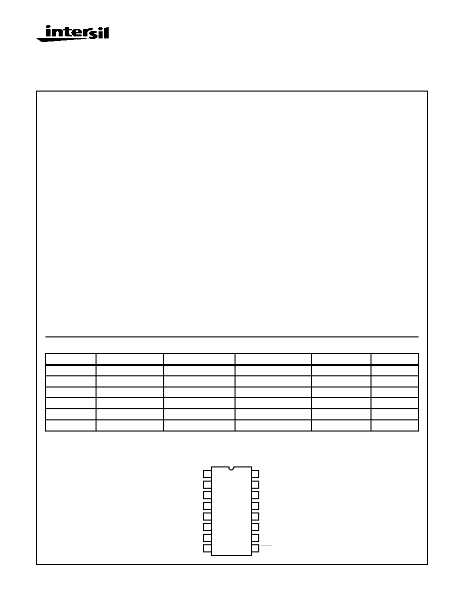
Pinout
CA3304 (SBDIP, PDIP, SOIC)
TOP VIEW
PART NUMBER LINEARITY (INL, DNL)
SAMPLING RATE
TEMP. RANGE (
o
C)
PACKAGE
PKG. NO.
CA3304E
±
0.25 LSB
25MHz (40ns)
-40 to 85
16 Ld PDIP
E16.3
CA3304AE
±
0.125 LSB
25MHz (40ns)
-40 to 85
16 Ld PDIP
E16.3
CA3304M
±
0.25 LSB
25MHz (40ns)
-40 to 85
16 Ld SOIC (W)
M16.3
CA3304AM
±
0.125 LSB
25MHZ (40ns)
-40 to 85
16 Ld SOIC (W)
M16.3
CA3304D
±
0.25 LSB
25MHz (40ns)
-55 to 125
16 Ld SBDIP
D16.3
CA3304AD
±
0.125 LSB
25MHz (40ns)
-55 to 125
16 Ld SBDIP
D16.3
14
15
16
9
13
12
11
10
1
2
3
4
5
7
6
8
BIT 1 (LSB)
BIT 2
BIT 3
BIT 4
DATA CHANGE (DC)
OVERFLOW (OF)
V
SS
CE2
V
DD
V
AA
-
V
REF
-
V
REF
+
V
IN
V
AA
+
CE1
CLK
File Number
1790.2
CAUTION: These devices are sensitive to electrostatic discharge; follow proper IC Handling Procedures.
1-888-INTERSIL or 321-724-7143 | Copyright © Intersil Corporation 1999

4-8
Absolute Maximum Ratings
Thermal Information
DC Supply Voltage Range (V
DD
or V
AA
+)
(Voltage Referenced to V
SS
or V
AA
- Terminal,
Whichever is More Negative) . . . . . . . . . . . . . . . . . . -0.5V to +8V
Input Voltage Range
CE1, CE2 Inputs . . . . . . . . . . . . . . . . . . . V
SS
-0.5V to V
DD
+0.5V
Clock, V
REF
+, V
REF
-, V
IN
Inputs . . . . . V
AA
- -0.5V to V
AA
- +0.5V
DC Input Current, Any Input . . . . . . . . . . . . . . . . . . . . . . . . .
±
20mA
Operating Conditions
Recommended Supply Voltage Range (V
DD
or V
AA
+) . . . . .3V to 7.5V
Recommended V
AA
+ Voltage Range . . . . . . V
DD
-1V to V
DD
+2.5V
Recommended V
AA
- Voltage Range . . . . . . . V
SS
-2.5V to V
SS
+1V
Operating Temperature
CA3304D . . . . . . . . . . . . . . . . . . . . . . . . . . . . . . . -55
o
C to 125
o
C
CA3304E, CA3304M. . . . . . . . . . . . . . . . . . . . . . . . -40
o
C to 85
o
C
Thermal Resistance (Typical, Note 1)
JA
(
o
C/W)
JC
(
o
C/W)
SBDIP Package . . . . . . . . . . . . . . . . . . . .
80
22
PDIP Package . . . . . . . . . . . . . . . . . . . . .
90
N/A
SOIC Package . . . . . . . . . . . . . . . . . . . . .
100
N/A
Maximum Junction Temperature
Ceramic Package . . . . . . . . . . . . . . . . . . . . . . . . . . . . . . . . 175
o
C
Plastic Package . . . . . . . . . . . . . . . . . . . . . . . . . . . . . . . . . . 150
o
C
Maximum Storage Temperature Range (T
STG
) . . . -65
o
C to 150
o
C
Maximum Lead Temperature (Soldering 10s) . . . . . . . . . . . . . 300
o
C
(SOIC - Lead Tips Only)
CAUTION: Stresses above those listed in "Absolute Maximum Ratings" may cause permanent damage to the device. This is a stress only rating and operation
of the device at these or any other conditions above those indicated in the operational sections of this specification is not implied.
NOTE:
1.
JA
is measured with the component mounted on an evaluation PC board in free air.
Electrical Specifications
T
A
= 25
o
C, V
REF
+ = 2V, V
DD
= V
AA
+ = 5V, V
AA
- = V
REF
- = V
SS
= GND, f
CLK
= 25MHz
Unless Otherwise Specified
PARAMETER
TEST CONDITIONS
MIN
TYP
MAX
UNITS
SYSTEM PERFORMANCE
Resolution
4
-
-
Bits
Input Errors
Integral Linearity
Error
CA3304A
-
±
0.1
±
0.125
LSB
CA3304
-
±
0.125
±
0.25
LSB
Differential Linearity
Error
CA3304A
-
±
0.1
±
0.125
LSB
CA3304
-
±
0.125
±
0.25
LSB
Offset Error
(Unadjusted)
CA3304A
-
-
±
0.75
LSB
CA3304
-
-
±
1.0
LSB
Gain Error
(Unadjusted)
CA3304A
-
-
±
0.75
LSB
CA3304
-
-
±
1.0
LSB
DYNAMIC CHARACTERISTICS (Input Signal Level 0.5dB Below Full Scale)
Conversion Timing
Aperture Delay
-
3
-
ns
Signal to Noise Ratio, SNR
RMS Signal
RMS Noise
f
S
= 25MHz, f
IN
= 100kHz
-
23.7
-
dB
f
S
= 25MHz, f
IN
= 5MHz
-
23.6
-
dB
Signal to Noise Ratio, SINAD
RMS Signal
RMS Noise + Distortion
f
S
= 25MHz, f
IN
= 100kHz
-
23.4
-
dB
f
S
= 25MHz, f
IN
= 5MHz
-
22.8
-
dB
Total Harmonic Distortion, THD
f
S
= 25MHz, f
IN
= 100kHz
-
-34.5
-
dBc
f
S
= 25MHz, f
IN
= 5MHz
-
-31.0
-
dBc
Effective Number of Bits, ENOB
f
S
= 25MHz, f
IN
= 100kHz
-
3.67
-
Bits
f
S
= 25MHz, f
IN
= 5MHz
-
3.57
-
Bits
ANALOG INPUTS
Input Range
Full Scale Input Range
(Notes 1, 4)
0.5
-
V
AA
V
Input Loading
Input Capacitance
-
10
-
pF
Input Current
V
IN
= 2V (Note 2)
-
150
200
µ
A
=
=
CA3304, CA3304A
4-9
Allowable Input Bandwidth
(Note 4)
-
25
f
CLK
/2
MHz
-3dB Input Bandwidth
-
40
-
MHz
REFERENCE INPUTS
Input Range
V
REF
+ Range
(Note 4)
V
AA
- +0.5
-
V
AA
+
V
V
REF
- Range
(Note 4)
V
AA
-
-
V
AA
+ -0.5
V
Input Loading
Resistor Ladder Impedance
V
IN
= 5V, CLK = Low
640
-
960
DIGITAL INPUTS
Digital Input
Maximum V
IN
, Low
CLOCK
(Notes 3, 4)
-
-
0.3 x V
AA
V
CE1, CE2
(Note 4)
-
-
0.3 x V
DD
V
Minimum V
IN
, High
CLOCK
(Notes 3, 4)
0.7 x V
AA
-
-
V
CE1, CE2
(Note 4)
0.7 x V
DD
-
-
V
Input Leakage, Except CLK
V = 0V, 5V
-
-
±
1
µ
A
Input Leakage, CLK
(Note 3)
-
±
100
±
150
µ
A
DIGITAL OUTPUTS
Digital Outputs
Output Low (Sink) Current
V
O
= 0.4V
6
-
-
mA
Output High (Source) Current
V
O
= 4.6V
-3
-
-
mA
Three-State Leakage Current
V
O
= 0V, 5V
-
±
0.2
±
5
µ
A
TIMING CHARACTERISTICS
Conversion Timing
Maximum Conversion Speed
CLK = Square Wave
25
35
-
MSPS
Auto-Balance Time (
1)
20
-
-
ns
Sample Time (
2)
20
-
5000
ns
Output Timing
Data Valid Delay
(Note 4)
-
30
40
ns
Data Hold Time
(Note 4)
15
25
-
ns
Output Enable Time
-
15
-
ns
Output Disable Time
-
10
-
ns
POWER SUPPLY CHARACTERISTICS
Device Current, I
AA
Continuous Clock
-
5.5
-
mA
Continuous
2
-
0.4
-
mA
Continuous
1
-
2
-
mA
Device Current, I
DD
Continuous Clock
-
1.5
-
mA
V
AA
+ = 5V,
V
SS
= CE1 = V
AA
- = CLK = GND
Continuous
2
-
5
10
mA
V
AA
+ = 7V
Continuous
1
-
5
20
mA
NOTES:
1. Full scale input range, V
REF
+ - V
REF
-, may be in the range of 0.5V to V
AA
+ -V
AA
- volts. Linearity errors increase at lower full scale ranges,
however.
2. Input current is due to energy transferred to the input at the start of the sample period. The average value is dependent on input and VDD
voltage.
3. The CLK input is a CMOS inverter with a 50k
feedback resistor. It operates from the V
AA
+ and V
AA
- supplies. It may be AC-coupled
with a 1V
P-P
minimum source.
4. Parameter not tested, but guaranteed by design or characterization.
Electrical Specifications
T
A
= 25
o
C, V
REF
+ = 2V, V
DD
= V
AA
+ = 5V, V
AA
- = V
REF
- = V
SS
= GND, f
CLK
= 25MHz
Unless Otherwise Specified (Continued)
PARAMETER
TEST CONDITIONS
MIN
TYP
MAX
UNITS
CA3304, CA3304A

4-10
Pin Descriptions
PIN NUMBER
NAME
DESCRIPTION
1
Bit 1
Bit 1 (LSB).
Output Data Bits
(High = True)
2
Bit 2
Bit 2.
3
Bit 3
Bit 3.
4
Bit 4
Bit 4 (MSB).
5
DC
Data Change.
6
OF
Overflow.
7
CE2
Three-State Output Enable Input, active low. See the Chip Enable Truth Table.
8
V
SS
Digital Ground.
9
CE1
Three-State Output Enable Input, active high. See the Chip Enable Truth Table.
10
V
AA
+
Analog Power Supply, +5V.
11
V
IN
Analog Signal Input.
12
V
REF
+
Reference Voltage Positive Input.
13
V
REF
-
Reference Voltage Negative Input.
14
V
AA
-
Analog Ground.
15
CLK
Clock Input.
16
V
DD
Digital Power Supply, +5V.
CHIP ENABLE TRUTH TABLE
CE1
CE2
BIT 1 - BIT 4
DC, OF
0
1
Valid
Valid
1
1
Three-State
Valid
X
0
Three-State
Three-State
X = Don't Care
TABLE 1. OUTPUT CODE TABLE
CODE
DESCRIPTION
INPUT VOLTAGE (V)
OUTPUT CODE
DECIMAL
COUNT
V
REF
+ = 1V
V
REF
- = -1V
1.6V
0V
2V
0V
3.2V
0V
4.8V
0V
OF
B4
B3
B2
B1
Zero
-1.000
0
0
0
0
0
0
0
0
0
0
1 LSB
-0.875
0.1
0.125
0.2
0.3
0
0
0
0
1
1
2 LSB
-0.750
0.2
0.250
0.4
0.6
0
0
0
1
0
2
∑
∑
∑
∑
∑
∑
∑
∑
∑
∑
∑
∑
∑
∑
∑
∑
∑
∑
∑
∑
∑
∑
∑
∑
∑
∑
∑
∑
∑
∑
∑
∑
∑
∑
∑
∑
∑
∑
∑
∑
∑
∑
∑
∑
∑
∑
∑
∑
1
/
2
Full Scale -1 LSB
-0.125
0.7
0.875
1.4
2.1
0
0
1
1
1
7
1
/
2
Full Scale
0
0.8
1.000
1.6
2.4
0
1
0
0
0
8
1
/
2
Full Scale +1 LSB
0.125
0.9
1.125
1.8
2.7
0
1
0
0
1
9
∑
∑
∑
∑
∑
∑
∑
∑
∑
∑
∑
∑
∑
∑
∑
∑
∑
∑
∑
∑
∑
∑
∑
∑
∑
∑
∑
∑
∑
∑
∑
∑
∑
∑
∑
∑
∑
∑
∑
∑
∑
∑
∑
∑
∑
∑
∑
∑
Full Scale -1 LSB
0.750
1.4
1.750
2.8
4.2
0
1
1
1
0
14
Full Scale
0.875
1.5
1.875
3.0
4.5
0
1
1
1
1
15
Overflow
1.000
1.6
2.000
3.2
4.8
1
1
1
1
1
31
Step Size
0.125
0.1
0.125
0.2
0.3
NOTE:
1. The voltages listed are the ideal centers of each output code shown as a function of its associated reference voltage See Ideal Transfer
Curve Figure 6. The output code should exist for an input equal to the ideal center voltage
±
1
/
2
of the step size.
CA3304, CA3304A
4-11
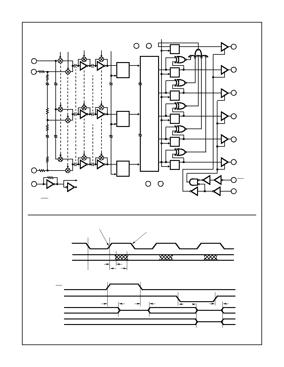
Functional Diagram
Timing Diagrams
FIGURE 1. TIMING DIAGRAM
FIGURE 2. OUTPUT ENABLE/DISABLE TIMING
Cascaded Auto Balance (CAB)
NOTE: CE1 and CE2 inputs and data outputs have standard CMOS protection networks to V
DD
and V
SS
. Analog inputs and clock have
standard CMOS protection networks to V
AA
+ and V
AA
-.
9
7
1
D Q
CLK
D Q
CLK
D Q
CLK
D Q
CLK
D Q
CLK
D Q
CLK
5
2
3
4
6
ENCODER
LOGIC
ARRAY
D
LATCH
16
Q
COUNT
16
COUNT
8
D
LATCH
8
Q
D
LATCH
0
Q
COUNT
1
8
14
V
AA
-
V
SS
CAB COMPARATOR #1
1 (AUTO BALANCE)
2 (SAMPLE UNKNOWN)
50k
CLOCK
15
13
V
REF
-
V
REF
+
V
IN
12
11
16
10
V
AA
+
V
DD
1
1
1
1
2
2
1
/
2
R
1
/
2
R
R
R
R
CAB #8
CAB #16
OUTPUT
REGISTER
THREE-STATE
DRIVERS
DATA
CHANGE
OVERFLOW
BIT 4
BIT 3
BIT 2
BIT 1 (LSB)
CE1
CE2
R
CLOCK
B1 - B4, DC & OF
COMPARATOR DATA
DATA VALID 2
1
2
t
HO
1
1
0
0
AUTO
BALANCE
AUTO
BALANCE
AUTO
BALANCE
SAMPLE 1
SAMPLE 2
SAMPLE 3
LATCHED
DATA SHIFTED INTO
OUTPUT REGISTERS
DATA VALID 1
DATA VALID 0
t
D
BITS 1-4
DC, OF
t
DIS
HIGH
CE2
CE1
IMPEDANCE
HIGH
IMPEDANCE
HIGH
IMPEDANCE
t
EN
t
EN
t
DIS
CA3304, CA3304A