 | –≠–ª–µ–∫—Ç—Ä–æ–Ω–Ω—ã–π –∫–æ–º–ø–æ–Ω–µ–Ω—Ç: CA3306J3 | –°–∫–∞—á–∞—Ç—å:  PDF PDF  ZIP ZIP |
4-8
CA3306, CA3306A,
CA3306C
6-Bit, 15 MSPS,
Flash A/D Converters
August 1997
File Number
3102.1
Features
∑ CMOS Low Power with Video Speed (Typ) . . . . .70mW
∑ Parallel Conversion Technique
∑ Signal Power Supply Voltage . . . . . . . . . . . . 3V to 7.5V
∑ 15MHz Sampling Rate with Single 5V Supply
∑ 6-Bit Latched Three-State Output with Overflow Bit
∑ Pin-for-Pin Retrofit for the CA3300
Applications
∑ TV Video Digitizing
∑ Ultrasound Signature Analysis
∑ Transient Signal Analysis
∑ High Energy Physics Research
∑ High Speed Oscilloscope Storage/Display
∑ General Purpose Hybrid ADCs
∑ Optical Character Recognition
∑ Radar Pulse Analysis
∑ Motion Signature Analysis
∑ Robot Vision
Description
The CA3306 family are CMOS parallel (FLASH) analog-to-digital
converters designed for applications demanding both low power
consumption and high speed digitization. Digitizing at 15MHz, for
example, requires only about 50mW.
The CA3306 family operates over a wide, full scale signal input volt-
age range of 1V up to the supply voltage. Power consumption is as
low as 15mW, depending upon the clock frequency selected. The
CA3306 types may be directly retrofitted into CA3300 sockets, offer-
ing improved linearity at a lower reference voltage and high operat-
ing speed with a 5V supply.
The intrinsic high conversion rate makes the CA3306 types ideally
suited for digitizing high speed signals. The overflow bit makes pos-
sible the connection of two or more CA3306s in series to increase
the resolution of the conversion system. A series connection of two
CA3306s may be used to produce a 7-bit high speed converter.
Operation of two CA3306s in parallel doubles the conversion speed
(i.e., increases the sampling rate from 15MHz to 30MHz).
Sixty-four paralleled auto balanced comparators measure the input
voltage with respect to a known reference to produce the parallel bit
outputs in the CA3306. Sixty-three comparators are required to
quantize all input voltage levels in this 6-bit converter, and the addi-
tional comparator is required for the overflow bit.
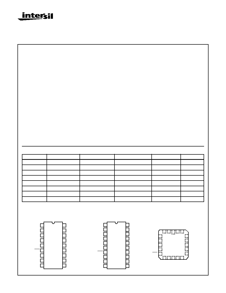
Ordering Information
Pinouts
PART NUMBER LINEARITY (INL, DNL)
SAMPLING RATE
TEMP. RANGE (
o
C)
PACKAGE
PKG. NO.
CA3306E
±
0.5 LSB
15MHz (67ns)
-40 to 85
18 Ld PDIP
E18.3
CA3306CE
±
0.5 LSB
10MHz (100ns)
-40 to 85
18 Ld PDIP
E18.3
CA3306M
±
0.5 LSB
15MHz (67ns)
-40 to 85
20 Ld SOIC
M20.3
CA3306CM
±
0.5 LSB
10MHz (100ns)
-40 to 85
20 Ld SOIC
M20.3
CA3306D
±
0.5 LSB
15MHz (67ns)
-55 to 125
18 Ld SBDIP
D18.3
CA3306CD
±
0.5 LSB
10MHz (100ns)
-55 to 125
18 Ld SBDIP
D18.3
CA3306J3
±
0.5 LSB
15MHz (67ns)
-55 to 125
20 Ld CLCC
J20.B
CA3306J3
±
0.5 LSB
10MHz (100ns)
-55 to 125
20 Ld CLCC
J20.B
CA3306 (PDIP, SBDIP)
TOP VIEW
CA3306 (SOIC)
TOP VIEW
CA3306 (CLCC)
TOP VIEW
10
11
12
13
14
15
16
17
18
9
8
7
6
5
4
3
2
1
(MSB) B6
OVERFLOW
V
SS
V
Z
CE2
CLK
CE2
PHASE
V
REF
+
B5
REF
B3
B2
B4
B1 (LSB)
V
DD
V
IN
V
REF
-
CENTER
11
12
13
14
15
16
17
18
20
19
10
9
8
7
6
5
4
3
2
1
(MSB) B6
OVERFLOW
V
SS
NC
V
Z
CE2
CLK
CE1
PHASE
V
REF
+
B5
REF
B3
B2
B4
B1 (LSB)
V
DD
NC
V
IN
V
REF
-
CENTER
4
5
6
7
8
9 10 11 12 13
3
2
1 20 19
15
14
18
17
16
V
SS
V
Z
NC
CE2
CE1
REF
B3
B1 (LSB)
V
DD
B2
B5
B4
NC
CLK
V
REF
+
V
REF
-
PHASE
V
IN
B6
O
VER-
CENTER
FLO
W
(MSB)
CAUTION: These devices are sensitive to electrostatic discharge; follow proper IC Handling Procedures.
http://www.intersil.com or 407-727-9207
|
Copyright
©
Intersil Corporation 1999
4-9
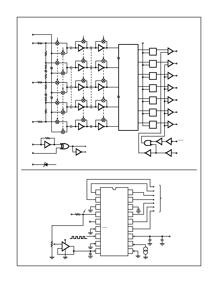
Functional Block Diagram
Typical Application Circuit
ENCODER
LOGIC
COMP
1
V
SS
1 (AUTO BALANCE)
2 (SAMPLE UNKNOWN)
50k
CLOCK
V
REF
-
V
REF
+
V
IN
V
DD
1
1
1
2
2
R
R/2
R
R
R
THREE-STATE
R/2
D Q
CL
D Q
CL
D Q
CL
D Q
CL
D Q
CL
D Q
CL
D Q
CL
AND
LATCHES
COMPARATOR
COMP
2
COMP
32
COMP
63
COMP
64
REF
CENTER
120
R
R
PHASE
ZENER
DIODE
V
SS
6.2V NOMINAL
OVERFLOW
CE1
CE2
B6 (MSB)
B5
B4
B3
B2
B1 (LSB)
B6
OF
V
SS
V
Z
CE2
CLK
CE1
PH
V
REF+
B5
RC
B3
B2
B4
B1
V
DD
V
IN
V
REF-
CLOCK
CA741CE
+12V
560
5k
+5V
6.2V
+12V
0.1
µ
F
+
-
0.2
µ
F
10
µ
F
+5V
SIGNAL
INPUT
DATA
OUTPUT
OF
B6
B5
B4
B3
B2
B1
(LSB)
0.1
µ
F
10
11
12
13
14
15
16
17
18
9
8
7
6
5
4
3
2
1
CA3306
CA3306, CA3306A, CA3306C
4-10
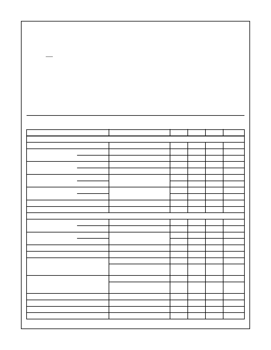
Absolute Maximum Ratings
Thermal Information
DC Supply Voltage Range, V
DD
Voltage Referenced to V
SS
Terminal . . . . . . . . . . . -0.5V to +8.5V
Input Voltage Range
All Inputs Except Zener. . . . . . . . . . . . . . . . . -0.5V to V
DD
+ 0.5V
DC Input Current
CLK, PH, CE1, CE2, V
IN
. . . . . . . . . . . . . . . . . . . . . . . . .
±
20mA
Operating Conditions
Supply Voltage Range . . . . . . . . . . . . . . . . . . . . . . . . . . . . .3V to 8V
Temperature Range (T
A
)
Ceramic Package (D Suffix) . . . . . . . . . . . . . . . . . -55
o
C to 125
o
C
Plastic Package (E or M Suffix). . . . . . . . . . . . . . . . -40
o
C to 85
o
C
Thermal Resistance (Typical, Note 1)
JA
(
o
C/W)
JC
(
o
C/W)
SBDIP Package . . . . . . . . . . . . . . . . . . . .
75
24
PDIP Package . . . . . . . . . . . . . . . . . . . . .
95
N/A
SOIC Package . . . . . . . . . . . . . . . . . . . . .
115
N/A
CLCC Package . . . . . . . . . . . . . . . . . . . .
80
28
Maximum Junction Temperature
Hermetic Packages . . . . . . . . . . . . . . . . . . . . . . . . . . . . . . . 175
o
C
Plastic Packages . . . . . . . . . . . . . . . . . . . . . . . . . . . . . . . . . 150
o
C
Maximum Storage Temperature Range . . . . . . . . . .-65
o
C to 150
o
C
Maximum Lead Temperature (Soldering 10s) . . . . . . . . . . . . . 300
o
C
(SOIC - Lead Tips Only)
CAUTION: Stresses above those listed in "Absolute Maximum Ratings" may cause permanent damage to the device. This is a stress only rating and operation
of the device at these or any other conditions above those indicated in the operational sections of this specification is not implied.
NOTE:
1.
JA
is measured with the component mounted on an evaluation PC board in free air.
Electrical Specifications
T
A
= 25
o
C, V
DD
= 5V, V
REF
+ = 4.8V, V
SS
= V
REF
- = GND, Clock = 15MHz Square Wave for CA3306 or
CA3306A, 10MHz for CA3306C
PARAMETER
TEST CONDITIONS
MIN
TYP
MAX
UNITS
SYSTEM PERFORMANCE
Resolution
6
-
-
Bits
Integral Linearity Error, INL
CA3306, CA3306C
-
±
0.25
±
0.5
LSB
CA3306A
-
±
0.2
±
0.25
LSB
Differential Linearity Error,
DNL
CA3306, CA3306C
-
±
0.25
±
0.5
LSB
CA3306A
-
±
0.2
±
0.25
LSB
Offset Error (Unadjusted)
CA3306, CA3306C (Note 1)
-
±
0.5
±
1
LSB
CA3306A
-
±
0.25
±
0.5
LSB
Gain Error (Unadjusted)
CA3306, CA3306C (Note 2)
-
±
0.5
±
1
LSB
CA3306A
-
±
0.25
±
0.5
LSB
Gain Temperature Coefficient
-
+0.1
-
mV/
o
C
Offset Temperature Coefficient
-
-0.1
-
mV/
o
C
DYNAMIC CHARACTERISTICS (Input Signal Level 0.5dB Below Full Scale)
Maximum Conversion Speed
CA3306C
10
13
-
MSPS
CA3306, CA3306A
15
20
-
MSPS
Maximum Conversion Speed
CA3306C
(Note 4)
1,
2
Minimum
12
-
-
MSPS
CA3306, CA3306A
18
-
-
MSPS
Allowable Input Bandwidth
(Note 4)
DC
-
f
CLOCK/2
MHz
-3dB Input Bandwidth
-
30
-
MHz
Signal to Noise Ratio, SNR
f
S
= 15MHz, f
IN
= 100kHz
-
34.6
-
dB
f
S
= 15MHz, f
IN
= 5MHz
-
33.4
-
dB
Signal to Noise Ratio, SINAD
f
S
= 15MHz, f
IN
= 100kHz
-
34.2
-
dB
f
S
= 15MHz, f
IN
= 5MHz
-
29.0
-
dB
Total Harmonic Distortion, THD
f
S
= 15MHz, f
IN
= 100kHz
-
-46.0
-
dBc
f
S
= 15MHz, f
IN
= 5MHz
-
-30.0
-
dBc
Effective Number of Bits, ENOB
f
S
= 15MHz, f
IN
= 100kHz
-
5.5
-
Bits
f
S
= 15MHz, f
IN
= 5MHz
-
4.5
-
Bits
=
RMSSignal
RMSNoise
--------------------------------
=
RMSSignal
RMSNoise+Distortion
------------------------------------------------------------
CA3306, CA3306A, CA3306C
4-11
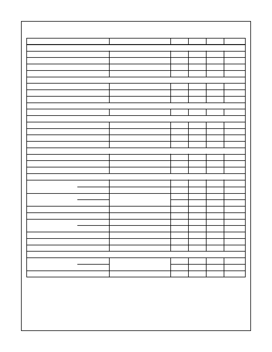
ANALOG INPUTS
Positive Full Scale Input Range
(Notes 3, 4)
1
4.8
V
DD
+ 0.5
V
Negative Full Scale Input Range
(Notes 3, 4)
-0.5
0
V
DD
- 1
V
Input Capacitance
-
15
-
pF
Input Current
V
IN
= 4.92V, V
DD
= 5V
-
-
±
500
µ
A
INTERNAL VOLTAGE REFERENCE
Zener Voltage
I
Z
= 10mA
5.4
6.2
7.4
V
Zener Dynamic Impedance
I
Z
= 10mA, 20mA
-
12
25
Zener Temperature Coefficient
-
-0.5
-
mV/
o
C
REFERENCE INPUTS
Resistor Ladder Impedance
650
1100
1550
DIGITAL INPUTS
Maximum V
IN
, Logic 0
All Digital Inputs (Note 4)
-
-
0.3 x V
DD
V
Maximum V
IN
, Logic 1
All Digital Inputs (Note 4)
0.7 x V
DD
-
-
V
Digital Input Current
Except CLK, V
IN
= 0V, 5V
-
±
1
±
5
µ
A
Digital Input Current
CLK Only
-
±
100
±
200
µ
A
DIGITAL OUTPUTS
Digital Output Three-State Leakage
V
OUT
= 0V, 5V
-
±
1
±
5
µ
A
Digital Output Source Current
V
OUT
= 4.6V
-1.6
-
-
mA
Digital Output Sink Current
V
OUT
= 0.4V
3.2
-
-
mA
TIMING CHARACTERISTICS
Auto Balance Time (
1)
CA3306C
50
-
ns
CA3306, CA3306A
33
-
Sample Time (
2)
CA3306C
(Note 4)
33
-
5000
ns
CA3306, CA3306A
22
-
5000
ns
Aperture Delay
-
8
-
ns
Aperture Jitter
-
100
-
ps
P-P
Output Data Valid Delay, t
D
CA3306C
-
35
50
ns
CA3306, CA3306A
-
30
40
ns
Output Data Hold Time, t
H
(Note 4)
15
25
-
ns
Output Enable Time, t
EN
-
20
-
ns
Output Disable Time, t
DIS
-
15
-
ns
POWER SUPPLY CHARACTERISTICS
I
DD
Current, Refer to Figure 4 CA3306C
Continuous Conversion (Note 4)
-
11
20
mA
CA3306, CA3306A
-
14
25
mA
I
DD
Current
Continuous
1
-
7.5
15
mA
NOTES:
1. OFFSET ERROR is the difference between the input voltage that causes the 00 to 01 output code transition and (V
REF
+ - V
REF
-)/128.
2. GAIN ERROR is the difference the input voltage that causes the 3F
16
to overflow output code transition and (V
REF
+ - V
REF
-) x 127/128.
3. The total input voltage range, set by V
REF
+ and V
REF
-, may be in the range of 1 to (V
DD
+ 1) V.
4. Parameter not tested, but guaranteed by design or characterization.
Electrical Specifications
T
A
= 25
o
C, V
DD
= 5V, V
REF
+ = 4.8V, V
SS
= V
REF
- = GND, Clock = 15MHz Square Wave for CA3306 or
CA3306A, 10MHz for CA3306C (Continued)
PARAMETER
TEST CONDITIONS
MIN
TYP
MAX
UNITS
CA3306, CA3306A, CA3306C

4-12
Timing Waveforms
FIGURE 1. INPUT-TO-OUTPUT
FIGURE 2. OUTPUT ENABLE
FIGURE 3. PULSE MODE
CLOCK IF
PHASE IS HIGH
CLOCK IF
PHASE IS LOW
COMPARATOR DATA IS LATCHED
DECODED DATA IS SHIFTED TO OUTPUT REGISTERS
AUTO
BALANCE
AUTO
BALANCE
SAMPLE
N + 2
SAMPLE
N + 1
2
2
2
1
1
t
D
t
H
DATA
N - 2
DATA
N - 1
DATA
N
t
DIS
t
EN
t
DIS
t
DIS
CE1
CE2
BITS 1-6
OF
DATA
HIGH
IMPEDANCE
HIGH
IMPEDANCE
HIGH
IMPEDANCE
DATA
DATA
DATA
DATA
2
1
2
t
D
OLD DATA
NEW DATA
FIGURE 3A.
t
D
2
1
1
2
1
OLD
DATA
OLD
DATA +1
NEW
DATA
SAMPLE ENDS
CLOCK
OUTPUT
FIGURE 3B.
CLOCK
OUTPUT
t
D
2
1
2
1
INVALID
DATA
NEW
DATA
CLOCK
OLD DATA
FIGURE 3C.
2
OUTPUT
SAMPLE ENDS
SAMPLE ENDS
CA3306, CA3306A, CA3306C