 | –≠–ª–µ–∫—Ç—Ä–æ–Ω–Ω—ã–π –∫–æ–º–ø–æ–Ω–µ–Ω—Ç: CA3338M | –°–∫–∞—á–∞—Ç—å:  PDF PDF  ZIP ZIP |
10-11
August 1997
CA3338, CA3338A
CMOS Video Speed, 8-Bit,
50 MSPS, R2R D/A Converters
Features
∑ CMOS/SOS Low Power
∑ R2R Output, Segmented for Low "Glitch"
∑ CMOS/TTL Compatible Inputs
∑ Fast Settling: (Typ) to
1
/
2
LSB . . . . . . . . . . . . . . . . 20ns
∑ Feedthrough Latch for Clocked or Unclocked Use
∑ Accuracy (Typ) . . . . . . . . . . . . . . . . . . . . . . . . .
±
0.5 LSB
∑ Data Complement Control
∑ High Update Rate (Typ) . . . . . . . . . . . . . . . . . . . . 50MHz
∑ Unipolar or Bipolar Operation
Applications
∑ TV/Video Display
∑ High Speed Oscilloscope Display
∑ Digital Waveform Generator
∑ Direct Digital Synthesis
Description
The CA3338 family are CMOS/SOS high speed R2R voltage
output digital-to-analog converters. They can operate from a
single +5V supply, at video speeds, and can produce
"rail-to-rail" output swings. Internal level shifters and a pin for
an optional second supply provide for an output range below
digital ground. The data complement control allows the inver-
sion of input data while the latch enable control provides
either feedthrough or latched operation. Both ends of the
R2R ladder network are available externally and may be
modulated for gain or offset adjustments. In addition, "glitch"
energy has been kept very low by segmenting and thermom-
eter encoding of the upper 3 bits.
The CA3338 is manufactured on a sapphire substrate to give
low dynamic power dissipation, low output capacitance, and
inherent latch-up resistance.
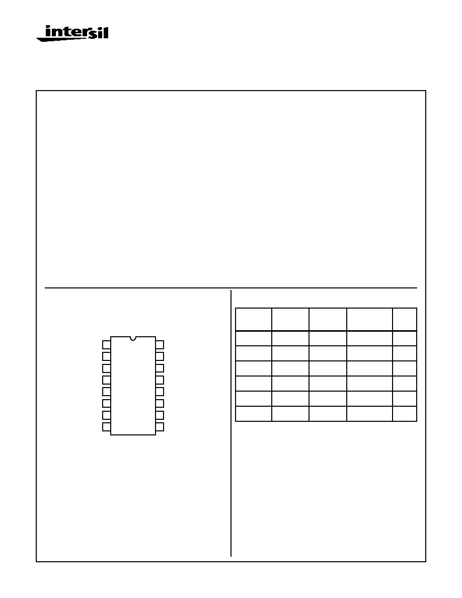
Pinout
CA3338, CA3338A
(PDIP, SBDIP, SOIC)
TOP VIEW
Ordering Information
14
15
16
9
13
12
11
10
1
2
3
4
5
7
6
8
D7
D6
D5
D4
D3
D2
V
SS
D1
V
DD
COMP
V
REF
+
V
OUT
V
REF
-
V
EE
D0
LE
PART
NUMBER
LINEARITY
(INL, DNL)
TEMP.
RANGE (
o
C)
PACKAGE
PKG.
NO.
CA3338E
±
1.0 LSB
-40 to 85
16 Ld PDIP
E16.3
CA3338AE
±
0.75 LSB
-40 to 85
16 Ld PDIP
E16.3
CA3338D
±
1.0 LSB
-55 to 125
16 Ld SBDIP
D16.3
CA3338AD
±
0.75 LSB
-55 to 125
16 Ld SBDIP
D16.3
CA3338M
±
1.0 LSB
-40 to 85
16 Ld SOIC
M16.3
CA3338AM
±
0.75 LSB
-40 to 85
16 Ld SOIC
M16.3
File Number
1850.2
CAUTION: These devices are sensitive to electrostatic discharge; follow proper IC Handling Procedures.
http://www.intersil.com or 407-727-9207
|
Copyright
©
Intersil Corporation 1999
10-12
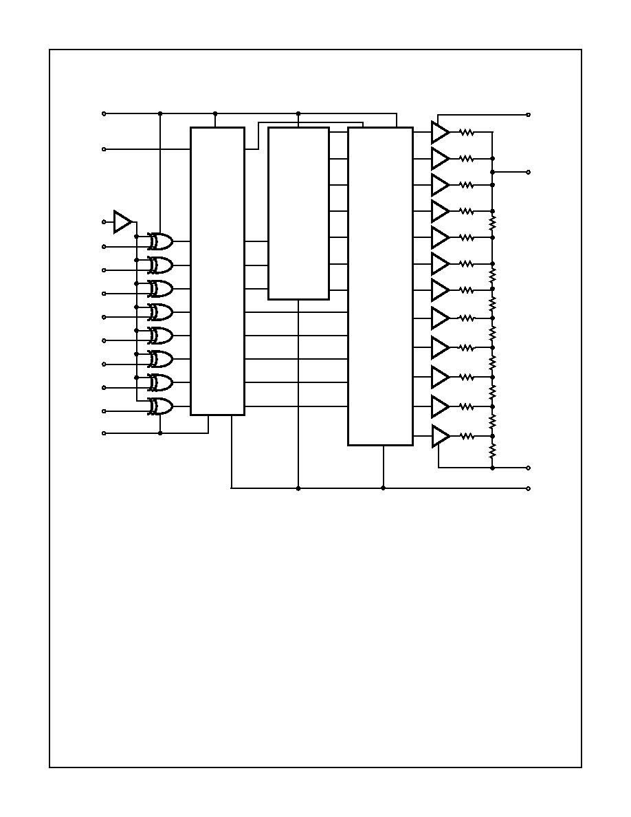
Functional Diagram
COMP
TO 7-LINE
V
DD
D7
D6
D5
D4
D3
D2
D1
D0
V
SS
16
15
14
1
2
3
4
5
6
7
9
8
THERMOMETER
ENCODER
3-BIT
LEVEL
SHIFTERS
FEEDTHROUGH
LATCHES
8R
4R
2R
2R
2R
2R
2R
2R
8R
8R
8R
4R
13
10
V
EE
V
REF
-
V
OUT
V
REF
+
12
11
2R
R
R
R
LE
R
160
R
R
R
R
CA3338, CA3338A
10-13
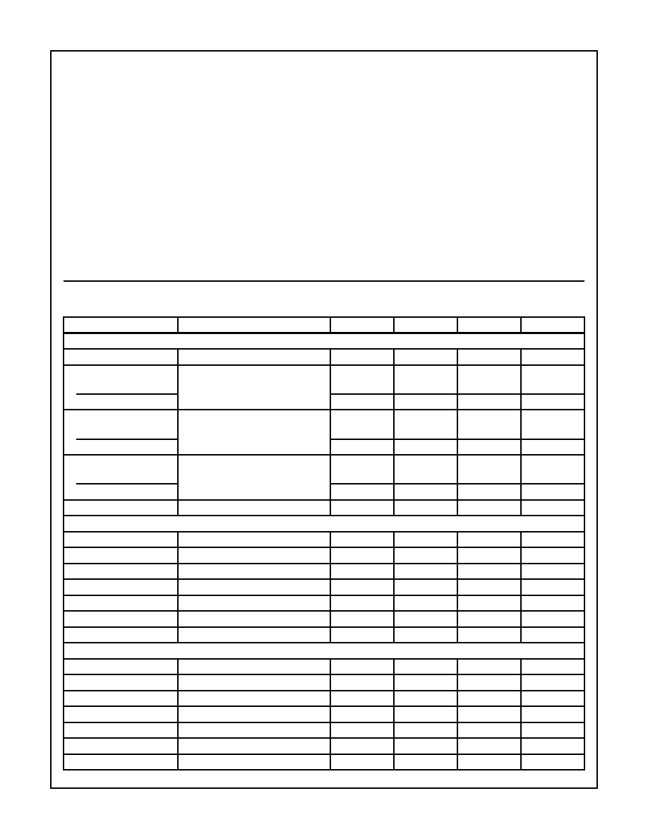
Absolute Maximum Ratings
Thermal Information
DC Supply-Voltage Range . . . . . . . . . . . . . . . . . . . . . . -0.5V to +8V
(V
DD
- V
SS
or V
DD
- V
EE
, Whichever is Greater)
Input Voltage Range
Digital Inputs (LE, COMP D0 - D7) . . . . V
SS
- 0.5V to V
DD
+ 0.5V
Analog Pins (V
REF
+, V
REF
-, V
OUT
) . . . . V
DD
- 8V to V
DD
+ 0.5V
DC Input Current
Digital Inputs (LE, COMP, D0 - D7). . . . . . . . . . . . . . . . . .
±
20mA
Recommended Supply Voltage Range. . . . . . . . . . . . . .4.5V to 7.5V
Operating Conditions
Temperature Range (T
A
)
Ceramic Package, D suffix . . . . . . . . . . . . . . . . . . . -55
o
C to 125
o
C
Plastic Package, E suffix, M suffix . . . . . . . . . . . . . . -40
o
C to 85
o
C
Thermal Resistance (Typical, Note 1)
JA
(
o
C/W)
JC
(
o
C/W)
SBDIP Package . . . . . . . . . . . . . . . . . .
75
24
PDIP Package . . . . . . . . . . . . . . . . . . .
100
N/A
SOIC Package . . . . . . . . . . . . . . . . . . .
100
N/A
Maximum Junction Temperature
Ceramic Package . . . . . . . . . . . . . . . . . . . . . . . . . . . . . . . . 175
o
C
Plastic Packages . . . . . . . . . . . . . . . . . . . . . . . . . . . . . . . . . 150
o
C
Maximum Storage Temperature Range, T
STG
. . . . .-65
o
C to 150
o
C
Maximum Lead Temperature (Soldering 10s) . . . . . . . . . . . . . 300
o
C
(SOIC - Lead Tips Only)
CAUTION: Stresses above those listed in "Absolute Maximum Ratings" may cause permanent damage to the device. This is a stress only rating and operation
of the device at these or any other conditions above those indicated in the operational sections of this specification is not implied.
NOTE:
1.
JA
is measured with the component mounted on an evaluation PC board in free air.
Electrical Specifications
T
A
= 25
o
C, V
DD
= 5V, V
REF
+ = 4.608V, V
SS
= V
EE
= V
REF
- = GND, LE Clocked at 20MHz, R
L
1 M
,
Unless Otherwise Specified
PARAMETER
TEST CONDITIONS
MIN
TYP
MAX
UNITS
ACCURACY
Resolution
8
-
-
Bits
Integral Linearity Error
See Figure 4
CA3338
-
-
±
1
LSB
CA3338A
-
-
±
0.75
LSB
Differential Linearity Error
See Figure 4
CA3338
-
-
±
0.75
LSB
CA3338A
-
-
±
0.5
LSB
Gain Error
Input Code = FF
HEX
, See Figure 3
CA3338
-
-
±
0.75
LSB
CA3338A
-
-
±
0.5
LSB
Offset Error
Input Code = 00
HEX
; See Figure 3
-
-
±
0.25
LSB
DIGITAL INPUT TIMING
Update Rate
To Maintain
1
/
2
LSB Settling
DC
50
-
MHz
Update Rate
V
REF
- = V
EE
= -2.5V, V
REF
+ = +2.5V
DC
20
-
MHz
Set Up Time t
SU1
For Low Glitch
-
-2
-
ns
Set Up Time t
SU2
For Data Store
-
8
-
ns
Hold Time t
H
For Data Store
-
5
-
ns
Latch Pulse Width t
W
For Data Store
-
5
-
ns
Latch Pulse Width t
W
V
REF
- = V
EE
= -2.5V, V
REF
+ = +2.5V
-
25
-
ns
OUTPUT PARAMETERS
R
L
Adjusted for 1V
P-P
Output
Output Delay t
D1
From LE Edge
-
25
-
ns
Output Delay t
D2
From Data Changing
-
22
-
ns
Rise Time t
r
10% to 90% of Output
-
4
-
ns
Settling Time t
S
10% to Settling to
1
/
2
LSB
-
20
-
ns
Output Impedance
V
REF
+ = 6V, V
DD
= 6V
120
160
200
Glitch Area
-
150
-
pV/s
Glitch Area
V
REF
- = V
EE
= -2.5V,V
REF
+ = +2.5V
-
250
-
pV/s
CA3338, CA3338A
10-14
Digital Signal Path
The digital inputs (LE, COMP, and D0 - D7) are of TTL
compatible HCT High Speed CMOS design: the loading is
essentially capacitive and the logic threshold is typically
1.5V.
The 8 data bits, D0 (weighted 2
0
) through D7 (weighted 2
7
),
are applied to Exclusive OR gates (see Functional Diagram).
The COMP (data complement) control provides the second
input to the gates: if COMP is high, the data bits will be
inverted as they pass through.
The input data and the LE (latch enable) signals are next
applied to a level shifter. The inputs, operating between the
levels of V
DD
and V
SS
, are shifted to operate between V
DD
and V
EE
. V
EE
optionally at ground or at a negative voltage,
will be discussed under bipolar operation. All further logic
elements except the output drivers operate from the V
DD
and V
EE
supplies.
The upper 3 bits of data, D5 through D7, are input to a 3-to-7
line bar graph encoder. The encoder outputs and D0 through
D4 are applied to a feedthrough latch, which is controlled by
LE (latch enable).
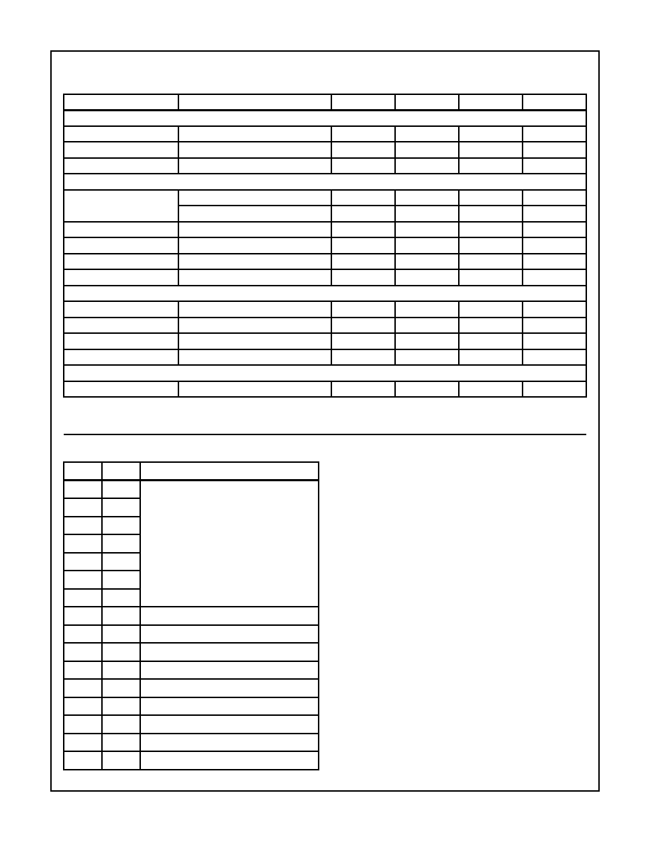
REFERENCE VOLTAGE
V
REF
+ Range
(+) Full Scale, Note 1
V
REF
- + 3
-
V
DD
V
V
REF
- Range
(-) Full Scale, Note 1
V
EE
-
V
REF
+ - 3
V
V
REF
+ Input Current
V
REF
+ = 6V, V
DD
= 6V
-
40
50
mA
SUPPLY VOLTAGE
Static I
DD
or I
EE
LE = Low, D0 - D7 = High
-
100
220
µ
A
LE = Low, D0 - D7 = Low
-
-
100
µ
A
Dynamic I
DD
or I
EE
V
OUT
= 10MHz, 0V to 5V Square Wave
-
20
-
mA
Dynamic I
DD
or I
EE
V
OUT
= 10MHz,
±
2.5V Square Wave
-
25
-
mA
V
DD
Rejection
50kHz Sine Wave Applied
-
3
-
mV/V
V
EE
Rejection
50kHz Sine Wave Applied
-
1
-
mV/V
DIGITAL INPUTS
D0 - D7, LE, COMP
High Level Input Voltage
Note 1
2
-
-
V
Low Level Input Voltage
Note 1
-
-
0.8
V
Leakage Current
-
±
1
±
5
µ
A
Capacitance
-
5
-
pF
TEMPERATURE COEFFICIENTS
Output Impedance
-
200
-
ppm/
o
C
NOTE:
1. Parameter not tested. but guaranteed by design or characterization.
Electrical Specifications
T
A
= 25
o
C, V
DD
= 5V, V
REF
+ = 4.608V, V
SS
= V
EE
= V
REF
- = GND, LE Clocked at 20MHz, R
L
1 M
,
Unless Otherwise Specified (Continued)
PARAMETER
TEST CONDITIONS
MIN
TYP
MAX
UNITS
Pin Descriptions
PIN
NAME
DESCRIPTION
1
D7
Most Significant Bit
2
D6
Input
3
D5
Data
4
D4
Bits
5
D3
(High = True)
6
D2
7
D1
8
V
SS
Digital Ground
9
D
0
Least Significant Bit. Input Data Bit
10
V
EE
Analog Ground
11
V
REF
-
Reference Voltage Negative Input
12
V
OUT
Analog Output
13
V
REF
+
Reference Voltage Positive Input
14
COMP
Data Complement Control input. Active High
15
LE
Latch Enable Input. Active Low
16
V
DD
Digital Power Supply, +5V
CA3338, CA3338A
10-15
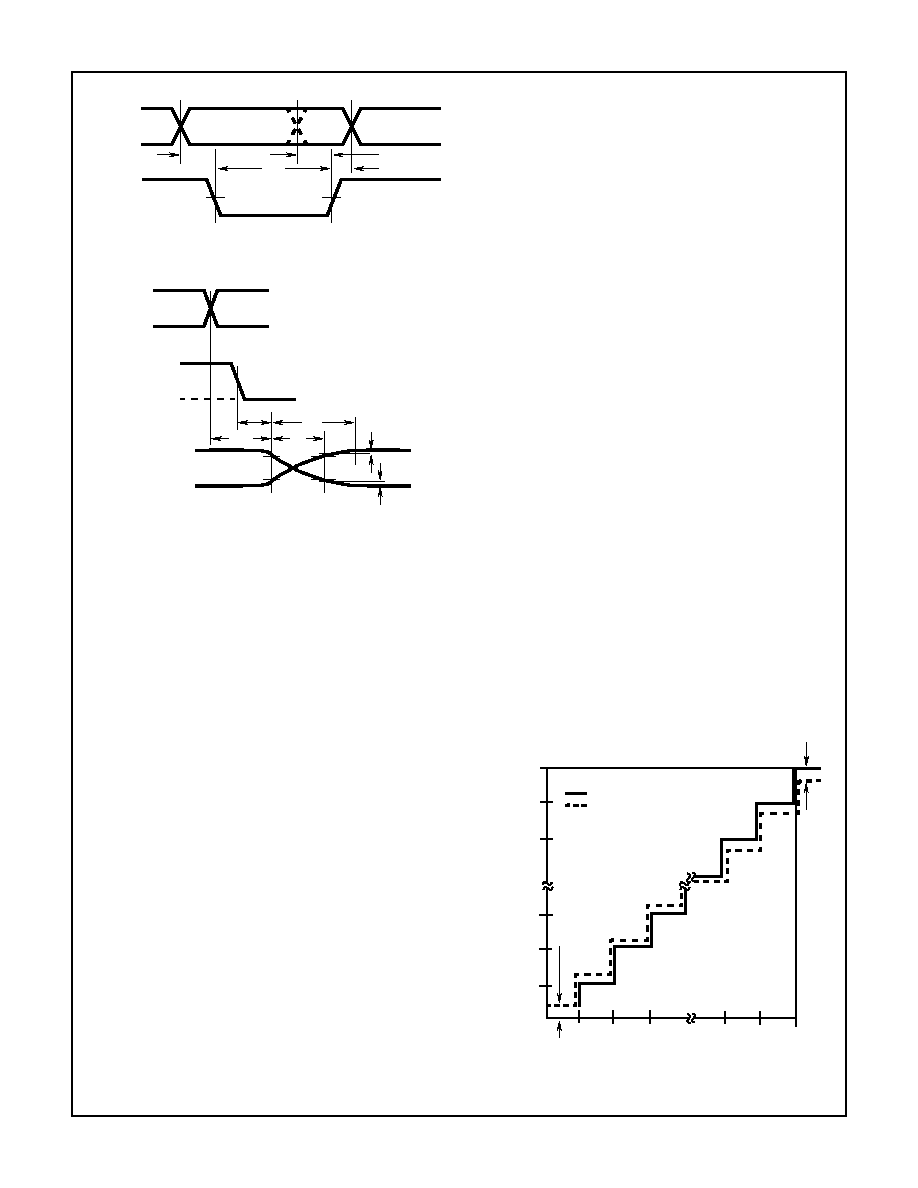
Latch Operation
Data is fed from input to output while LE is low: LE should be
tied low for non-clocked operation.
Non-clocked operation or changing data while LE is low is
not recommended for applications requiring low output
"glitch" energy: there is no guarantee of the simultaneous
changing of input data or the equal propagation delay of all
bits through the converter. Several parameters are given if
the converter is to be used in either of these modes: t
D2
gives the delay from the input changing to the output chang-
ing (10%), while t
SU2
and t
H
give the set up and hold times
(referred to LE rising edge) needed to latch data. See
Figures 1 and 2.
Clocked operation is needed for low "glitch" energy use.
Data must meet the given t
SU1
set up time to the LE falling
edge, and the t
H
hold time from the LE rising edge. The
delay to the output changing, t
D1
, is now referred to the LE
falling edge.
There is no need for a square wave LE clock; LE must only
meet the minimum t
W
pulse width for successful latch opera-
tion. Generally, output timing (desired accuracy of settling)
sets the upper limit of usable clock frequency.
Output Structure
The latches feed data to a row of high current CMOS drivers,
which in turn feed a modified R2R ladder network.
The "N" channel (pull down) transistor of each driver plus the
bottom "2R" resistor are returned to V
REF
- this is the (-) full-
scale reference. The "P" channel (pull up) transistor of each
driver is returned to V
REF
+, the (+) full-scale reference.
In unipolar operation, V
REF
- would typically be returned to
analog ground, but may be raised above ground (see specifi-
cations). There is substantial code dependent current that
flows from V
REF
+ to V
REF
- (see V
REF
+ input current in
specifications), so V
REF
- should have a low impedance path
to ground.
In bipolar operation, V
REF
- would be returned to a negative
voltage (the maximum voltage rating to V
DD
must be
observed). V
EE
, which supplies the gate potential for the
output drivers, must be returned to a point at least as nega-
tive as V
REF
-. Note that the maximum clocking speed
decreases when the bipolar mode is used.
Static Characteristics
The ideal 8-bit D/A would have an output equal to V
REF
- with
an input code of 00
HEX
(zero scale output), and an output
equal to 255/256 of V
REF
+ (referred to V
REF
-) with an input
code of FFHEX (full scale output). The difference between the
ideal and actual values of these two parameters are the OFF-
SET and GAIN errors, respectively; see Figure 3.
If the code into an 8-bit D/A is changed by 1 count, the output
should change by 1/255 (full scale output - zero scale output). A
deviation from this step size is a differential linearity error, see
Figure 4. Note that the error is expressed in fractions of the
ideal step size (usually called an LSB). Also note that if the (-)
differential linearity error is less (in absolute numbers) than 1
LSB, the device is monotonic. (The output will always increase
for increasing code or decrease for decreasing code).
If the code into an 8-bit D/A is at any value, say "N", the output
voltage should be N/255 of the full scale output (referred to the
zero scale output). Any deviation from that output is an integral
linearity error, usually expressed in LSBs. See Figure 4.
Note that OFFSET and GAIN errors do not affect integral
linearity, as the linearity is referenced to actual zero and full
scale outputs, not ideal. Absolute accuracy would have to
also take these errors into account.
INPUT DATA
LATCH
t
SU1
t
SU2
t
W
t
H
ENABLE
LATCHED
LATCHED
DATA
FEEDTHROUGH
FIGURE 1. DATA TO LATCH ENABLE TIMING
t
D1
t
D2
t
r
t
S
1
/
2
LSB
1
/
2
LSB
90%
10%
INPUT
LATCH
ENABLE
OUTPUT
VOLTAGE
DATA
FIGURE 2. DATA AND LATCH ENABLE TO OUTPUT TIMING
255/256
254/256
253/256
3/256
2/256
1/256
0
00
01
02
03
FD
FE
FF
= IDEAL TRANSFER CURVE
= ACTUAL TRANSFER CURVE
OFFSET
ERROR
(SHOWN +)
OUTPUT V
O
L
T
A
GE AS A FRA
CTION OF V
REF
+ - V
REF
-
GAIN ERROR
(SHOWN -)
INPUT CODE IN HEXADECIMAL (COMP = LOW)
FIGURE 3. D/A OFFSET AND GAIN ERROR
CA3338, CA3338A