 | –≠–ª–µ–∫—Ç—Ä–æ–Ω–Ω—ã–π –∫–æ–º–ø–æ–Ω–µ–Ω—Ç: CA3440 | –°–∫–∞—á–∞—Ç—å:  PDF PDF  ZIP ZIP |
3-146
Semiconductor
January 1999
Features
∑ High Input Resistance . . . . . . . . . . . . . . . . . . . 2T
(Typ)
∑ Standby Power at V+ = 5V . . . . . . . . . . . . . 300nW (Typ)
∑ Supply Current, BW, Slew Rate Programmable Using
External Resistor
∑ Input Current . . . . . . . . . . . . . . . . . . . . . . . . . 10pA (Typ)
∑ 5V to 15V Supply
∑ Output Drives Typical Bipolar Type Loads
Description
The CA3440 is an integrated circuit operational amplifier that
combines the advantages of MOS and bipolar transistors on
a single monolithic chip.
The CA3440 BiMOS op amp features gate protected PMOS
transistors in the input circuit to provide very high input
impedance, very low input currents (less than 10pA). This
device operates at total supply voltages from 5V to 15V and
can be operated over the temperature range from -55
o
C to
125
o
C. The virtues are programmability and very low
standby power consumption (300nW). This operational
amplifier is internally phase compensated to achieve stable
operation in the unity gain follower configuration. Terminals
are also provided for use in applications requiring input
offset voltage nulling. The use of PMOS in the input stage
results in common mode input voltage capability down to
0.5V below the negative supply terminals, an important
attribute for single supply applications. The output stage
uses MOS complementary source follower form which
permits moderate load driving capability (10k
) at very low
standby currents (50nA).
The CA3440 has the same 8 lead pinout as the "741" and
other industry standard op amps with two exceptions:
terminals one and five must be connected to the negative
supply or to a potentiometer if nulling is required. Terminal 8
must be programmed through an external resistor returned
to the negative supply.
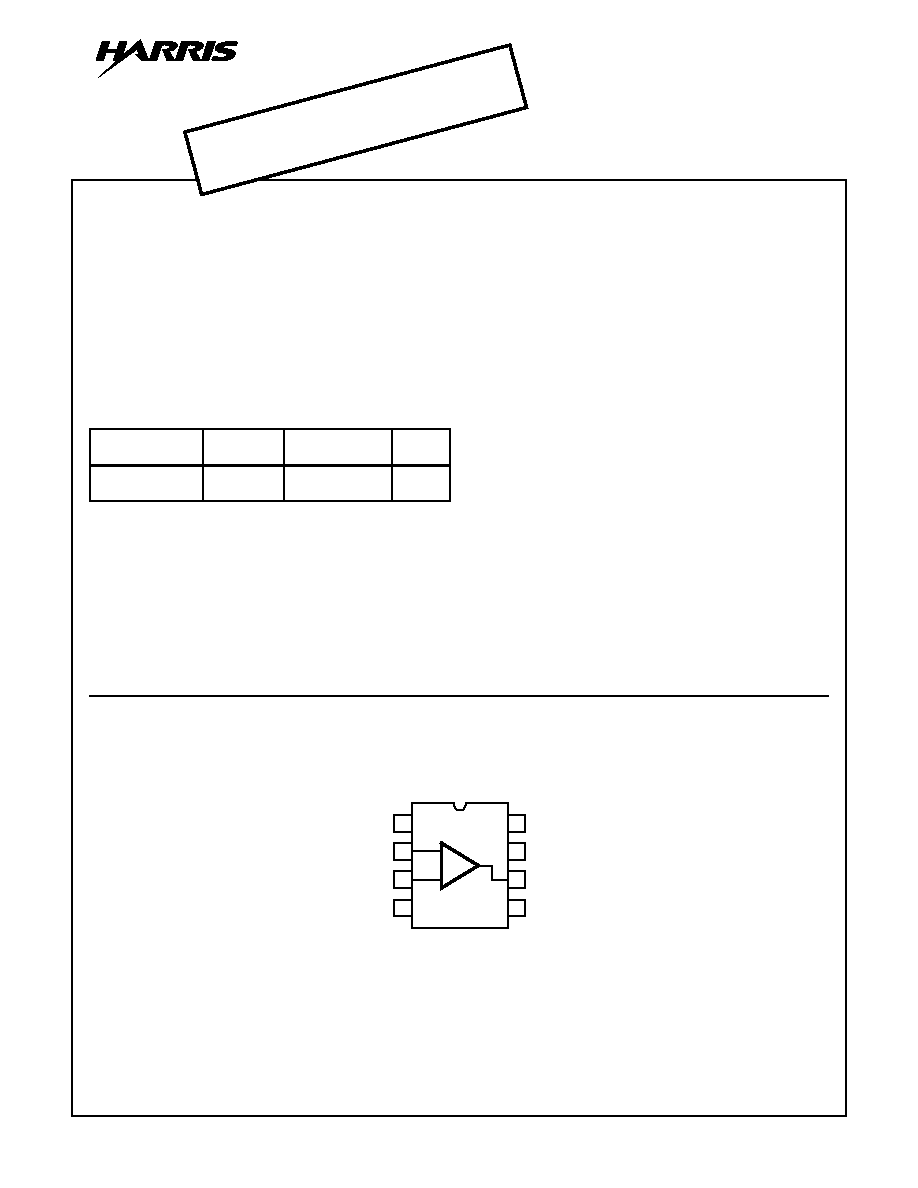
Pinout
CA3440
(SOIC)
TOP VIEW
Part Number Information
PART NUMBER
(BRAND)
TEMP.
RANGE (
o
C)
PACKAGE
PKG.
NO.
CA3440M
(3440)
-55 to 125
8 Ld SOIC
M8.15
1
2
3
4
8
7
6
5
V+
V-/OFFSET NULL
INV. INPUT
V-
NON-INV. INPUT
I
SET
OUTPUT
V-/OFFSET NULL
+
-
CAUTION: These devices are sensitive to electrostatic discharge. Users should follow proper IC Handling Procedures.
Copyright
©
Harris Corporation 1999
File Number
1318.5
CA3440
63kHz, Nanopower,
BiMOS Operational Amplifiers
OBSOLETE PR
ODUCT
POSSIBLE SUBSTITUTE PR
ODUCT
ICL7611, ICL7612

3-147
Absolute Maximum Ratings
Thermal Information
Supply Voltage (V+ to V-) . . . . . . . . . . . . . . . . . . . . . . . . . . . . . . 25V
Differential Input Voltage. . . . . . . . . . . . . . . . . . . . . . . . . . . . . . . . 9V
DC Input Voltage . . . . . . . . . . . . . . . . . . . . . . (V+ +8V) to (V- -0.5V)
Input Current. . . . . . . . . . . . . . . . . . . . . . . . . . . . . . . . . . . . . . . . 1mA
Output Short Circuit Duration (Note 1) . . . . . . . . . . . . . . . . Indefinite
Operating Conditions
Temperature Range . . . . . . . . . . . . . . . . . . . . . . . . -55
o
C to 125
o
C
Thermal Resistance (Typical, Note 2)
JA
(
o
C/W)
SOIC Package . . . . . . . . . . . . . . . . . . . . . . . . . . . . .
165
Maximum Junction Temperature (Die). . . . . . . . . . . . . . . . . . . . 175
o
C
Maximum Junction Temperature (Plastic Package) . . . . . . . . 150
o
C
Maximum Storage Temperature Range . . . . . . . . . .-65
o
C to 150
o
C
Maximum Lead Temperature (Soldering 10s) . . . . . . . . . . . . 300
o
C
(SOIC - Lead Tips Only)
CAUTION: Stresses above those listed in "Absolute Maximum Ratings" may cause permanent damage to the device. This is a stress only rating and operation
of the device at these or any other conditions above those indicated in the operational sections of this specification is not implied.
NOTES:
1. Short circuit may be applied to ground or to either supply.
2.
JA
is measured with the component mounted on an evaluation PC board in free air.
Electrical Specifications
Typical Values Intended Only for Design Guidance, V
SUPPLY
=
±
5V, R
SET
= 10M
, T
A
= 25
o
C
PARAMETER
SYMBOL
TEST CONDITIONS
CA3440
UNITS
Input Resistance
R
I
2
T
Input Capacitance
C
I
3.5
pF
Output Resistance
R
O
450
Equivalent Input
e
N
f = 1kHz
R
S
= 100
110
nV/
Hz
Noise Voltage
f = 10kHz
110
nV/
Hz
Short-Circuit Current
Source
I
OM
+
15
mA
To Opposite Supply
Sink
I
OM
-
4.5
mA
Gain Bandwidth Product
f
T
63
kHz
Slew Rate
SR
0.03
V/
µ
s
Transient Response
R
L
= 10k
, C
L
= 100pF
Rise Time
t
R
5.6
µ
s
Overshoot
OS
10
%
Electrical Specifications
For Equipment Design, At V
SUPPLY
=
±
5V; R
SET
= 10M
, T
A
= 25
o
C, Unless Otherwise Specified
PARAMETER
SYMBOL
TEST
CONDITIONS
CA3440
UNITS
MIN
TYP
MAX
Input Offset Voltage
|V
IO
|
-
5
10
mV
Input Offset Current
| I
IO
|
-
2.5
30
pA
Input Current
| I
I
|
-
10
50
pA
Large Signal Voltage Gain
A
OL
R
L
= 10k
10
100
-
kV/V
80
100
-
dB
Common Mode Rejection Ratio
CMRR
-
100
320
µ
V/V
70
80
-
dB
Common Mode Input Voltage Range
V
lCR
+
+3.5
+3.7
-
V
V
lCR
-
-5.0
-5.3
-
V
Power Supply Rejection Ratio
PSRR
-
32
320
µ
V/V
70
90
-
dB
Max Output Voltage
V
OM
+
+3
+3.2
-
V
V
OM
-
-3
-3.2
-
V
Supply Current
I+
-
10
17
µ
A
Device Dissipation
P
D
-
100
170
µ
W
Input Offset Voltage Temperature Drift
V
lO
/
T
-
4
-
µ
V/
o
C
CA3440
3-148
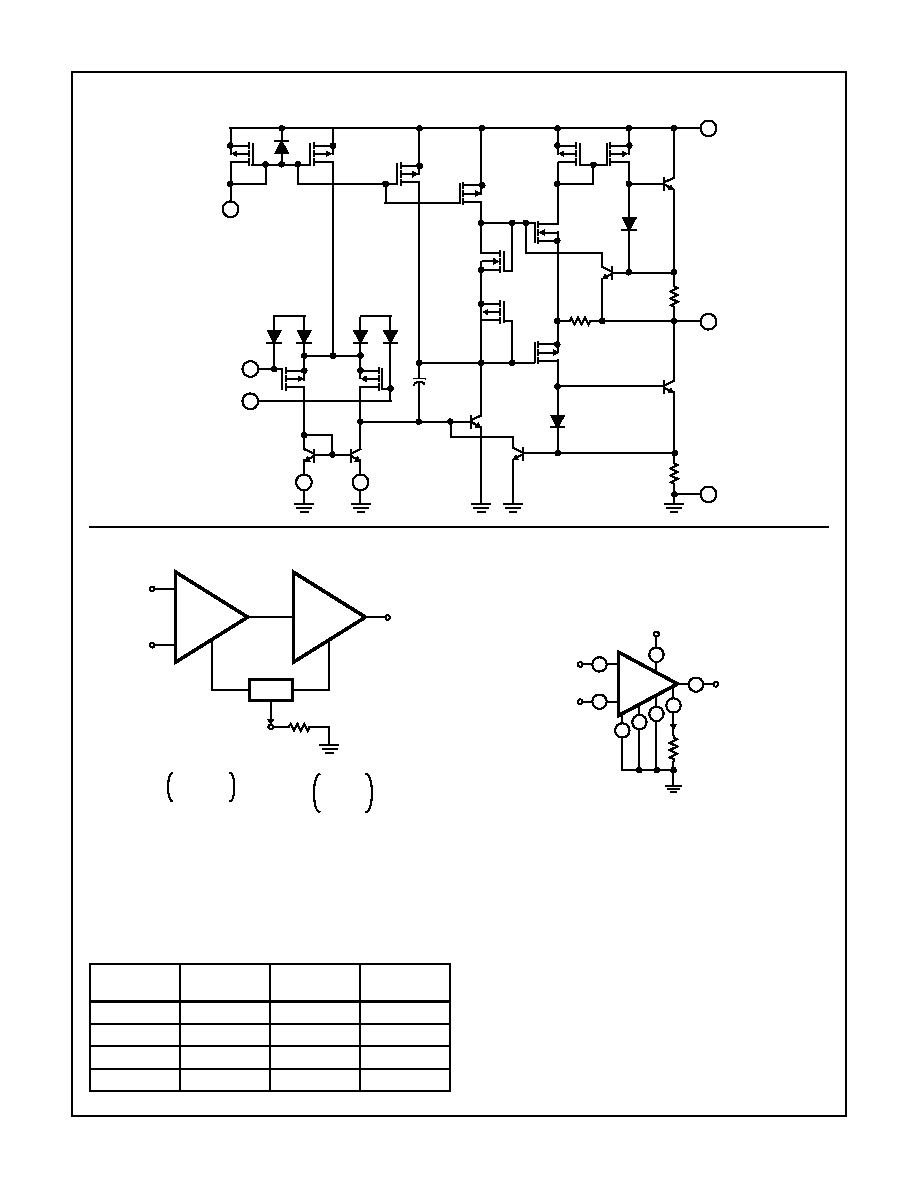
Schematic Diagram
Application Information
As R
SET
is increased, I
SET
and the standby power decrease
while the BW/SR also decrease.
Operating at a +5V single supply, the CA3440 exhibits the
following characteristics:
The CA3440 is pin compatible with the 741 except that pins
1 and 5 (typical negative nulling pins) must be connected
either directly to pin 4 or to a negative nulling potentiometer.
In addition, pin 8, the I
SET
terminal, must be returned to
either ground or -V via R
SET
.
Q
P1
Q
P2
D
1
D
2
Q
P3
Q
P4
D
4
D
3
Q
P5
Q
P6
Q
1
D
5
Q
N10
Q
N9
Q
P12
Q
P11
30pF
Q
P8
Q
P7
2
3
INVERTING
INPUT
NON-INVERTING
Q
3
Q
4
1
Q
5
Q
6
D
6
5
R
1
200
R
2
30
6
Q
7
R
3
30
4
8
7
V+
OUTPUT
V-
I
SET
Q
2
FIGURE 1. NANOPOWER OP AMP (SUPPLY CURRENT PRO-
GRAMMABLE USING R
SET
), 1pA TYPICAL INPUT
BIAS CURRENT, 4.0V TO 15V SUPPLY
FIGURE 2. NANOPOWER OP AMP (USABLE STANDBY
POWER vs PROGRAMMING RESISTOR R
SET
)
FET
INPUT
BIAS
FET/
BIPOLAR
OUTPUT
-
+
I
SET
R
SET
STAGE 1
HIGH GAIN
100dB
STAGE 2
BUFFER
LOW Z
OUTPUT
+5V
3
1
5
4
8
+
CA3440
-
2
7
6
I
SET
R
SET
R
SET
STANDBY
POWER
BW
SR
1M
250
µ
W
164kHz
0.17V/
µ
s
10M
25
µ
W
27kHz
0.017V/
µ
s
100M
2.5
µ
W
2.6kHz
0.0017V/
µ
s
1G
250nW
78kHz
0.00017V/
µ
s
CA3440
3-149
Typical Applications
FIGURE 3. HIGH INPUT IMPEDANCE AMPLIFIER
FIGURE 4. MICROPOWER BANDGAP REFERENCE
Typical Performance Curves
FIGURE 5. OUTPUT VOLTAGE SWING AND COMMON MODE
INPUT VOLTAGE RANGE vs SUPPLY VOLTAGE
FIGURE 6. SET CURRENT vs SUPPLY CURRENT
+9V
1
5
4
+
CA3440
-
2
7
6
8
22M
10M
OUTPUT
4.7M
2.2M
4.7M
2
µ
F
INPUT
500pF
R
IN
>20M
Standby Power = 90
µ
W
Gain = 20dB
BW: 20Hz to 3kHz
SR = 0.016V/
µ
s
+
3
1
5
4
+
CA3440
-
2
7
6
22M
+5V
2.35V
8
1.2M
12M
3
1.2M
7
10
3
13
6, 8
9, 11
1, 2
4, 5 DIODES
FROM CA3086
AT 200
µ
A
V
O
-
R
L
= 100k
10
SUPPLY VOLTAGE (V)
15
T
A
= 25
o
C
-2.0
V
O
+
V
ICR
-
V
ICR
+
5
0
-1.6
-1.2
-0.8
-0.4
0
0.4
0.8
1.2
1.6
2.0
0 = (V+ OR V-)
INPUT AND OUTPUT V
O
L
T
A
GE EXCURSIONS FR
OM
THE POSITIVE AND NEGA
TIVE SUPPL
Y V
O
L
T
A
GE (V)
V
S
=
±
5V
T
A
= 25
o
C
10,000
1000
100
10
SUPPLY CURRENT (nA)
1
10
1000
SET CURRENT (nA)
100
CA3440
3-150
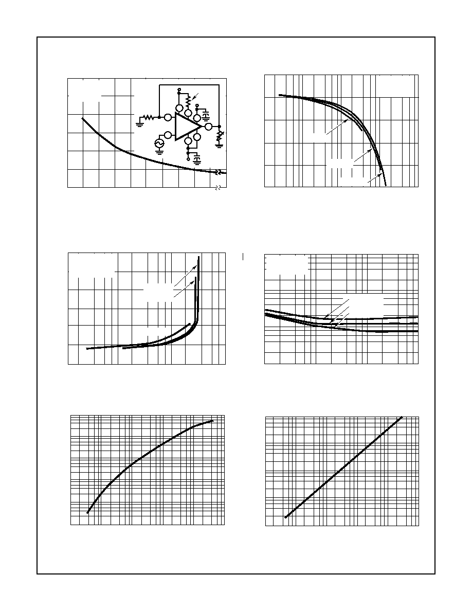
FIGURE 7. TOTAL HARMONIC DISTORTION vs LOAD
RESISTANCE
FIGURE 8. OUTPUT VOLTAGE vs SOURCING LOAD CURRENT
FIGURE 9. OUTPUT VOLTAGE vs SINKING LOAD CURRENT
FIGURE 10. INPUT NOISE VOLTAGE vs FREQUENCY
FIGURE 11. BANDWIDTH vs SET CURRENT
FIGURE 12. SLEW RATE vs SET CURRENT
Typical Performance Curves
(Continued)
14
LOAD RESISTANCE (k
)
6
0
12
10
8
4
2
0
2
4
6
8
10
12
T
O
T
AL HARMONIC DIST
OR
TION (%)
-5V
3
1
4
5
8
+
CA3440
-
2
7
6
0.1
µ
F
-5V
1kHz
1k
10M
+5V
0.1
µ
F
100
k
V
S
=
±
5V
T
A
= 25
o
C
I
SET
= 1
µ
A
16
18
V- = 0V
T
A
= 25
o
C
R
SET
= 1G
100
10
0.1
0.01
LOAD SOURCING CURRENT (mA)
OUTPUT V
O
L
T
A
GE FR
OM V+ RAIL (V)
1
V+ = 12V
-10
-8
-6
-4
-2
0
V+ = 10V
V+ = 5V
V- = -10V
V- = -12V
V+ = 0V
T
A
= 25
o
C
R
SET
= 1G
10
0.1
0.01
LOAD SINKING CURRENT (mA)
2
4
OUTPUT V
O
L
T
A
GE FR
OM V
-
RAIL (V)
1
6
8
10
12
0
V- = -5V
FREQUENCY (Hz)
10
4
10
3
10
2
10
1
10
1
10
2
10
3
10
4
EQ
UIV
ALENT INPUT NOISE V
O
L
T
A
GE (nV
Hz)
R
SET
= 10M
T
A
= 25
o
C
V
S
=
±
2.5V
V
S
=
±
5V
V
S
=
±
10V
SET CURRENT (nA)
10
5
10
4
10
3
1
10
1
10
2
10
4
10
5
B
AND
WIDTH (Hz)
10
2
10
1
10
6
10
3
SET CURRENT (nA)
10
5
10
4
10
3
1
10
2
10
4
10
5
SLEW RA
TE (
µ
V/
µ
s)
10
2
10
1
10
6
10
3
CA3440