 | –≠–ª–µ–∫—Ç—Ä–æ–Ω–Ω—ã–π –∫–æ–º–ø–æ–Ω–µ–Ω—Ç: CA3524E | –°–∫–∞—á–∞—Ç—å:  PDF PDF  ZIP ZIP |
1
CAUTION: These devices are sensitive to electrostatic discharge; follow proper IC Handling Procedures.
1-888-INTERSIL or 321-724-7143
|
Copyright
©
Intersil Corporation 2000
CA1524, CA2524
CA3524
Regulating Pulse Width Modulator
Description
The CA1524 and CA3524 are silicon monolithic integrated
circuits designed to provide all the control circuitry for use in
a broad range of switching regulator circuits.
The CA1524 and CA3524 have all the features of the indus-
try types SG1524, SG2524, and SG3524, respectively. A
block diagram of the CA1524 series is shown in Figure 1.
The circuit includes a zener voltage reference, transconduc-
tance error amplifier, precision R-C oscillator, pulse-width
modulator, pulse-steering flip-flop, dual alternating output
switches, and current-limiting and shutdown circuitry. This
device can be used for switching regulators of either polarity,
transformer-coupled dc-dc converter, transformerless volt-
age doublers, dc-ac power inverters, highly efficient variable
power supplies, and polarity converter, as well as other
power-control applications.
Ordering Information
PART
NUMBER
TEMPERATURE
RANGE
PACKAGE
CA1524E
-55
o
C to +125
o
C
16 Lead Plastic DIP
CA1524F
-55
o
C to +125
o
C
16 Lead CerDIP
CA2524E
0
o
C to +70
o
C
16 Lead Plastic DIP
CA2524F
0
o
C to +70
o
C
16 Lead CerDIP
CA3524E
0
o
C to +70
o
C
16 Lead Plastic DIP
CA3524F
0
o
C to +70
o
C
16 Lead CerDIP
Features
∑ Complete PWM Power Control Circuitry
∑ Separate Outputs for Single-Ended or Push-Pull
Operation
∑ Line and Load Regulation . . . . . . . . . . . . . . . 0.2% (Typ)
∑ Internal Reference Supply with 1% (Max) Oscillator
and Reference Voltage Variation Over Full
Temperature Range
∑ Standby Current of Less Than 10mA
∑ Frequency of Operation Beyond 100kHz
∑ Variable-Output Dead Time of 0.5
µ
s to 5
µ
s
∑ Low V
CE(sat)
Over the Temperature Range
Applications
∑ Positive and Negative Regulated Supplies
∑ Dual-Output Regulators
∑ Flyback Converters
∑ DC-DC Transformer-Coupled Regulating Converters
∑ Single-Ended DC-DC Converters
∑ Variable Power Supplies
File Number
1239.4
Pinout
CA1524, CA3524
(PDIP, CERDIP)
TOP VIEW
14
15
16
9
13
12
11
10
1
2
3
4
5
7
6
8
C
T
R
T
V
REF
EMITTER B
COLLECTOR B
COLLECTOR A
EMITTER A
SHUTDOWN
INV. INPUT
OSC OUT
GND
(-) C.L.
SENSE
(+) C.L.
SENSE
V+
COMPENSATION
AND COMPARATOR
NON-
INV. INPUT
October 2000
CA2524 IS AN OBSOLETE
PRODUCT
2
CA1524, CA2524, CA3524
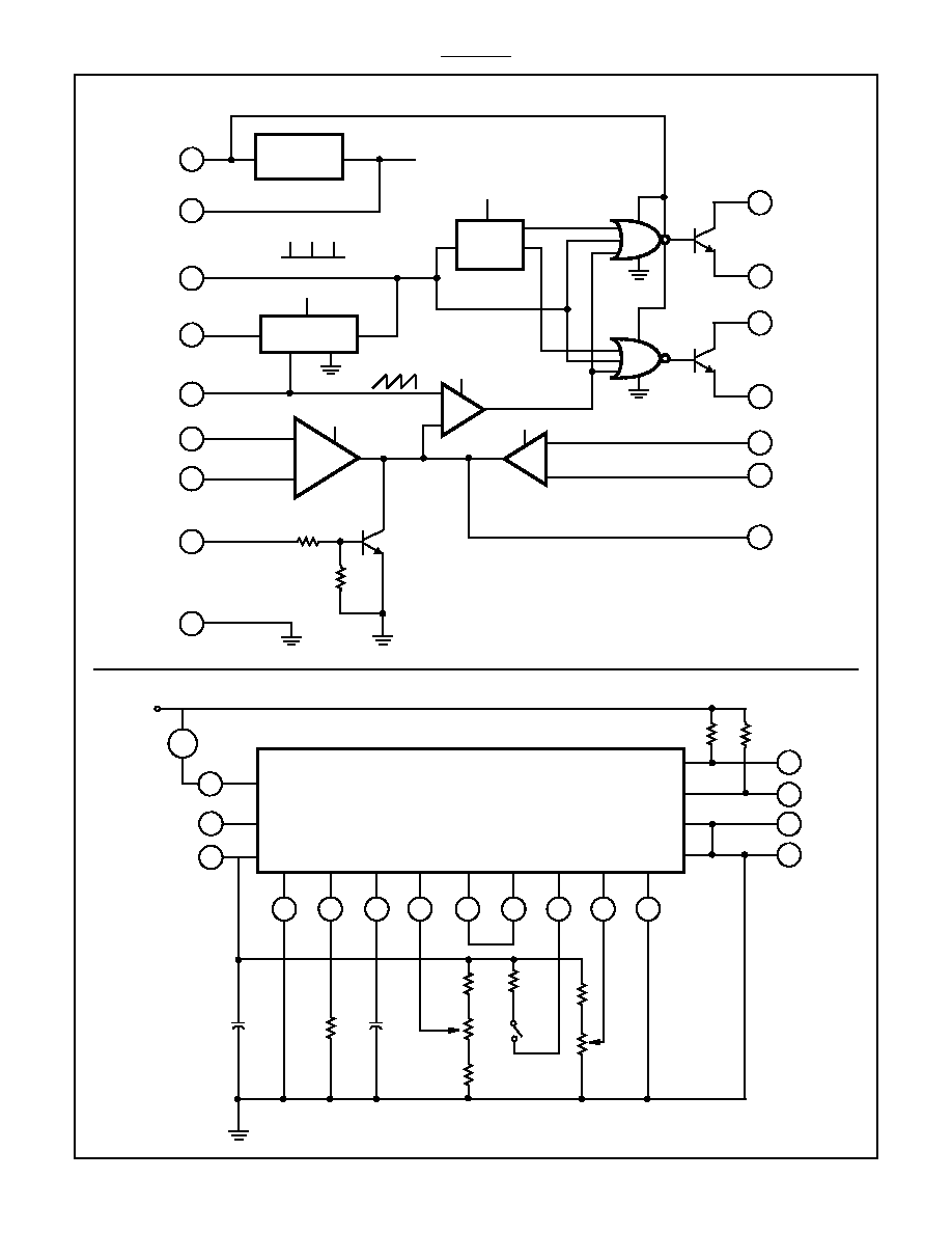
Functional Block Diagram
Test Circuit
REFERENCE
REGULATOR
5V
FLIP
OSCILLATOR
COMPARATOR
INV. INPUT
NON-INV.
INPUT
ERROR
AMP
SHUTDOWN
GND
16
15
3
6
7
1
2
10
8
FLOP
+5V
+5V TO ALL
INTERNAL CIRCUITS
+5V
-
+
+5V
+5V
C.L.
+5V
+
-
10k
1k
9
5
4
COMPENSATION AND COMPARATOR
- SENSE
+ SENSE
12
11
S
A
E
A
C
A
13
14
S
B
E
B
C
B
C
T
R
T
OSC OUT
V
REF
V+
12
13
11
14
5
4
10
9
1
2
7
6
8
16
15
3
ls
CA1524
V+
8 - 40V
0.1
µ
F
R
T
C
T
2k
10k
1k
10
k
2k
2k
2k
1W
2k
1W
OUT A
OUT B
3
Specifications CA1524, CA2524, CA3524
Absolute Maximum Ratings
Thermal Information
Input Voltage (Between V
IN
and GND Terminals). . . . . . . . . . . . 40V
Operating Voltage Range (V
IN
to GND) . . . . . . . . . . . . . . . . 8 to 40V
Output Current Each Output:
(Terminal 11, 12 or 13, 14) . . . . . . . . . . . . . . . . . . . . . . . . . 100mA
Output Current (Reference Regulator) . . . . . . . . . . . . . . . . . . . 50mA
Oscillator Charging Current . . . . . . . . . . . . . . . . . . . . . . . . . . . . 5mA
Thermal Resistance
JA
Plastic DIP Package . . . . . . . . . . . . . . . . . . . . . . . .
100
o
C/W
Device Dissipation
Up to T
A
= +25
o
C . . . . . . . . . . . . . . . . . . . . . . . . . . . . . . . . . 1.25W
Above T
A
= +25
o
C . . . . . . . . . . . . . . .Derate Linearly at 10mW/
o
C
Operating Temperature Range . . . . . . . . . . . . . . . . -55
o
C to +125
o
C
Storage Temperature Range . . . . . . . . . . . . . . . . . . -65
o
C to +150
o
C
Lead Temperature (During Soldering)
At distance 1/16
±
in. (1.59mm
±
0.79mm)
from case for 10s Max . . . . . . . . . . . . . . . . . . . . . . . . . . . . +265
o
C
CAUTION: Stresses above those listed in "Absolute Maximum Ratings" may cause permanent damage to the device. This is a stress only rating and operation
of the device at these or any other conditions above those indicated in the operational sections of this specification is not implied.
Electrical Specifications
T
A
= -55
0
C to +125
o
C for CA1524, 0
o
C to +70
o
C for the CA2524 and CA3524; V+ = 20V and
f = 20kHz, Unless Otherwise Stated.
PARAMETER
TEST CONDITIONS
CA1524, CA2524
CA3524
UNITS
MIN
TYP
MAX
MIN
TYP
MAX
REFERENCE SECTION
Output Voltage
4.8
5
5.2
4.6
5
5.4
V
Line Regulation
V+ = 8 to 40V
-
10
20
-
10
30
mV
Load Regulation
I
L
= 0 to 20mA
-
20
50
-
20
50
mV
Ripple Rejection
f = 120Hz, T
A
= 25
o
C
-
66
-
-
66
-
db
Short Circuit Current Limit
V
REF
= 0, T
A
= 25
o
C
-
100
-
-
100
-
mA
Temperature Stability
Over Operating Temperature
Range
-
0.3
1
-
0.3
1
%
Long Term Stability
T
A
= 25
o
C
-
20
-
-
20
-
mV/khr
OSCILLATOR SECTION
Maximum Frequency
C
T
= 0.001
µ
F, R
T
= 2K
-
300
-
-
300
-
kHz
Initial Accuracy
R
T
and C
T
Constant
-
5
-
-
5
-
%
Voltage Stability
V+ = 8 to 40V, T
A
= 25
o
C
-
-
1
-
-
1
%
Temperature Stability
Over Operating Temperature
Range
-
-
2
-
-
2
%
Output Amplitude
Terminal 3, T
A
= 25
o
C
-
3.5
-
-
3.5
-
V
Output Pulse Width (Pin 3)
C
T
= 0.01
µ
F, T
A
= 25
o
C
-
0.5
-
-
0.5
-
µ
s
Ramp Voltage Low (Note 1)
Pin 7
-
0.6
-
-
0.6
-
V
Ramp Voltage High (Note 1)
Pin 7
-
3.5
-
-
3.5
-
V
Capacitor Charging Current Range
Pin 7 (5-2 V
BE
)/R
T
0.03
-
2
0.03
-
2
mA
Timing Resistance Range
Pin 6
1.8
-
120
1.8
-
120
k
Charging Capacitor Range
Pin 7
0.001
-
0.1
0.001
-
0.1
µ
F
Dead Time Expansion Capacitor on
Pin 3 (when a small osc. cap is used)
Pin 3
100
-
1000
100
-
1000
pF
ERROR AMPLIFIER SECTION
Input Offset Voltage
V
CM
= 2.5V
-
0.5
5
-
2
10
mV
Input Bias Current
V
CM
= 2.5V
-
1
10
-
1
10
µ
A
Open Loop Voltage Gain
72
80
-
60
80
-
dB
Common Mode Voltage
T
A
= 25
o
C
1.8
-
3.4
1.8
-
3.4
V
Common Mode Rejection Ratio
T
A
= 25
o
C
-
70
-
-
70
-
dB
Small Signal Bandwidth
A
V
= 0dB, T
A
= 25
o
C
-
3
-
-
3
-
MHz
4
Specifications CA1524, CA2524, CA3524
Output Voltage
T
A
= 25
o
C
0.5
-
3.8
0.5
-
3.8
V
Amplifier Pole
-
250
-
-
250
-
Hz
Pin 9 Shutdown Current
External Sink
-
200
-
-
200
-
µ
A
COMPARATOR SECTION
Duty Cycle
% Each Output On
0
-
45
0
-
45
%
Input Threshold
Zero Duty Cycle
-
1
-
-
1
-
V
Input Threshold
Max. Duty Cycle
-
3.5
-
-
3.5
-
V
Input Bias Current
-
1
-
-
1
-
µ
A
CURRENT LIMITING SECTION
Sense Voltage for 25% Output Duty
Cycle
Terminal 9 = 2V with Error
Amplifier Set for Max Out,
T
A
= 25
o
C
190
200
210
180
200
220
mV
Sense Voltage T.C.
-
0.2
-
-
0.2
-
mV/
o
C
Common Mode Voltage
-1
-
+1
-1
-
+1
V
Rolloff Pole of R51 C3 + Q64
-
300
-
-
300
-
Hz
OUTPUT SECTION (EACH OUTUT)
Collector-Emitter Voltage
40
-
-
40
-
-
V
Collector Leakage Current
V
CE
= 40V
-
0.1
50
-
0.1
50
µ
A
Saturation Voltage
V+ = 40V, I
C
= 50mA
-
0.8
2
-
0.8
2
V
Emitter Output Voltage
V+ = 20V
17
18
-
17
18
-
V
Rise Time
R
C
= 2K
, T
A
= 25
o
C
-
0.2
-
-
0.2
-
µ
s
Fall Time
R
C
= 2K
, T
A
= 25
o
C
-
0.1
-
-
0.1
-
µ
s
Total Standby Current: (Note 2) I
S
V+ = 40V
-
4
10
-
4
10
mA
NOTES:
1. Ramp voltage at Pin 7
where
t = OSC period in microseconds
t
R
T
C
T
with C
T
in microfarads and R
T
in ohms.
Output frequency at each output transistor is half OSC frequency when each output is used separately and is equal to the OSC frequency
when each output is connected in parallel.
2. Excluding oscillator charging current, error and current limit dividers, and with outputs open.
Electrical Specifications
T
A
= -55
0
C to +125
o
C for CA1524, 0
o
C to +70
o
C for the CA2524 and CA3524; V+ = 20V and
f = 20kHz, Unless Otherwise Stated. (Continued)
PARAMETER
TEST CONDITIONS
CA1524, CA2524
CA3524
UNITS
MIN
TYP
MAX
MIN
TYP
MAX
High
Low
t

5
CA1524, CA2524, CA3524
Schematic Diagram
2
1
3
7
6
8
Q1
R1
500
R5
1K
R7
1K
Q2
Q7
Q13
Q6
Q3 Q4
R2
2.7K
RC
10K
R3
6.3K
Q10
Q11
D2
D1
Q9
C1
20pF
R4
500
R6
500
Q5
Q12
RB
4.8K
RA
5.3K
QA
OSC SECTION
Q42
Q43
Q44
Q47
Q48
Q49
Q50
Q45
Q46
R39
1K
R41
24K
R40
560
R42
19.8K
Q51
Q52
R45
25K
R44
1.8K
R43
7.4K
Q53
Q54
Q55
R46
3.3K
OSC.
OUT
Q59
Q60
Q61
Q56 Q57
INV.
IN
ERROR
AMP
NON-INV.
INPUT
Q58
Q62
R47
1K
R48
2K
J
K
L
F
G
H
I
C
D
E
Q24
Q22
Q20
R15
25K
C2
20pF
N
+
P
10K
1.9K
RD
Q19
R14
450
Q14
Q15
R8
8.4K
R9
500
R10
1K
Q17
Q18
R11
500
R12
10K
Q16
R13
6
15 V
IN
C4
PULSE
STEERING
FLIP-FLOP
B
A
R16
16.2K
R19
18.7
K
R17
18.7
K
R18
18.7
K
R18
18.7
K
Q21
Q23
16
V
REF
+5V
GND
R
T
C
T
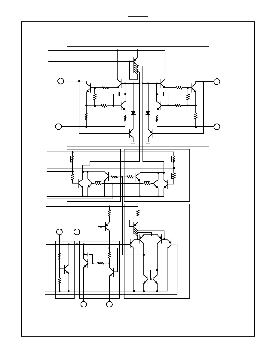
6
CA1524, CA2524, CA3524
Schematic Diagram
(Continued)
12
11
COLL. A
EMIT A
13
COLL. B
14
EMIT B
10
9
5
4
A
B
OUTPUT A
Q34
Q36
Q35
R33
200
R32
1K
R34
500
CA
1pF
R31
4.7
RE
500
Q33
OUTPUT B
Q40
Q37
Q38
D3
D4
Q39
RF
500
R38
4.7
Q41
R35
500
R37
1K
R36
200
CB
1pF
C
D
E
R21
43.3K
R25
5K
R24
5K
Q26
Q27
R23
8.7K
F
G
H
I
R26
5K
Q29
R27
5K
Q30
Q31
R30
43.3K
R28
8.7K
NOR
NOR
R52
1.96K
R54
1.96K
Q65
Q67
J
COMP
R49
1K
R50
10K
Q63
Q64
Q66
CURRENT
LIMIT
SECTION
R51
10K
R53
1.8K
C3
45pF
(-) C.L.
SENSE
Q68
Q71
Q70
Q68
Q73
Q72
K
L
COMPARATOR
(+) C.L.
SENSE
7
CA1524, CA2524, CA3524
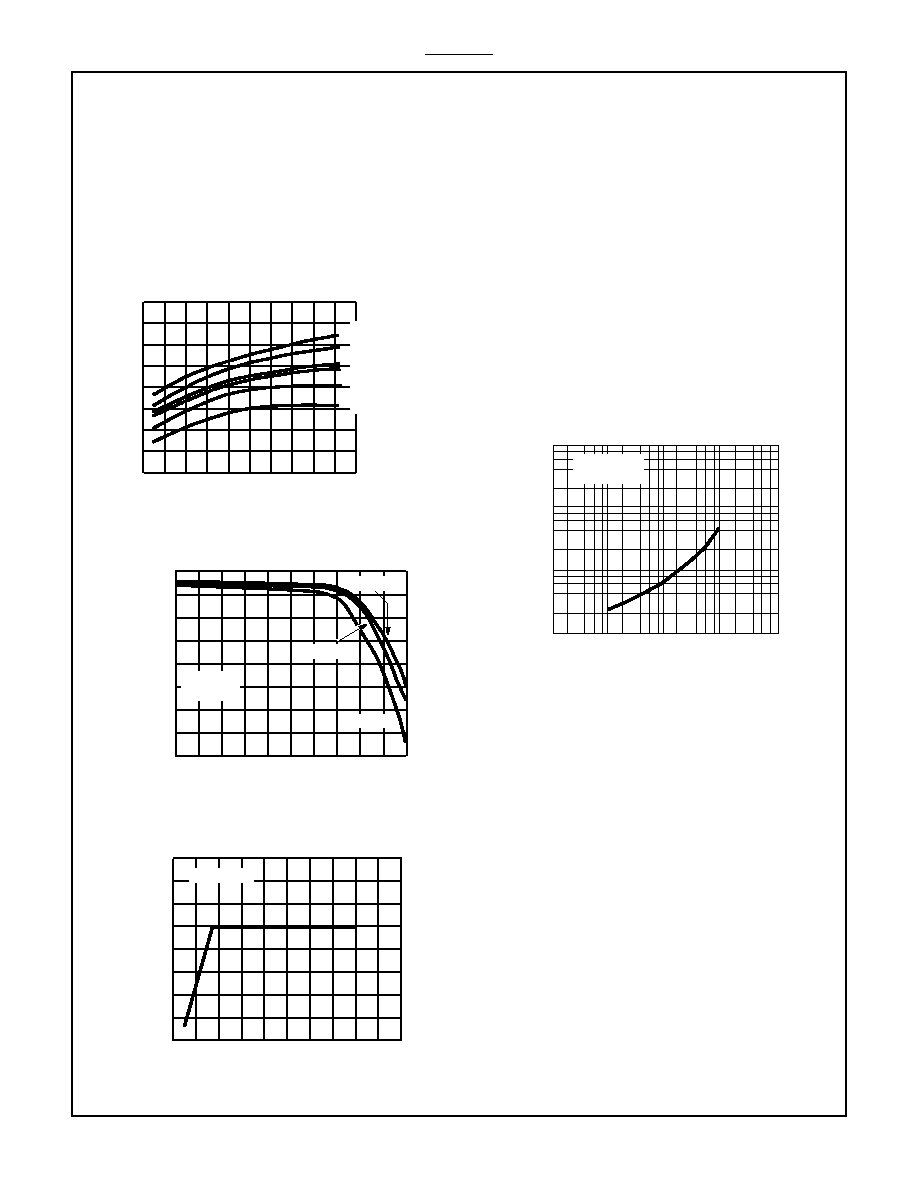
Circuit Description
Voltage Reference Section
The CAl524 series contains an internal series voltage regu-
lator employing a zener reference to provide a nominal 5-volt
output, which is used to bias all internal timing and control
circuitry. The output of this regulator is available at terminal
l6 and is capable of supplying up to 50mA output current.
Figure 1 shows the temperature variation of the reference
voltage with supply voltages of 8V to 40V and load currents
up to 20mA. Load regulation and line regulation curves are
shown in Figures 2 and 3, respectively.
FIGURE 1. TYPICAL REFERENCE VOLTAGE AS A FUNCTION
OF AMBIENT TEMPERATURE
FIGURE 2. TYPICAL REFERENCE VOLTAGE AS A FUNCTION
OF REFERENCE OUTPUT CURRENT
FIGURE 3. TYPICAL REFERENCE VOLTAGE AS A FUNCTION
OF SUPPLY VOLTAGE
5.02
5.00
4.98
4.96
REFERENCE V
O
L
T
A
GE (V)
-60 -40 -20
0
20
40
60
80 100 120 140
AMBIENT TEMPERATURE (
o
C)
V+ = 40V, I
L
= 0mA
V+ = 20V, I
L
= 0mA
V+ = 40V, I
L
= 20mA
V+ = 8V, I
L
= 0mA
V+ = 20V, I
L
= 20mA
V+ = 8V, I
L
= 20mA
REFERENCE V
O
L
T
A
GE (V)
5.1
4.9
4.7
4.5
4.3
4.1
3.9
3.7
3.5
0
8
16
24
32
40
48
56
64
72
80
REFERENCE OUTPUT CURRENT (mA)
TA = +25oC
V+ = 20V
V+ = 40V
V+ = 20V
V+ = 8V
6
5
4
3
2
1
0
0
7
8
REFERENCE V
O
L
T
A
GE (V)
10
20
30
40
SUPPLY VOLTAGE, V+ (V)
TA = +25oC
Osclllator Section
Transistors Q42, Q43 and Q44, in conjunction with an
external resistor R
T
, establishes a constant charging current
into an external capacitor C
T
to provide a linear ramp voltage
at terminal 7. The ramp voltage has a value that ranges from
0.6V to 3.5V and is used as the reference for the comparator
in the device. The charging current is equal to (5-2V
BE
)/R
T
or
approximately 3.6/R
T
and should be kept within the range of
30pA to 2mA by varying R
T
. The discharge time of C
T
deter-
mines the pulse width of the oscillator output pulse at termi-
nal 3. This pulse has a practical range of 0.5
µ
s to 5
µ
s for a
capacitor range of 0.001 to 0.1
µ
F. The pulse has two internal
uses: as a dead-time control of blanking pulse to the output
stages to assure that both outputs cannot be on simulta-
neously and as a trigger pulse to the internal flip-flop which
controls the switching of the output between the two output
channels. The output dead-time relationship is shown in Fig-
ure 4. Pulse widths less than 0.5
µ
s may allow false trigger-
ing of one output by removing the blanking pulse prior to a
stable state in the flip-flop.
FIGURE 4. TYPICAL OUTPUT STAGE DEAD TIME AS A
FUNCTION OF TIMING CAPACITOR VALUE
If a small value of C
T
must be used, the pulse width can be
further expanded by the addition of a shunt capacitor in the
order of 100pF but no greater than 1000pF, from terminal 3
to ground. When the oscillator output pulse is used as a sync
input to an oscilloscope, the cable and input capacitances
may increase the pulse width slightly. A 2-K
resistor at
terminal 3 will usually provide sufficient decoupling of the
cable. The upper limit of the pulse width is determined by the
maximum duty cycle acceptable.
The oscillator period is determined by R
T
and C
T
, with an
approximate value of t = R
T
C
T
, where R
T
is in ohms, C
T
is in
µ
F, and t is in
µ
s. Excess lead lengths, which produce stray
capacitances, should be avoided in connecting R
T
and C
T
to
their respective terminals. Figure 5 provides curves for
selecting these values for a wide range of oscillator periods.
For series regulator applications, the two outputs can be
connected in parallel for an effective 0-90% duty cycle with
the output stage frequency the same as the oscillator
frequency. Since the outputs are separate, push-pull and
flyback applications are possible. The flip-flop divides the
frequency such that the duty cycle of each output is 0-45%
and the overall frequency is half that of the oscillator. Curves
OUTPUT DEAD TIME (
µ
s)
100
10
1.0
0.1
0.0001
0.001
0.01
0.1
1.0
TIMING CAPACITOR, C
T
(
µ
F)
T
A
= +25
o
C
V+ = 8V - 40V
8
CA1524, CA2524, CA3524
of the output duty cycle as a function of the voltage at
terminal 9 are shown in Figure 7. To synchronize two or
more CAl524's, one must be designated as master, with R
T
C
T
set for the correct period. Each of the remaining units
(slaves) must have a C
T
of 1/2 the value used in the master
and approximately a 1010 longer R
T
C
T
period than the mas-
ter. Connecting terminal 3 together on all units assures that
the master output pulse, which occurs first and has a wider
pulse width, will reset the slave units.
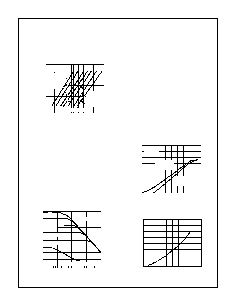
FIGURE 5. TYPICAL OSCILLATOR PERIOD AS A FUNCTION
OF R
T
AND C
T
Error AmplIfIer Section
The error amplifier consists of a differential pair (Q56,Q57)
with an active load (Q61 and Q62) forming a differential
transconductance amplifier. Since Q61 is driven by a
constant current source, Q62, the output impedance R
OUT
,
terminal 9, is very high (
5M
).
The gain is:
A
V
= g
m
R = 8 l
C
R/2KT = 10
4
,
Since R
OUT
is extremely high, the gain can be easily
reduced from a nominal 10
4
(80dB) by the addition of an
external shunt resistor from terminal 9 to ground as shown in
Figure 6.
FIGURE 6. OPEN-LOOP ERROR AMPLIFIER RESPONSE
CHARACTERISTICS.
where R =
R
OUT
R
L
, R
L
=
, A
V
10
4
R
OUT
+
R
L
TIMING RESIST
ANCE, R
T
(
)
10
5
10
4
10
3
1
10
10
2
10
3
10
4
OSCILLATOR PERIOD, t (
µ
s)
T
A
= +25
o
C
V+ = 8V - 40V
C
T
= 0.01
µ
F
C
T
= 0.002
µ
F
C
T
= 0.005
µ
F
C
T
= 0.001
µ
F
C
T
= 0.02
µ
F
C
T
= 0.05
µ
F
C
T
= 0.1
µ
F
V
O
L
T
A
GE GAIN (dB)
80
70
60
50
40
0
o
90
o
PHASE ANGLE (DEGREES)
R
L
=
R
L
= 3M
R
L
= 1M
R
L
= 300k
R
L
=100k
OPEN LOOP PHASE
OPEN LOOP GAIN
10
10
2
10
3
10
4
10
5
50
FREQUENCY (Hz)
The output amplifier terminal is also used to compensate the
system for ac stability. The frequency response and phase
shift curves are shown in Figure 7. The uncompensated
amplifier has a single pole at approximately 250Hz and a
unity gain cross-over at 3MHz.
Since most output filter designs introduce one or more
additional poles at a lower frequency, the best network to
stabilize the system is a series RC combination at terminal9
to ground. This network should be designed to introduce a
zero to cancel out one of the output filter poles. A good start-
ing point to determine the external poles is a 1000-pF
capacitor and a variable series 50-K
potentiometer from
terminal 9 to ground. The compensation point is also a
convenient place to insert any programming signal to
override the error amplifier. internal shutdown and current
limiting are also connected at terminal 9. Any external circuit
that can sink 200
µ
A can pull this point to ground and shut off
both output drivers.
While feedback is normally applied around the entire regula-
tor, the error amplifier can be used with conventional
operational amplifier feedback and will be stable in either the
inverting or non-inverting mode. Input common-mode limits
must be observed; if not, output signal inversion may result.
The internal 5V reference can be used for conventional regu-
lator applications if divided as shown in Figure 8. If the error
amplifier is connected as a unity gain amplifier, a fixed duty
cycle application results.
FIGURE 7. TYPICAL DUTY CYCLE AS A FUNCTION OF
COMPARATOR VOLTAGE (AT TERMINAL 9).
FIGURE 8. TYPICAL OUTPUT SATURATION VOLTAGE AS A
FUNCTION OF AMBIENT TEMPERATURE.
OUTPUT DUTY CYCLE (%)
48
40
32
24
16
8
0
COMPARATOR VOLTAGE (V)
0
0.4 0.8 1.2 1.6
2
2.4 2.8 3.2 3.6
4
T
A
= +25
o
C
V+ = 20V
C
T
= 2700pF
R
T
= 6.19k
f
OSC
= 60kHz
C
T
=1000pF
R
T
= 5k
f
OSC
= 20kHz
1.1
1.0
0.9
0.8
0.7
-75 -50 -25
0
25
50
75 100 125 150 175
OUTPUT SA
TURA
TION V
O
L
T
A
GE (V)
AMBIENT TEMPERATURE (
o
C)
9
CA1524, CA2524, CA3524
Output Section
The CA1524 series outputs are two identical n-p-n
transistors with both collectors and emitters uncommitted.
Each output transistor has antisaturation circuitry that
enables a fast transient response for the wide range of
oscillator frequencies. Current limiting of the output section
is set at 100mA for each output and 100mA total if both
outputs are paralleled. Having both emitters and collectors
available provides the versatility to drive either n-p-n or p-n-p
external transistors. Curves of the output saturation voltage
as a function of temperature and output current are shown in
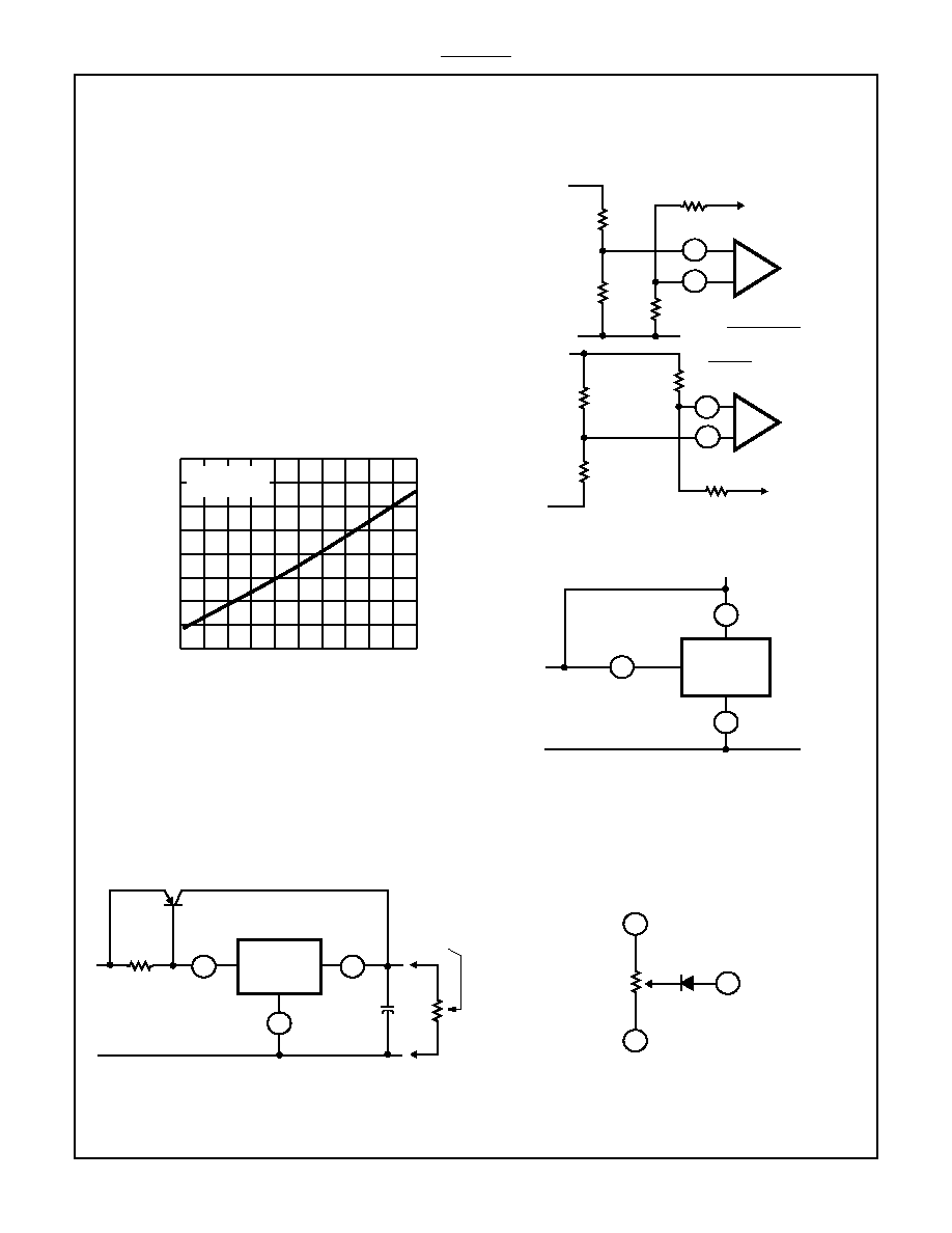
Figures 8 and 9, respectively. There are a number of output
configurations possible in the application of the CA1524 to
voltage regulator circuits which fall into three basic
classifications:
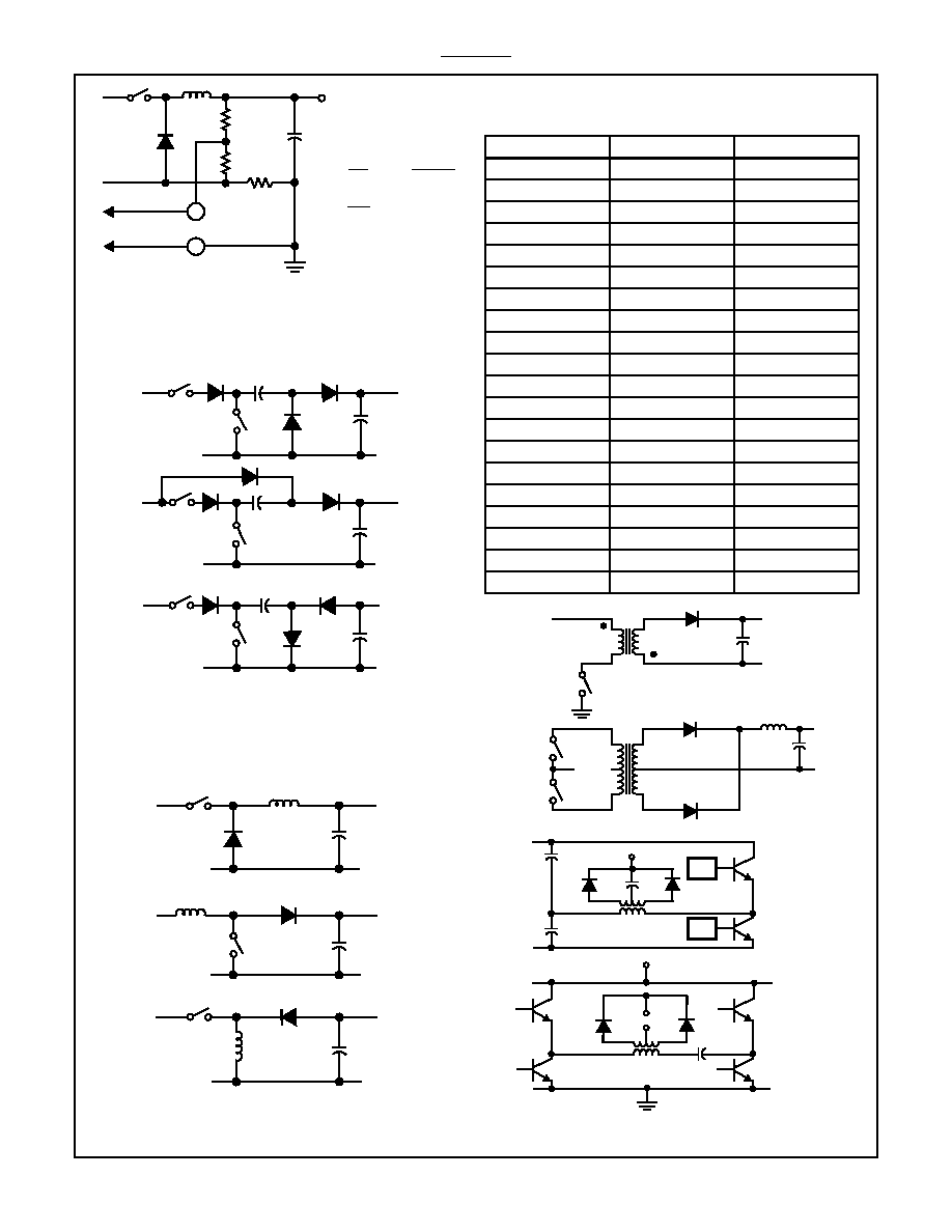
1. Capacitor-diode coupled voltage multipliers
2. Inductor-capacitor single-ended circuits
3. Transformer-coupled circuits
FIGURE 9. TYPICAL OUTPUT SATURATION VOLTAGE AS A
FUNCTION OF OUTPUT CURRENT
Device Application Suggestions
For higher currents, the circuit of Figure 10 may be used with
an external p-n-p transistor and bias resistor. The internal
regulator may be bypassed for operation from a fixed 5V
supply by connecting both terminals 15 and 16 to the input
voltage, which must not exceed 6V.
FIGURE 10. CIRCUIT FOR EXPANDING THE REFERENCE
CURRENT CAPABILITY
The internal 5V reference can be used for conventional regu-
lator applications if divided as shown in Figure 11. If the error
amplifier is connected as a unity gain amplifier, a fixed duty
cycle application results.
FIGURE 11. ERROR AMPLIFIER BIASING CIRCUITS
FIGURE 12. CIRCUIT TO ALLOW EXTERNAL BYPASS OF THE
REFERENCE REGULATION
To provide an expansion of the dead time without loading the
oscillator, the circuit of Figure 13 may be used.
FIGURE 13. CIRCUIT FOR EXPANSION OF DEAD TIME, WITH-
OUT USING A CAPACITOR ON PIN 3 OR WHEN A
LOW VALUE OSCILLATOR CAPACITOR IS USED
OUTPUT SA
TURA
TION V
O
L
T
A
GE (V)
2.0
1.5
1.0
0.5
0
0
20
40
60
80
100
OUTPUT CURRENT, I
L
(mA)
T
A
= +25
o
C
V+ = 8V to 40V
CA1524
REFERENCE
SECTION
15
16
8
V+
I
L
TO I
A
DEPENDING
ON CHOICE
FOR Q1
GND
100
Q1
10
µ
F
+
-
V
REF
V
REF
2
1
R2
5K
5K
R1
-
+
-
+
2
1
R2
V
REF
GND
GND
5K
5K
NEGATIVE
OUTPUT
VOLTAGES
POSITIVE
OUTPUT
VOLTAGES
V
O
2.5V (R1 + R2)
R1
R1R2
R1 + R2
= 2.5KW
R1
CA1524
REFERENCE
SECTION
15
16
8
V+ CANNOT
EXCEED 6V
V
T
V
REF
NOTE: V+ Should Be in the 5V Range
And Must Not Exceed 6V
8
16
9
5K
10
CA1524, CA2524, CA3524
FIGURE 14. FOLDBACK CURRENT-LIMITING CIRCUIT USED
TO
REDUCE
POWER
DISSIPATION
UNDER
SHORTED OUTPUT CONDITIONS
FIGURE 15. CAPACITOR-DIODE COUPLED VOLTAGE
MULTIPLIER OUTPUT STAGES
FIGURE 16. SINGLE-ENDED INDUCTOR CIRCUITS WHERE THE
TWO OUTPUTS OF THE 1524 ARE CONNECTED IN
PARALLEL
FIGURE 17. TRANSFORMER-COUPLED OUTPUTS
5
4
S
A
//S
B
R1
R2
RS
SENSE
V
O
= 5V
I
MAX
=
I
R
S
V
TH
+
V
O
R
2
R1 + R2
(
)
I
SC
=
V
TH
R
S
WHERE
V
TH
= 200mV
+
-
V+
V+
V+
S
A
S
A
S
A
S
B
S
B
S
B
D1
D1
D1
V+ > V
O
V+ < V
O
| V+ | > | V
O
|
+V
O
+V
O
-V
O
NOTE: Diode D1 Is Necessary To Prevent Reverse
Emitter-Base Breakdown of Transistor Switch S
A
.
V+
V+
V+
S
A
/S
B
S
A
/S
B
S
A
/S
B
+V
O
+V
O
-V
O
| V+ | < | V
O
|
V+ < V
O
V+ > V
O
TABLE 1. INPUT vs. OUTPUT VOLTAGE, AND FEEDBACK
RESISTOR VALUES FOR I
L
= 40mA (FOR CAPACI-
TOR-DIODE OUTPUT CIRCUIT IN FIGURE 18)
V
O
(V)
R
2
(K
)
V+ (Min.) (V)
-0.5
6
8
-2.5
10
9
-3
11
10
-4
13
11
-5
15
12
-6
17
13
-7
19
14
-8
21
15
-9
23
16
-10
25
17
-11
27
18
-12
29
19
-13
31
20
-14
33
21
-15
35
22
-16
37
23
-17
39
24
-18
41
25
-19
43
26
-20
45
27
S
A-B
V+
V
O
V+
S
A
S
B
PUSH-PULL
FLYBACK
V
O
V
O
FULL BRIDGE
V+
+
-
V
O
+
-
V+
S
A
S
B
Q1
Q2
CAN BE S
A
OR
S
A
CAN DRIVEQ1
CAN BE S
B
OR
S
B
CAN DRIVEQ2
11
CA1524, CA2524, CA3524
Applications
(Note 1)
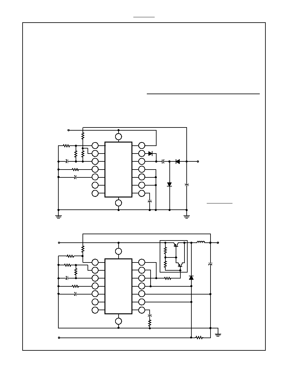
A capacitor-diode output filter is used in Figure 19 to convert
+15V
DC
to -5V
DC
at output currents up to 50mA. Since the
output transistors have built-in current limiting, no additional
current limiting is needed. Table 1 gives the required
minimum input voltage and feedback resistor values, R2, for
an output voltage.
Capacitor-Diode Output Circuit
A capacitor-diode output filter is used in Figure18 to convert
+15V
DC
to -5V
DC
at output currents up to 50mA. Since the
output transistors have built-in current limiting, no additional
current limiting is needed. Table 1 gives the required
minimum input voltage and feedback resistor values, R2, for
an output voltage range of -0.5V to -20V with an output
current of 40mA.
Single-Ended Switching Regulator
The CA1524 in the circuit of Figure 19 has both output
stages connected in parallel to produce an effective 0% -
90% duty cycle. Transistor Q1 is pulsed on and off by these
output stages. Regulation is achieved from the feedback
provided by R1 and R2 to the error amplifier which adjusts
the on-time of the output transistors according to the load
current being drawn. Various output voltages can be
obtained by adjusting R1 and R2. The use of an output
inductor requires an R-C phase compensation network to
stabilize the system. Current limiting is set at 1.9 amperes by
the sense resistor R3.
NOTE:
1. For additional information on the application of this device and a
further explanation of the circuits below, see Intersil Application
Note AN6915 "Application of the CA1524 series PWM lC".
FIGURE 18. CAPACITOR-DIODE OUTPUT CIRCUIT
FIGURE 19. SINGLE-ENDED LC SWITCHING REGULATOR CIRCUIT
1
CA3524
1
1
2
1
16
1
6
1
7
1
3
1
10
1
12
1
11
1
13
1
14
1
4
1
5
1
9
1
8
1
6
+15V
V+
5K
2K
0.1
µ
F
5K
R1
5K
0.01
µ
F
0.01
µ
F
R2
15K
IN4001
IN4001
20
µ
F
IN4001
50
µ
F
-5V
20mA
R1 = 5K
R2 =
R1 ( | V
O
| + 2.5)
(V
REF
- 2.5)
1
CA3524
1
1
2
1
16
1
6
1
7
1
3
1
10
1
12
1
11
1
13
1
14
1
4
1
5
1
9
1
8
1
15
+28V
V+
5K
3K
0.1
µ
F
5K
0.02
µ
F
0.001
µ
F
R2
5K
RURD410
V-
50K
0.1
500
µ
F
0.9mH
Q1
2N6388
2K
+5V IA
R1
5K
12
CA1524, CA2524, CA3524
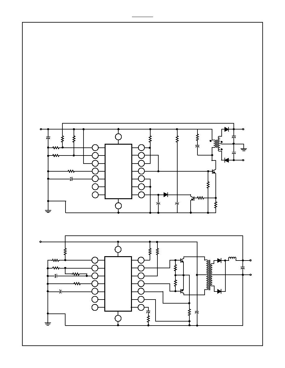
Flyback Converter
Figure 20 shows a flyback converter circuit for generating a
dual 15V output at 20mA from a 5V regulated line.
Reference voltage is provided by the input and the internal
reference generator is unused. Current limiting in this circuit
is accomplished by sensing current in the primary line and
resetting the soft-start circuit.
Push-Pull Converter
The output stages of the CA1524 provide the drive for
transistors Q1 and Q2 in the push-pull application of Figure
21. Since the internal flip-flop divides the oscillator frequency
by two, the oscillator must be set at twice the output
frequency. Current limiting for this circuit is done in the
primary of transformer T1 so that the pulse width will be
reduced if transformer saturation should occur.
Low-Frequency Pulse Generator
Figure 22 shows the CA1524 being used as a low-frequency
pulse generator. Since all components (error amplifier,
oscillator, oscillator reference regulator, output transistor
drivers) are on the lC, a regulated 5-V (or 2.5-V) pulse of 0%
- 45% (or 0% - 90%) on time is possible over a frequency
range of 150 to 500Hz. Switch S1 is used to go from a 5-V
output pulse (S1 closed) to a 2.5-V output pulse (S1 open)
with a duty cycle range of 0% to 45%. The output frequency
will be roughly half of the oscillator frequency when the
output transistors are not connected in parallel (75Hz to
250Hz, respectively). Switch S2 will allow both output stages
to be paralleled for an effective duty cycle of 0%-90% with
the output frequency range from 150 to 500Hz. The
frequency is adjusted by R1; R2 controls duty cycle.
FIGURE 20. FLYBACK CONVERTER CIRCUIT
FIGURE 21. PUSH-PULL TRANSFORMER-COUPLED CONVERTER
1
CA3524
1
1
2
1
16
1
6
1
7
1
3
1
10
1
12
1
11
1
13
1
14
1
4
1
5
1
9
1
8
1
15
+5V
V+
25K
2K
100
µ
F
0.02
µ
F
0.001
µ
F
620
300
1
RURD620
5K
4.7
µ
F
+
+
1M
510
+15V
-15V
50
µ
F
50
µ
F
50T
50T
20T
200
0.1
µ
F
2N6290
CORE: FEROX CUBE
2213P - A250 - 387
OR EQUIVALENT
2N2102
IN914
5K
5K
RURD620
1
1
1
2
1
16
1
6
1
7
1
3
1
10
1
12
1
11
1
13
1
14
1
4
1
5
1
9
1
8
1
15
+28V
V+
5K
2K
0.1
µ
F
20K
1K
1500
µ
F
1K
5K
5K
5K
0.01
µ
F
1W
0.001
µ
F
+
100
µ
F
0.1
µ
F
5T
5T
20T
20T
+
5V
5A
1mH
1K
2N6292
2N6292
1K
1W
RURD620
RURD620
13
CA1524, CA2524, CA3524
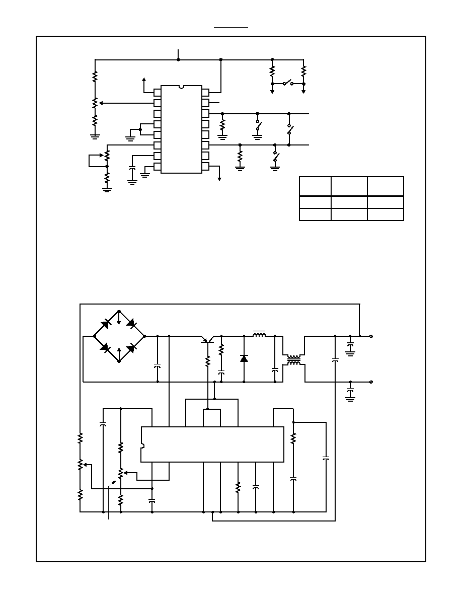
The Variable Switcher
The circuit diagram of the CA1524, used as a variable output
voltage power supply is shown in Figure 23. By connecting
the two output transistors in parallel, the duty cycle is
doubled, i.e., 0% - 90%. As the reference voltage level is
varied, the feedback voltage will track that level and cause
the output voltage to change according to the change in
reference voltage.
FIGURE 22. LOW-FREQUENCY PULSE GENERATOR
14
15
16
9
13
12
11
10
1
2
3
4
5
7
6
8
TO PIN 9
V
REFERENCE
+5
R1
50K
20K
FREQUENCY
ADJUSTMENT
0.1
µ
F
SILVER
MICA
2K
2K
R2
10K
DUTY CYCLE
ADJUSTMENT
V
+
= 9V
1.5K
1.5K
CA3524
1
/
2
S1
1
/
2
S1
1
/
2
S2
OUTPUT 1A
OUTPUT 2A
1.1K
1.1K
1
/
2
S2
TO PIN 12
OUTPUT 1
TO PIN 1
TO PIN 13
OUTPUT 2
SWITCH
OUTPUT
PULSES
DUTY
CYCLE
S1
0V - 5V
0% - 45%
S2
-
0% - 90%
FIGURE 23. THE CA1524 USED AS A 0-5A, 7-30 V LABORATORY SUPPLY
L1
20mH
D2
D4
D3
D1
AC
IN
5100
µ
F
100V
D1-D4 - A15A
V
DC
36
R1
1K
1W
Q1
2N6385
(PNP DARLINGTON)
R2
1.5
10W
0.01
µ
F
D5
C3
10000
µ
F
100V
BIFILAR
WINDING
L2
50mH
V
OUT
C4
0.1
µ
F
7V - 30V
0A - 3A
RETURN
C5
25
µ
F
NON-POLAR
C6
25
µ
F
NON-POLAR
R10
16K
C11
0.01
µ
F
C10
1100pF
SILVER
MICA
C9
3300
pF
1%
R9
15K
1%
C8
0.1
µ
F
R8
2K
R7
10K
R6
2K
R4
5K
R5
2K
R3
10K
C7
0.1
µ
F
16
15
14
13
12
11
10
9
1
2
3
4
5
6
7
8
CA1524
VOLTAGE
CONTROL
f
OSC
= 20KHz
RURD410

14
CA1524, CA2524, CA3524
Digital Readout Scale
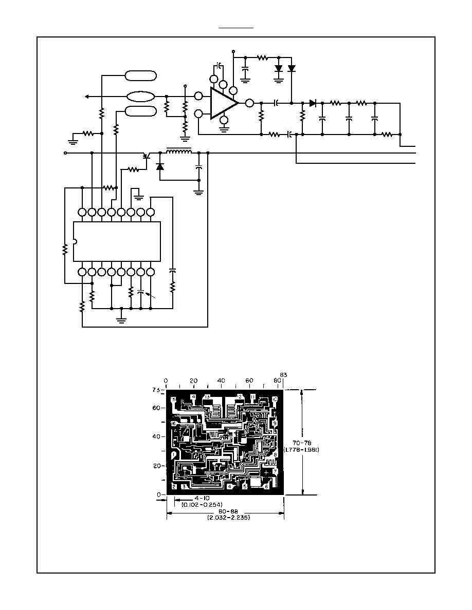
The CA1524 can be used as the driving source for an
electronic scale application. The circuit shown in Figures 24
and 25 uses half (Q2) of the CA1524 output in a low-voltage
switching regulator (2.2V) application to drive the LED's
displaying the weight. The remaining output stage (Q1) is
used as a driver for the sampling plates PL1 and PL2. Since
the CA1524 contains a 5V internal regulator and a wide
operating range of 8V to 40V, a single 9V battery can power
the total system. The two plates, PL1 and PL2, are driven
with opposite phase signals (frequency held constant but
duty cycle may change) from the pulse-width modulator lC
(CA1524). The sensor, S, is located between the two plates.
Plates PL1, S and PL2 form an effective capacitance bridge-
type divider network. As plate S is moved according to the
object's weight, a change in capacitance is noted between
PL1, S and PL2. This change is reflected as a voltage to the
ac amplifier (CA3160). At the null position the signals from
PL1 and PL2 as detected by S are equal in amplitude, but
opposite in phase. As S is driven by the scale mechanism
down toward PL2, the signal at S becomes greater. The
CA3160 ac amplifier provides a buffer for the small signal
change noted at S. The output of the CA3160 is converted to
a dc voltage by a peak-to-peak detector. A peak-to-peak
detector is needed, since the duty cycle of the sampled
waveform is subject to change. The detector output is filtered
further and displayed via the CA3161E and CA3162E digital
readout system, indicating the weight on the scale.
FIGURE 24. BASIC DIGITAL READOUT SCALE
FIGURE 25. SCHEMATIC DIAGRAM OF DIGITAL READOUT SCALE (CONT'D)
OSCILLATOR
20KHz
(PART OF CA1524)
PL1
PL2
S
AC
AMP
CA3130
COUPLED TO
MECHANICAL
SCALE MECHANISM
PEAK TO PEAK
DETECTOR
LOW PASS
FILTER
DISPLAY DRIVE
(PART OF CA1524)
DIGITAL METER
AND DISPLAY
FULL SCALE
NO WEIGHT
DC
VOLTAGE
13
12
11
10
9
15
14
16
15
2
6
1
7
2
1
13
7
CA3161E
CA3162E
8
3
4
3
5
16
MSD
NSD
LSD
+5V
COMMON-
ANODE LED
DISPLAYS
11
10
POWER 2N2907
OR EQUIVALENT
BCD
OUTPUTS
DIGIT
DRIVERS
8
12 14
9
0.1
µ
F
10K
0.27
µ
F
ZERO
ADJUSTMENT
50K
2.5V
A
B
C
HIGH
LOW
INPUTS:
GAIN
ADJUSTMENT
(NOTE 1)
NOTE:
1. FAIRCHILD FND507 OR EQUIVALENT
15
CA1524, CA2524, CA3524
FIGURE 26. SCHEMATIC DIAGRAM OF DIGITAL READOUT SCALE
DIMENSIONS AND PAD LAYOUT FOR CA3524RH CHIP
6
4
2
3
PL1
S
PL2
9V
30K
39K
430K
100
M
22M
1
8
7
CA3160
+
-
200pF
9V
10K
100
µ
F
68K
6.2K
10K
0.1
µ
F
910K
910K
2
µ
F
0.47
2
µ
F
µ
F
300K
A
B
C
10
µ
F
2.5V
22M
14
15
16
13 12 11 10
9
8
7
6
5
4
3
2
1
4.7K
200
2N4037
9V
TO SCALE
MECHANISM
125
µ
H
470
µ
F
CA1524
24K
0.01
µ
F
4.7K
4.7K
6.2K
4700pF
4.7K
5V
NOTE: Dimensions in parentheses are in millimeters and are de-
rived from the basic inch dimensions as indicated. Grid graduations
are in mils (10
-3
inch). The layout represents a chip when it is part of
the wafer. When the wafer is cut into chips, the cleavage angles are
57
o
instead of 90
o
with respect to the face of the chip. Therefore, the
isolated chip is actually 7 mils (0.17mm) larger in both dimensions.

16
All Intersil semiconductor products are manufactured, assembled and tested under ISO9000 quality systems certification.
Intersil products are sold by description only. Intersil Corporation reserves the right to make changes in circuit design and/or specifications at any time without notice.
Accordingly, the reader is cautioned to verify that data sheets are current before placing orders. Information furnished by Intersil is believed to be accurate and reli-
able. However, no responsibility is assumed by Intersil or its subsidiaries for its use; nor for any infringements of patents or other rights of third parties which may
result from its use. No license is granted by implication or otherwise under any patent or patent rights of Intersil or its subsidiaries.
For information regarding Intersil Corporation and its products, see web site http://www.intersil.com
File Number