 | –≠–ª–µ–∫—Ç—Ä–æ–Ω–Ω—ã–π –∫–æ–º–ø–æ–Ω–µ–Ω—Ç: CA5130A | –°–∫–∞—á–∞—Ç—å:  PDF PDF  ZIP ZIP |
1
TM
File Number
1923.6
CAUTION: These devices are sensitive to electrostatic discharge; follow proper IC Handling Procedures.
1-888-INTERSIL or 321-724-7143
|
Intersil and Design is a trademark of Intersil Corporation.
|
Copyright
©
Intersil Corporation 2000
CA5130, CA5130A
15MHz, BiMOS Microprocessor
Operational Amplifiers with MOSFET
Input/CMOS Output
CA5130A and CA5130 are integrated circuit operational
amplifiers that combine the advantage of both CMOS and
bipolar transistors on a monolithic chip. They are designed
and guaranteed to operate in microprocessors or logic
systems that use +5V supplies.
Gate protected P-Channel MOSFET (PMOS) transistors are
used in the input circuit to provide very high input
impedance, very low input current, and exceptional speed
performance. The use of PMOS field effect transistors in the
input stage results in common mode input voltage capability
down to 0.5V below the negative supply terminal, an
important attribute in single supply applications.
A complementary symmetry MOS (CMOS) transistor-pair,
capable of swinging the output voltage to within 10mV of
either supply voltage terminal (at very high values of load
impedance), is employed as the output circuit.
The CA5130 Series circuits operate at supply voltages ranging
from 4V to 16V, or
±
2V to
±
8V when using split supplies. They
can be phase compensated with a single external capacitor,
and have terminals for adjustment of offset voltage for
applications requiring offset null capability. Terminal provisions
are also made to permit strobing of the output stage.
The CA5130A, CA5130 have guaranteed specifications for
5V operation over the full military temperature range of
-55
o
C to 125
o
C.
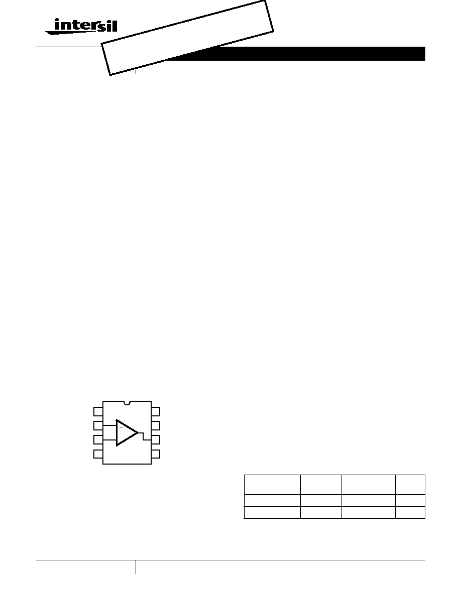
Pinout
CA5130 (PDIP)
TOP VIEW
Features
∑ MOSFET Input Stage
- Very High Z
l
. . . . . . . . . . . . . 1.5T
(1.5 x 10
12
) (Typ)
- Very Low l
l
. . . . . . . . . . . . . 5pA (Typ) at 15V Operation
2pA (Typ) at 5V Operation
∑ Ideal for Single Supply Applications
∑ Common Mode Input Voltage Range Includes
Negative Supply Rail; Input Terminals Can Be Swung
0.5V Below Negative Supply Rail
∑ CMOS Output Stage Permits Signal Swing to Either (or Both)
Supply Rails
∑ CA5130A, CA5130 Have Full Military Temperature Range
Guaranteed Specifications for V+ = 5V
∑ CA5130A, CA5130 Are Guaranteed to Operate Down to
V+ = 4.5V for A
OL
∑ CA5130A, CA5130 Are Guaranteed to Operate at
±
7.5V
CA3130A, CA3130 Specifications
Applications
∑ Ground Referenced Single Supply Amplifiers
∑ Fast Sample-Hold Amplifiers
∑ Long Duration Timers/Monostables
∑ High Input lmpedance Comparators (Ideal Interface with
Digital CMOS)
∑ High lnput Impedance Wideband Amplifiers
∑ Voltage Followers (e.g., Follower for Single-Supply
D/A Converter)
∑ Voltage Regulators (Permits Control of Output Voltage
Down to 0V)
∑ Peak Detectors
∑ Single Supply Full Wave Precision Rectifiers
∑ Photo Diode Sensor Amplifiers
∑ 5V Logic Systems
∑ Microprocessor Interface
1
2
3
4
8
7
6
5
V+
OFFSET NULL
INV. INPUT
V-
NON-INV. INPUT
STROBE
OUTPUT
OFFSET NULL
+
Part Number Information
PART NUMBER
(BRAND)
TEMP.
RANGE (
o
C)
PACKAGE
PKG.
NO.
CA5130AE
-55 to 125
8 Ld PDIP
E8.3
CA5130E
-55 to 125
8 Ld PDIP
E8.3
Data Sheet
March 2000
[ /Title
()
/Sub-
ject ()
/Autho
r ()
/Key-
words
()
/Cre-
ator ()
/DOCI
NFO
pdf-
mark
[
/Page-
Mode
/Use-
Out-
lines
/DOC-
VIEW
pdf-
mark
OBSOLETE PR
ODUCT
POSSIBLE SUBSTITUTE PR
ODUCT
CA3130
2
Absolute Maximum Ratings
Thermal Information
Supply Voltage (V+ to V-). . . . . . . . . . . . . . . . . . . . . . . . . . . . . . .16V
DC Input Voltage . . . . . . . . . . . . . . . . . . . . . . (V+ +8V) to (V- -0.5V)
Differential Input Voltage . . . . . . . . . . . . . . . . . . . . . . . . . . . . . . . .8V
Input Terminal Current . . . . . . . . . . . . . . . . . . . . . . . . . . . . . . . . 1mA
Output Short-Circuit Duration (Note 1) . . . . . . . . . . . . . . . Indefinite
Operating Conditions
Temperature Range . . . . . . . . . . . . . . . . . . . . . . . . . -55
o
C to 125
o
C
Thermal Resistance (Typical, Note 2)
JA
(
o
C/W)
JC
(
o
C/W)
PDIP Package . . . . . . . . . . . . . . . . . . .
120
N/A
Maximum Junction Temperature (Plastic Package) . . . . . . . 150
o
C
Maximum Storage Temperature Range . . . . . . . . . . -65
o
C to 150
o
C
Maximum Lead Temperature (Soldering 10s) . . . . . . . . . . . . 300
o
C
CAUTION: Stresses above those listed in "Absolute Maximum Ratings" may cause permanent damage to the device. This is a stress only rating and operation of the
device at these or any other conditions above those indicated in the operational sections of this specification is not implied.
NOTES:
1. Short circuit may be applied to ground or to either supply.
2.
JA
is measured with the component mounted on an evaluation PC board in free air.
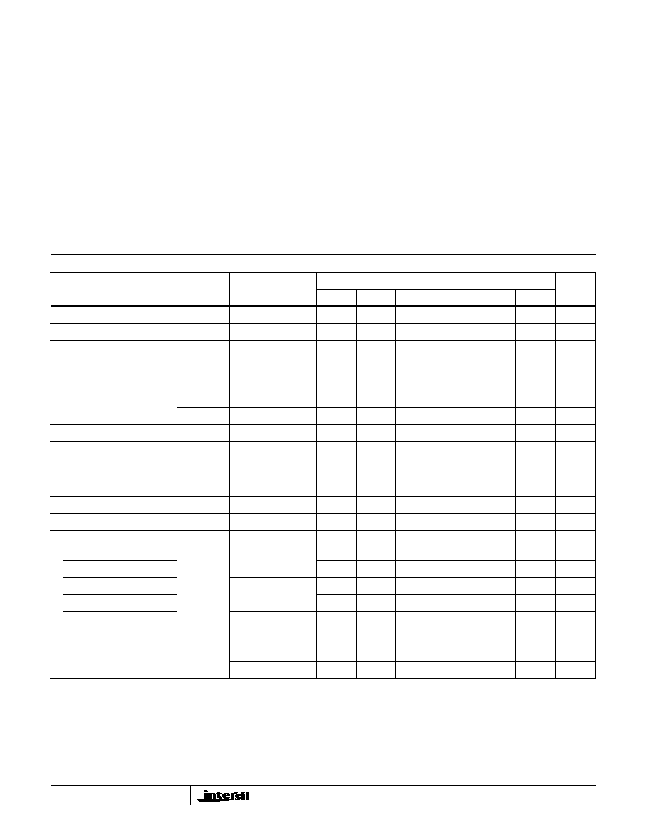
Electrical Specifications
T
A
= 25
o
C, V+ = 5V, V- = 0V, Unless Otherwise Specified
PARAMETER
SYMBOL
TEST
CONDITIONS
CA5130
CA5130A
UNITS
MIN
TYP
MAX
MIN
TYP
MAX
Input Offset Voltage
V
IO
V
O
= 2.5V
-
2
10
-
1.5
4
mV
Input Offset Current
I
IO
V
O
= 2.5V
-
0.1
10
-
0.1
5
pA
Input Current
I
I
V
O
= 2.5V
-
2
15
-
2
10
pA
Common Mode Rejection Ratio
CMRR
V
CM
= 0V to 1V
70
85
-
75
87
-
dB
V
CM
= 0V to 2.5V
60
69
-
60
69
-
dB
Input Common Mode Voltage
Range
V
ICR
+
2.5
2.8
-
2.5
2.8
-
V
V
ICR
-
-
-0.5
0
-
-0.5
0
V
Power Supply Rejection Ratio
PSRR
+ = 1V;
- = 1V
55
73
-
60
75
-
dB
Large Signal Voltage Gain
(Note 3)
A
OL
V
O
= 0.1V to 4.1V
R
L
=
95
105
-
100
105
-
dB
V
O
= 0.1V to 3.6V
R
L
= 10k
85
95
-
90
97
-
dB
Source Current
I
SOURCE
V
O
= 0V
1.0
2.6
4.0
1.0
3.1
4.0
mA
Sink Current
I
SINK
V
O
= 5V
1.0
1.7
4.0
1.0
1.4
4.0
mA
Output Voltage
V
OUT
V
OM
+
R
L
=
4.99
5
-
4.99
5
-
V
V
OM
-
-
0
0.01
-
0
0.01
V
V
OM
+
R
L
= 10k
4.4
4.7
-
4.4
4.7
-
V
V
OM
-
-
0
0.01
-
0
0.01
V
V
OM
+
R
L
= 2k
2.5
3.5
-
2.5
3.5
-
V
V
OM
-
-
0
0.01
-
0
0.01
V
Supply Current
I
SUPPLY
V
O
= 0V
-
50
100
-
50
100
µ
A
V
O
= 2.5V
-
260
400
-
260
400
µ
A
NOTE:
3. For V+ = 4.5V and V- = GND; V
OUT
= 0.5V to 3.2V at R
L
= 10k
.
CA5130, CA5130A

3
Electrical Specifications
T
A
= -55
o
C to 125
o
C, V+ = 5V, V- = 0V, Unless Otherwise Specified
PARAMETER
SYMBOL
TEST
CONDITIONS
CA5130
CA5130A
UNITS
MIN
TYP
MAX
MIN
TYP
MAX
Input Offset Voltage
V
IO
V
O
= 2.5V
-
3
15
-
2
10
mV
Input Offset Current
I
IO
V
O
= 2.5V
-
0.1
10
-
0.1
5
nA
Input Current
I
I
V
O
= 2.5V
-
2
15
-
2
10
nA
Common Mode Rejection Ratio
CMRR
V
CM
= 0V to 1V
60
80
-
60
80
-
dB
V
CM
= 0V to 2.5V
50
80
-
55
80
-
dB
Input Common Mode Voltage
Range
V
ICR
+
2.5
2.8
-
2.5
2.8
-
V
V
ICR
-
-
-0.5
0
-
-0.5
0
V
Power Supply Rejection Ratio
PSRR
+ = 1V;
- = 1V
40
66
-
45
70
-
dB
Large Signal Voltage Gain
(Note 4)
A
OL
V
O
= 0.1V to 4.1V
R
L
=
90
98
-
94
98
-
dB
V
O
= 0.1V to 3.6V
R
L
= 10k
75
85
-
80
88
-
dB
Source Current
I
SOURCE
V
O
= 0V
0.6
-
5.0
0.6
2.2
5.0
mA
Sink Current
I
SINK
V
O
= 5V
0.6
-
5.0
0.6
1.15
5.0
mA
Output Voltage
V
OUT
V
OM
+
R
L
=
4.99
5
-
4.99
5
-
V
V
OM
-
-
0
0.01
-
0
0.01
V
V
OM
+
R
L
= 10k
4.0
4.6
-
4.0
4.6
-
V
V
OM
-
-
0
0.01
-
0
0.01
V
V
OM
+
R
L
= 2k
2.0
3.0
-
2.0
3.0
-
V
V
OM
-
-
0
0.01
-
0
0.01
V
Supply Current
I
SUPPLY
V
O
= 0V
-
80
220
-
80
220
µ
A
V
O
= 2.5V
-
300
500
-
300
500
µ
A
NOTE:
4. For V+ = 4.5V and V- = GND; V
OUT
= 0.5V to 3.2V at R
L
= 10k
.
Electrical Specifications
T
A
= 25
o
C, V+ = 15V, V- = 0V, Unless Otherwise Specified
PARAMETER
SYMBOL
TEST
CONDITIONS
CA5130
CA5130A
UNITS
MIN
TYP
MAX
MIN
TYP
MAX
Input Offset Voltage
V
IO
V
±
=
±
7.5V
-
8
15
-
2
5
mV
Input Offset Current
I
IO
V
±
=
±
7.5V
-
0.5
30
-
0.5
20
pA
Input Current
I
I
V
±
=
±
7.5V
-
5
50
-
5
30
pA
Common Mode Rejection Ratio
CMRR
70
90
-
80
90
-
dB
Input Common Mode Voltage
Range
V
ICR
10
-0.5 to
12
0
10
-0.5 to
12
0
V
Power Supply Rejection Ratio
PSRR
V
IO
/
V
±
V
±
=
±
7.5V
-
32
320
-
32
150
µ
V/V
Large Signal Voltage Gain
A
OL
V
O
= 10V
P-P
R
L
= 2k
50
320
-
50
320
-
kV/V
94
110
-
94
110
-
dB
CA5130, CA5130A

4
Maximum Output Current
Source
I
OM
+
V
O
= 0V
12
22
45
12
22
45
mA
Sink
I
OM
-
V
O
= 15V
12
20
45
12
20
45
mA
Supply Current
I
SUPPLY
V
O
= 7.5V, R
L
=
-
10
15
-
10
15
mA
V
O
= 0V, R
L
=
-
2
3
-
2
3
mA
Maximum Output Voltage
V
OUT
V
OM
+
R
L
=
14.99
15
-
14.99
15
-
V
V
OM
-
-
0
0.01
-
0
0.01
V
V
OM
+
R
L
= 2k
12
13.3
-
12
13.3
-
V
V
OM
-
-
0.002
0.01
-
0.002
0.01
V
Input Offset Voltage
Temperature Drift
V
IO
/
T
-
10
-
-
10
-
µ
V/
o
C
Electrical Specifications
T
A
= 25
o
C, V+ = 15V, V- = 0V, Unless Otherwise Specified (Continued)
PARAMETER
SYMBOL
TEST
CONDITIONS
CA5130
CA5130A
UNITS
MIN
TYP
MAX
MIN
TYP
MAX
Electrical Specifications
Typical Values Intended Only for Design Guidance, At T
A
= 25
o
C, V
SUPPLY
=
±
7.5V
Unless Otherwise Specified
PARAMETER
SYMBOL
TEST CONDITIONS
CA5130
CA5130A
UNITS
TYP
TYP
Input Offset Voltage Adjustment Range
10k
Across Terminals 4 and 5 or 4 and 1
±
22
±
22
mV
Input Resistance
R
I
1.5
1.5
T
Input Capacitance
C
I
f = 1MHz
4.3
4.3
pF
Equivalent Input Noise Voltage
e
N
BW = 0.2MHz, R
S
= 1M
(Note 5)
23
23
µ
V
Open Loop Crossover Frequency
For Unity Gain Stability
47pF Required
f
T
C
C
= 0
15
15
MHz
C
C
= 47pF
4
4
MHz
Slew Rate
SR
Open Loop
C
C
= 0
30
30
V/
µ
s
Closed Loop
C
C
= 56pF
10
10
V/
µ
s
Transient Response
C
C
= 56pF, C
L
= 25pF, R
L
= 2k
(Voltage Follower)
Rise Time
t
r
0.09
0.09
µ
s
Overshoot
OS
10
10
%
Settling Time (To <0.1%, V
IN
= 4V
P-P
)
t
S
C
C
= 56pF, C
L
= 25pF, R
L
= 2k
(Voltage Follower)
1.2
1.2
µ
s
NOTE:
5. Although a 1M
source is used for this test, the equivalent input noise remains constant for values of R
S
up to 10M
.
CA5130, CA5130A

5
Schematic Diagram
Block Diagram
3
2
1
8
4
6
7
Q
1
Q
2
Q
4
D
1
D
2
D
3
D
4
Q
3
Q
5
D
5
D
6
D
7
D
8
Q
9
Q
10
Q
6
Q
7
5
Z
1
8.3V
INPUT
R
3
1k
R
4
1k
R
6
1k
R
5
1k
NON-INV.
INPUT
INV. INPUT
+
-
R
1
40k
5k
R
2
BIAS CIRCUIT
CURRENT SOURCE FOR
"CURRENT SOURCE
LOAD" FOR Q
11
Q
6
AND Q
7
V+
OUTPUT
OUTPUT
STAGE
Q
8
Q
12
V-
Q
11
SECOND
STAGE
OFFSET NULL
COMPENSATION
STROBING
STAGE
NOTE:
6. Diodes D
5
through D
8
provide gate oxide protection for MOSFET Input Stage.
(NOTE 6)
3
2
7
4
8
1
5
6
BIAS CKT.
COMPENSATION
(WHEN REQUIRED)
A
V
5X
A
V
A
V
6000X
30X
INPUT
+
-
200
µ
A
200
µ
A
1.35mA
8mA (NOTE 7)
0mA (NOTE 8)
V+
OUTPUT
V-
STROBE
C
C
OFFSET
NULL
CA5130
NOTES:
7. Total supply voltage (for indicated voltage gains)
= 15V with input terminals biased so that
Terminal 6 potential is +7.5V above Terminal 4.
8. Total supply voltage (for indicated voltage gains)
= 15V with output terminal driven to either
supply rail.
CA5130, CA5130A