4-193
Semiconductor
Description
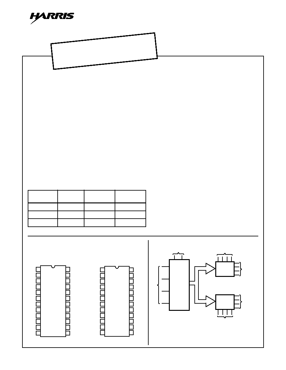
CD22101 and CD22102 crosspoint switches consist of
4 x 4 x 2 arrays of crosspoints (transmission gates) with a
4-line to 16-line decoder and 16 latch circuits. Any one of
the sixteen crosspoint pairs can be selected by applying
the
appropriate
four-line
address,
corresponding
crosspoints in each array are turned on and off
simultaneously. Any number of crosspoints can be turned
on simultaneously.
In the CD22101, the selected crosspoint pair can be
turned on or off by applying a logic ONE or ZERO,
respectively, to the data input, and applying a ONE to the
strobe input. When the device is "powered up", the states
of the 16 switches are indeterminate. Therefore, all
switches must be turned off by putting the strobe high,
data-in
low,
and
then
addressing
all
switches
in
succession.
The selected pair of crosspoints in the CD22102 is turned
on by applying a logic ONE to the K
A
(set) input while a
logic ZERO is on the K
B
input, and turned off by applying
a logic ONE to the K
B
(reset) input while a logic ZERO is
on the K
A
input. In this respect, the control latches of the
CD22102 are similar to SET/RESET flip-flops. They differ,
however, in that the simultaneous application of ONEs to
the K
A
and K
B
inputs turns off (resets) all crosspoints. All
crosspoints in both devices must be turned off as V
DD
is
applied.
Features
� Low ON Resistance . . . . . . . . . . . . 75
(Typ) at V
DD
= 12V
� "Built - In" Latched Inputs
� Large Analog Signal Capability . . . . . . . . . . . . . . .
�
V
DD
/2
� Switch Bandwidth . . . . . . . . . . . . . . . . . . . . . . . . . . 10MHz
� Matched Switch Characteristics
R
ON
= 8
(Typ) at V
DD
= 12V
� High Linearity - 0.25% Distortion (Typ) at f = 1kHz,
V
IN
= 5V
P-P
, V
DD
- V
SS
= 10V, and R
L
= 1k
� Standard CMOS Noise Immunity
Applications
� Telephone Systems
� PBX
� Studio Audio Switching
� Multisystem Bus Interconnect
Ordering Information
PART
NUMBER
TEMP.
RANGE (
o
C)
PACKAGE
PKG. NO.
CD22101E
-40 to 85
24 Ld PDIP
E24.6
CD22101F
-55 to 125
24 Ld CERDIP
F24.6
CD22102E
-40 to 85
24 Ld PDIP
E24.6
February 1999
Pinouts
CD22101
(PDIP, SBDIP)
TOP VIEW
CD22102
(PDIP)
TOP VIEW
1
2
3
4
5
6
7
8
9
10
11
12
D
16
17
18
19
20
21
22
23
24
15
14
13
A
VDD
VSS
DATA
STROBE
X1'
Y2'
B
C
X2'
Y1'
X4'
X3'
Y4'
Y3'
X2
Y1
Y2
X4
X3
Y4
Y3
X1
1
2
3
4
5
6
7
8
9
10
11
12
D
16
17
18
19
20
21
22
23
24
15
14
13
A
VDD
VSS
X1'
Y2'
B
C
X2'
Y1'
X4'
X3'
Y4'
Y3'
X2
Y1
Y2
X4
X3
Y4
Y3
X1
K
A
K
B
Functional Diagram
4 X 4
SWITCH
4 X 4
SWITCH
16
16
ADDRESS
CONTROL
OUT (IN)
IN (OUT)
OUT (IN)
IN (OUT)
DECODER
LATCH
16
CD22101, CD22102
CMOS 4 x 4 x 2 Crosspoint Switch
with Control Memory
CAUTION: These devices are sensitive to electrostatic discharge. Users should follow proper IC Handling Procedures.
Copyright
�
Harris Corporation 1999
File Number
2871.3
[ /Title
(CD22
101,
CD221
02)
/Sub-
ject
(CMO
S 4 x 4
x 2
Cross-
point
Switch
with
Con-
trol
Mem-
ory)
/
Author
()
/Key-
words
(Har-
ris
Semi-
con-
ductor,
Tele-
com,
SLICs,
SLACs
, Tele-
phone,
Tele-
phony,
WLL,
Wire-
less
OBSOLETE PR
ODUCT
NO RECOMMENDED REPLA
CEMENT
Call Central Applications 1-800-442-7747
or email: centapp@harris.com

4-194
CD22101, CD22102
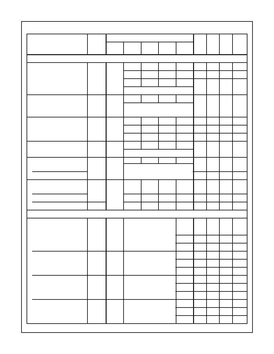
Absolute Maximum Ratings
Thermal Information
Supply Voltage (V
DD
) (Referenced to V
SS
Terminal) . . . .-0.5 to 20V
Input Voltage (All Inputs) . . . . . . . . . . . . . . . . . . . -0.5 to V
DD
+0.5V
Supply Voltage Range
For T
A
= Full Package Temperature Range . . . . . . . . . . . . . . 3V to 18V
Input Current (Any One Input) (Note 1)
. . . . . . . . . . . . . . . . . . .�
10mA
Power Dissipation
For T
A
= -40
o
C to 60
o
C (Package Type E) . . . . . . . . . . . . 500mW
For T
A
= 60
o
C to 85
o
C
Package Type E) . . . . . . . . Derate Linearly 12mW/
o
C to 200mW
For T
A
= -55
o
C to 100
o
C (Package Type D, F) . . . . . . . . . 500mW
For T
A
= 100
o
C to 125
o
C
(Package Type D, F) . . . . . Derate Linearly 12mW/
o
C to 200mW
Device Dissipation per Output Transistor
For T
A
= Full Package Temperature Range (All Types) . . . . . 100mW
Maximum Junction Temperature . . . . . . . . . . . . . . . . . . . . . . . 175
o
C
Maximum Junction Temperature (Plastic Package) . . . . . . . . 150
o
C
Maximum Storage Temperature Range . . . . . . -65
o
C
T
A
150
o
C
Maximum Lead Temperature (Soldering 10s) . . . . . . . . . . . . . 300
o
C
Operating Conditions
Temperature Range
Package Type D, F. . . . . . . . . . . . . . . . . . . . . -55
o
C
T
A
125
o
C
Package Type E . . . . . . . . . . . . . . . . . . . . . . . . -40
o
C
T
A
85
o
C
CAUTION: Stresses above those listed in "Absolute Maximum Ratings" may cause permanent damage to the device. This is a stress only rating and operation
of the device at these or any other conditions above those indicated in the operational sections of this specification is not implied.
Electrical Specifications
Values at -55
o
C, 25
o
C, 125
o
C Apply to D, F, H Packages
Values at -40
o
C, 25
o
C, 85
o
C Apply to E Package
PARAMETER
SYMBOL
TEST CONDITIONS
-55
o
C
-40
o
C
85
o
C
125
o
C
25
o
C
UNITS
FIGURE V
DD
(V)
MAX
MAX
MAX
MAX
MIN
TYP
MAX
STATIC CROSSPOINTS
Quiescent Device
Current
I
DD
(Max)
1
5
5
5
150
150
-
0.04
5
�
A
1
10
10
10
300
300
-
0.04
10
�
A
1
15
20
20
600
600
-
0.04
20
�
A
1
20
100
100
3000
3000
-
0.08
100
�
A
On Resistance
R
ON
(Max) Any Switch
V
IS
= 0 to
V
DD
14
5
475
500
725
800
-
225
600
15
10
135
145
205
230
-
85
180
-
12
100
110
155
175
-
75
135
16
15
70
75
110
125
-
65
95
ON
Resistance
R
ON
Between Any Two
Switches
5
-
-
-
-
-
25
-
10
-
-
-
-
-
10
-
12
-
-
-
-
-
8
-
15
-
-
-
-
-
5
-
OFF Leakage Current
I
L
(Max)
All Switches
OFF, V
IS
= 18V
4
18
�
1000
-
�
1
�
100
(Note 2)
nA
STATIC CONTROLS
Input Low Voltage
V
IL
(Max) OFF Switch I
L
< 0.2
�
A
5
1.5
-
-
1.5
V
10
3
-
-
3
V
15
4
-
-
4
V
Input High Voltage
V
IH
(Min)
ON Switch See R
ON
Characteristic
5
3.5
3.5
-
-
V
10
7
7
-
-
V
15
11
11
-
-
V
Input Current
I
IN
(Max)
Any Control
V
IN
= 0, 18V
2
18
�
0.1
�
0.1
�
1
�
1
-
�
10
-5
�
0.1
�
A
NOTES:
1. Maximum current through transmission gates (switches) = 25mA.
2. Determined by minimum feasible leakage measurement for automatic testing.
4-195
CD22101, CD22102
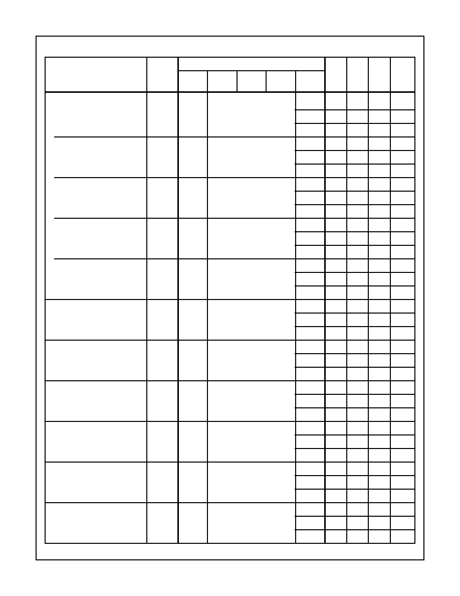
Electrical Specifications
T
A
= 25
o
C
PARAMETER
SYMBOL
TEST CONDITIONS
MIN
TYP
MAX
UNITS
FIGURE
f
IS
(kHz)
R
L
(k
)
V
IS
(V)
(Note 3)
V
DD
(V)
DYNAMIC CROSSPOINTS
Propagation Delay Time,
(Switch ON) Signal Input to Output
t
PHL
, t
PLH
5
-
-
5
5
-
30
60
ns
-
10
10
10
-
15
30
ns
15
15
-
10
20
ns
C
L
= 50pF; t
R
, t
F
= 20ns
Frequency Response (Any Switch
ON)
f
3dB
19
1
1
5
10
-
40
-
MHz
Sine Wave Input,
Sine Wave Response (Distortion)
THD
-
1
1
2.5
5
-
1
-
%
1
1
5
10
-
0.25
-
%
1
1
7.5
15
-
0.15
-
%
Feedthrough (All Switches OFF)
F
DT
13
1.6
0.6
2 (Note 4)
10
-
-96
-
dB
Sine Wave Input
Frequency for Signal Crosstalk
F
CT
12
-
0.6
1 (Note 4)
10
Attenuation of 40dB
Sine Wave Input
-
2.5
-
MHz
Attenuation of 95dB
0.1
kHz
Capacitance:
X
N
to Ground
C
IS
-
-
-
-
25
-
pF
Y
N
to Ground
-
-
-
-
60
-
pF
Feedthrough
C
IOS
-
-
-
-
0.6
-
pF
DYNAMIC CONTROLS
Propagation Delay Time: High
Impedance to High Level or Low
Level
t
PZH
, t
PZL
6
R
L
= 1k
, C
L
= 50pF,
t
R
, t
F
= 20ns
5
-
500
1000
ns
Strobe to Output, CD22101
10
-
230
460
ns
15
-
170
340
ns
Data-In to Output, CD22101
t
PZH
, t
PZL
7
R
L
= 1k
, C
L
= 50pF,
t
R
, t
F
= 20ns
5
-
515
1000
ns
10
-
220
440
ns
15
-
170
340
ns
K
A
to Output, CD22102
t
PZH
, t
PZL
-
R
L
= 1k
, C
L
= 50pF,
t
R
, t
F
= 20ns
5
-
500
1000
ns
10
-
215
430
ns
15
-
160
320
ns
Address to Output
CD22101, CD22102
t
PZH
, t
PZL
8
R
L
= 1k
, C
L
= 50pF,
t
R
, t
F
= 20ns
5
-
480
960
ns
10
-
225
450
ns
15
-
155
300
ns
20log
V
OS
V
IS
-----------
-3dB
=
4-196
CD22101, CD22102
Propagation Delay Time: High Level
or Low Level to High Impedance
t
PHZ,
t
PLZ
6
R
L
= 1k
, C
L
= 50pF,
t
R
, t
F
= 20ns
5
-
450
900
ns
Strobe to Output, CD22101
10
-
200
400
ns
15
-
135
270
ns
K
B
to Output, CD22102
t
PHZ,
t
PLZ
-
R
L
= 1k
, C
L
= 50pF,
t
R
, t
F
= 20ns
5
-
450
900
ns
10
-
200
400
ns
15
-
130
260
ns
Data-In to Output, CD22101
t
PHZ,
t
PLZ
-
R
L
= 1k
, C
L
= 50pF,
t
R
, t
F
= 20ns
5
-
450
900
ns
10
-
165
330
ns
15
-
110
220
ns
K
A
�
K
B
to Output, CD22102
t
PHZ,
t
PLZ
-
R
L
= 1k
, C
L
= 50pF,
t
R
, t
F
= 20ns
5
-
280
560
ns
10
-
130
260
ns
15
-
90
180
ns
Address to Output
CD22101, CD22102
t
PHZ,
t
PLZ
8
R
L
= 1k
, C
L
= 50pF,
t
R
, t
F
= 20ns
5
-
425
850
ns
10
-
190
380
ns
15
-
130
260
ns
Minimum Strobe Pulse Width,
CD22101
t
W
6
R
L
= 1k
, C
L
= 50pF,
t
R
, t
F
= 20ns
5
-
260
500
ns
10
-
120
240
ns
15
-
80
160
ns
Address to Strobe Setup or Hold
Times, CD22101
t
SU,
t
H
9
R
L
= 1k
, C
L
= 50pF,
t
R
, t
F
= 20ns
5
-
-160
0
ns
10
-
-70
0
ns
15
-
-50
0
ns
Strobe to Data-In Hold Time,
CD22101
t
HHL
, t
HLH
10
R
L
= 1k
, C
L
= 50pF,
t
R
, t
F
= 20ns
5
-
200
400
ns
10
-
80
160
ns
15
-
60
120
ns
Address to K
A
and K
B
Setup or Hold
Times, CD22102
t
SU
, t
H
-
R
L
= 1k
, C
L
= 50pF,
t
R
, t
F
= 20ns
5
-
-160
0
ns
10
-
-70
0
ns
15
-
-50
0
ns
Minimum K
A
�
K
B
Pulse Width,
CD22102
t
W
-
R
L
= 1k
, C
L
= 50pF,
t
R
, t
F
= 20ns
5
-
375
750
ns
10
-
160
320
ns
15
-
110
220
ns
Minimum K
A
Pulse Width, CD22102
t
W
-
R
L
= 1k
, C
L
= 50pF,
t
R
, t
F
= 20ns
5
-
425
850
ns
10
-
175
350
ns
15
-
120
240
ns
Electrical Specifications
T
A
= 25
o
C (Continued)
PARAMETER
SYMBOL
TEST CONDITIONS
MIN
TYP
MAX
UNITS
FIGURE
f
IS
(kHz)
R
L
(k
)
V
IS
(V)
(Note 3)
V
DD
(V)

4-197
CD22101, CD22102
Functional Block Diagram
Minimum K
B
Pulse Width, CD22102
t
W
-
R
L
= 1k
, C
L
= 50pF,
t
R
, t
F
= 20ns
5
-
200
400
ns
10
-
90
180
ns
15
-
70
140
ns
Control Crosstalk, Data-In, Address
or Strobe to Output
11
100
10
5
-
75
-
mV
PEAK
Square Wave Input = 5V,
t
R
, t
F
= 20ns, R
S
= 1k
Input Capacitance
C
IN
Any Control Input
-
-
5
7.5
pF
NOTES:
3. Peak-to-peak voltage symmetrical about
, unless otherwise specified.
4. RMS.
Electrical Specifications
T
A
= 25
o
C (Continued)
PARAMETER
SYMBOL
TEST CONDITIONS
MIN
TYP
MAX
UNITS
FIGURE
f
IS
(kHz)
R
L
(k
)
V
IS
(V)
(Note 3)
V
DD
(V)
V
DD
2
-----------
SIGNALS IN (OUT)
SIGNALS IN (OUT)
SIGNALS
OUT (IN)
SIGNALS
OUT (IN)
0
1
2
3
7
6
5
4
8
12
13
9
10
11
15
14
Y1
Y2
Y3
Y4
17
16
20
21
19
18
22
15
X1
X2
X3
X4
0'
1'
2'
3'
7'
6'
5'
4'
8'
12'
13'
9'
10'
11'
15'
14'
Y1'
Y2'
Y3'
Y4'
8
9
5
4
6
7
3
10
X1'
X2'
X3'
X4'
16
16
16
16
14
13
CD22102
ONLY
K
A
K
B
CD22101
ONLY
STROBE
DATA
ADDRESS
D
11
DECODER
2
1
23
C
B
A
LATCHES
(NOTE)
INPUTS PROTECTED
BY COS/MOS
PROTECTION
NETWORK
V
DD
V
SS
(NOTE)
(NOTE)
(NOTE)
(NOTE)
(NOTE)
NOTE: