 | –≠–ª–µ–∫—Ç—Ä–æ–Ω–Ω—ã–π –∫–æ–º–ø–æ–Ω–µ–Ω—Ç: CD22103AD | –°–∫–∞—á–∞—Ç—å:  PDF PDF  ZIP ZIP |
68
CAUTION: These devices are sensitive to electrostatic discharge; follow proper IC Handling Procedures.
http://www.intersil.com or 407-727-9207 | Copyright © Intersil Corporation 1999
CD22103A
CMOS HDB3 (High Density Bipolar 3)
Transcoder for 2.048/8.448Mb/s
Transmission Applications
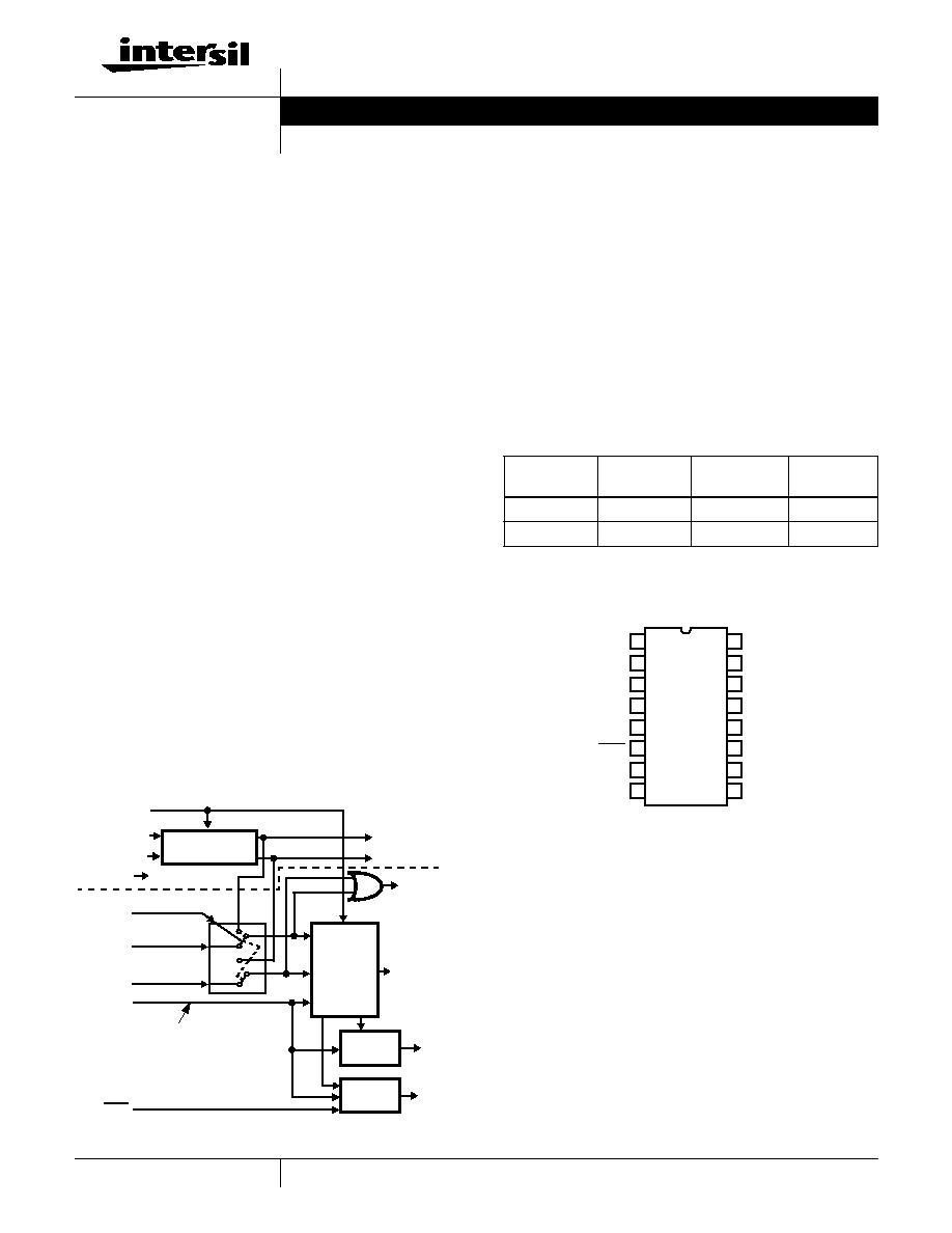
The CD22103A is an LSI SOS integrated circuit which
performs the HDB3 transmission coding and reception
decoding functions with error detection. It is used in
2.048Mb/s and 8.448Mb/s transmission applications. The
CD22103A performs HDB3 coding and decoding for data
rates from 50Kb/s to 10Mb/s in a manner consistent with
CCITT G703 recommendations.
HDB3 transmission coding/reception decoding with code
error detection is performed in independent coder and
decoder sections. All transmitter and receiver inputs/outputs
are TTL compatible.
The HDB3 transmitter coder codes an NRZ binary unipolar
input signal (NRZ-IN) and a synchronous transmission clock
(CTX) into two HDB3 binary unipolar RZ output signals
(+HDB3 OUT, -HDB3 OUT). The TTL compatible output
signals +HDB3 OUT, -HDB3 OUT are externally mixed to
generate ternary bipolar HDB3 signals for driving
transmission lines.
The receiver decoder converts binary unipolar inputs
(+HDB3 IN, -HDB3 IN), which were externally split from
ternary bipolar HDB3 signals, and a synchronous clock
signal (CRX) into binary unipolar NRZ signals (NRZ-OUT).
The CD22103A operates with a 5V
±
10% power supply
voltage over the full military temperature range at data rates
from 50Kb/s up to 10Mb/s.
Block Diagram
Features
∑ HDB3 Coding and Decoding for Data Rates from 50Kb/s
to 10Mb/s in a Manner Consistent with CCITT G703
Recommendations
∑ HDB3/AMI Transmission Coding/Reception Decoding with
Code Error Detection is Performed in Independent Coder
and Decoder Sections
∑ All Transmitter and Receiver Inputs/Outputs are TTL
Compatible
∑ Internal Loop Test Capability
∑ Pin and Functionally Compatible with Type MJ1471
Pinout
CD22103A (PDIP, SBDIP)
TOP VIEW
TRANSMITTER
CODER
RECEIVER
DECODER
AIS
DETECT
ERROR
DETECT
NRZ-IN
CTX
HDB3/AMI
NRZ-OUT
CRX
AIS
RAIS
LTE
CKR
ERR
+HDB3 OUT
-HDB3 OUT
+HDB3 IN
-HDB3 IN
ENCODER
IN
DECODER
REQUIRES CLOCK
RECOVERY CIRCUIT
Ordering Information
PART
NUMBER
TEMP. RANGE
(
o
C)
PACKAGE
PKG. NO.
CD22103AD
-55 to 125
16 Ld SBDIP
D16.3
CD22103AE
-40 to 85
16 Ld PDIP
E16.3
14
15
16
9
13
12
11
10
1
2
3
4
5
7
6
8
NRZ-IN
CTX
HDB3/AMI
NRZ-OUT
CRX
AIS
LTE
CKR
ERR
V
DD
V
SS
+HDB3 OUT
-HDB3 OUT
+HDB3 IN
-HDB3 IN
RAIS
Data Sheet
January 1997
File Number
1310.3
69
Absolute Maximum Ratings
Thermal Information
Supply Voltage (V
DD
)
(Voltages referenced to V
SS
Terminal) . . . . . . . . . . . . . -0.5 to 8V
Supply Voltage Range
For T
A
= Full Package Temperature Range . . . . . . . . . . . . 4.5V to 5.5V
Input Voltage (All Inputs) . . . . . . . . . . . . . . . . . . . -0.5 to V
DD
+0.5V
Input Current (Any One Input)
. . . . . . . . . . . . . . . . . . . . . . . . . . .±
10mA
Power Dissipation
For T
A
= -40
o
C to 60
o
C (Package Type E) . . . . . . . . . . . . .500mW
For T
A
= 60
o
C to 85
o
C
(Package Type E) . . . . . . . . Derate Linearly 12mW/
o
C to 200mW
For T
A
= -55
o
C to 100
o
C (Package Type D). . . . . . . . . . . .500mW
For T
A
= 100
o
C to 125
o
C
(Package Type D) . . . . . . . . Derate Linearly 12mW/
o
C to 200mW
Device Dissipation per Output Transistor
For T
A
= Full Package Temperature Range (All Types) . . . . . 100mW
Maximum Junction Temperature . . . . . . . . . . . . . . . . . . . . . . .175
o
C
Maximum Junction Temperature (Plastic Package) . . . . . . . . .150
o
C
Maximum Storage Temperature Range . . . . . . . -65
o
C
T
A
150
o
C
Maximum Lead Temperature (Soldering 10s) . . . . . . . . . . . . .300
o
C
Operating Conditions
Temperature Range
Package Type D . . . . . . . . . . . . . . . . . . . . . . . -55
o
C
T
A
125
o
C
Package Type E . . . . . . . . . . . . . . . . . . . . . . . . -40
o
C
T
A
85
o
C
CAUTION: Stresses above those listed in "Absolute Maximum Ratings" may cause permanent damage to the device. This is a stress only rating and operation of the
device at these or any other conditions above those indicated in the operational sections of this specification is not implied.
Electrical Specifications
V
DD
= 5V
±
10%, T
A
= 25
o
C
PARAMETER
SYMBOL
TEST CONDITIONS
MIN
TYP
MAX
UNITS
STATIC SPECIFICATIONS
Quiescent Device Current
I
DD
-
-
100
µ
A
Operating Device Current
f
CL
= 10MHz
-
-
8
mA
HDB3 Output Low (Sink) Current
I
OL1
V
OL
= 0.5V
1.6
-
-
mA
HDB3 Output High (Source) Current
I
OH1
V
OH
= 2.8V
-10
-
-
mA
All Other Outputs Low (Sink) Current
I
OL2
V
OL
= 0.5V
1.6
-
-
mA
All Other Outputs High (Source) Current
I
OH2
V
OH
= 2.8V
-1.6
-
-
mA
Input Low Current
I
IL
-
-
-1
µ
A
Input High Current
I
IH
-
-
1
µ
A
Input Low Voltage
V
IL
-
-
0.8
V
Input High Voltage
V
IH
2
-
-
V
Input Capacitance
I
IN
-
-
5
pF
Electrical Specifications
T
A
= -40
o
C to 85
o
C for Plastic Package; -55
o
C to 125
o
C for Ceramic Package; V
DD
= 4.5V to 5.5V;
C
L
= 15pF
PARAMETER
SYMBOL
FIGURE
MIN
TYP
MAX
UNITS
DYNAMIC INPUT
CTX, CRX Input Frequency
f
CTX
, f
CRX
0.05
-
10
MHz
CTX, CRX Input Rise Time
t
RCL
3
-
-
1
µ
s
Fall Time
t
FCL
3
-
-
1
µ
s
NRZ-IN to CTX
Data Setup Time
t
S
3
15
-
-
ns
Data Hold Time
t
H
3
15
-
-
ns
HDB3 IN to CRX
Data Setup Time
t
S
4
15
-
-
ns
Data Hold Time
t
H
3
0
-
-
ns
CD22103A
70
Functional Description
The CD22103A is designed to code and decode HDB3
signals which are coded as binary digital signals (NRZ-lN)
and (+HDB3 IN, -HDB3 IN), accompanied by sampling
clocks (CTX) and (CRX). The two binary coded HDB3 out-
puts, (+HDB3 OUT, -HDB3 OUT) may be externally mixed to
create the ternary HDB3 signals (See Figure 1).
The two binary HDB3 input signals have been split from the
input ternary HDB3 in an external line receiver.
The receiver decoder converts binary unipolar inputs (+HDB3 IN,
-HDB3 IN), which were externally split from ternary bipolar HDB3
signals, and a synchronous clock signal (CRX) into binary unipolar
NRZ signals (NRZ-OUT).
Received signals not consistent with HDB3 coding rules are
detected as errors. The receiver error output (ERR) is active high
during one CRX period of each bit of received data that is inconsis-
tent with HDB3 coding rules.
An input string consisting of all ones (or marks) is detected and
signaled by a high level at the Alarm Signal (AIS) output. The AIS
output is set to a high level when less than three zeros are
received during two consecutive periods of the Reset Alarm Inhibit
Signal (RAIS). The AIS output is subsequently reset to a low level
when three or more zeros are received during two periods of the
reset signal (RAIS).
A diagnostic Loop-Test Mode may be entered by driving the Loop
Test Enable Input (LTE) high. In this mode the HDB3 transmitter
outputs (+HDB3 OUT, -HDB3 OUT) are internally connected to
the HDB3 receiver inputs, and the external HDB3 receiver inputs,
and the external HDB3 receiver inputs (+HDB3 IN, -HDB3 IN) are
disabled. The NRZ binary output signal (NRZ - OUT) corresponds
to the NRZ binary input signal (NRZ - IN) delayed by approxi-
mately 8 clock periods.
The Clock Receiver Output (CKR) is the product of the two HDB3
input signals or-ed together. The CRX clock signal may be derived
from the CKR signal with external clock extraction circuitry. In the
Loop Test Mode (LTE = 1) CKR is the product of the +HDB3 OUT
and -HDB3 OUT signals or-ed together.
The CD22103A may also be used to perform the AMI to NRZ
coding/decoding function. To use the CD22103A in this mode, the
HDB3/AMI control input is driven low.
Error Detection
Received HDB3/AMl binary input signals are checked for
coding violations, and an error signal (ERR) is generated as
described below.
∑ HDB3 Signals HDB3/AMl = High
The error signal (ERR) is flagged high for one CTX period if
a violation pulse (
±
V) is received of the same polarity as the
last received violation pulse.
A violation pulse (
±
V) is considered a reception error and
does not cause replacement of the last string of 4 bits to
zeros, if:
CRX to CKR (CRX = 8.448MHz)
Pretrigger
t
P
5
-
-
20
ns
Delay
t
D
5
-
-
20
ns
DYNAMIC OUTPUT
Transmitter Coder, CTX to HDB3 OUT:
Data Propagation Delay Time
t
DD
3
-
-
90
ns
Handling Delay Time
t
HD
1
-
4
-
Clock Period
HDB3 OUT Output Pulse Width
(Clock duty cycle = 50%)
f
CL
= 2.048MHz
t
W
3
238
-
260
ns
f
CL
= 8.448MHz
t
W
3
53
-
65
Receiver Decoder
CRX to NRZ OUT:
Data Propagation Delay Times
t
DD
4
-
-
90
ns
Handling Delay Time
t
HD
2
-
4
-
Clock Period
HDB3 IN to CKR
HDB3 Propagation Delay Time
LTE = 0
t
IN CKR
4
-
-
65
ns
LTE = 1
4
-
-
30
ns
Electrical Specifications
T
A
= -40
o
C to 85
o
C for Plastic Package; -55
o
C to 125
o
C for Ceramic Package; V
DD
= 4.5V to 5.5V;
C
L
= 15pF (Continued)
PARAMETER
SYMBOL
FIGURE
MIN
TYP
MAX
UNITS
CD22103A
71
The received 4 data bits previous to reception of the violation
pulse have not been the sequence BX00 (where X = don't
care). The error signal (ERR) remains low.
NOTES:
1. The data sequences B000V and BB00V are valid HDB3 codings
of the NRZ binary sequence 10000.
2. The error signal (ERR) count, is the accurate number of all single
bit errors.
∑ AMl Signals HDB3/AMl = Low
- A coding error (ERR) is signaled when a violation pulse
(+V) is received.
∑ In Either the HDB3 or AMI Mode
- When high levels appear simultaneously on both HDB3
inputs (+ HDB3 IN, -HDB3 IN) a logical one is assumed
in the HDB3/AMl input stream and the error signal
(ERR) goes high for the duration of the violation.
Alarm Inhibit Signal
- The alarm output (AIS) is set high if, in two successive
periods of the external Reset Alarm Signal (RAlS), less
than three zeros are received.
- The alarm output (AlS) is reset low when three or more
zeros are received during two Reset Alarm Signal periods.
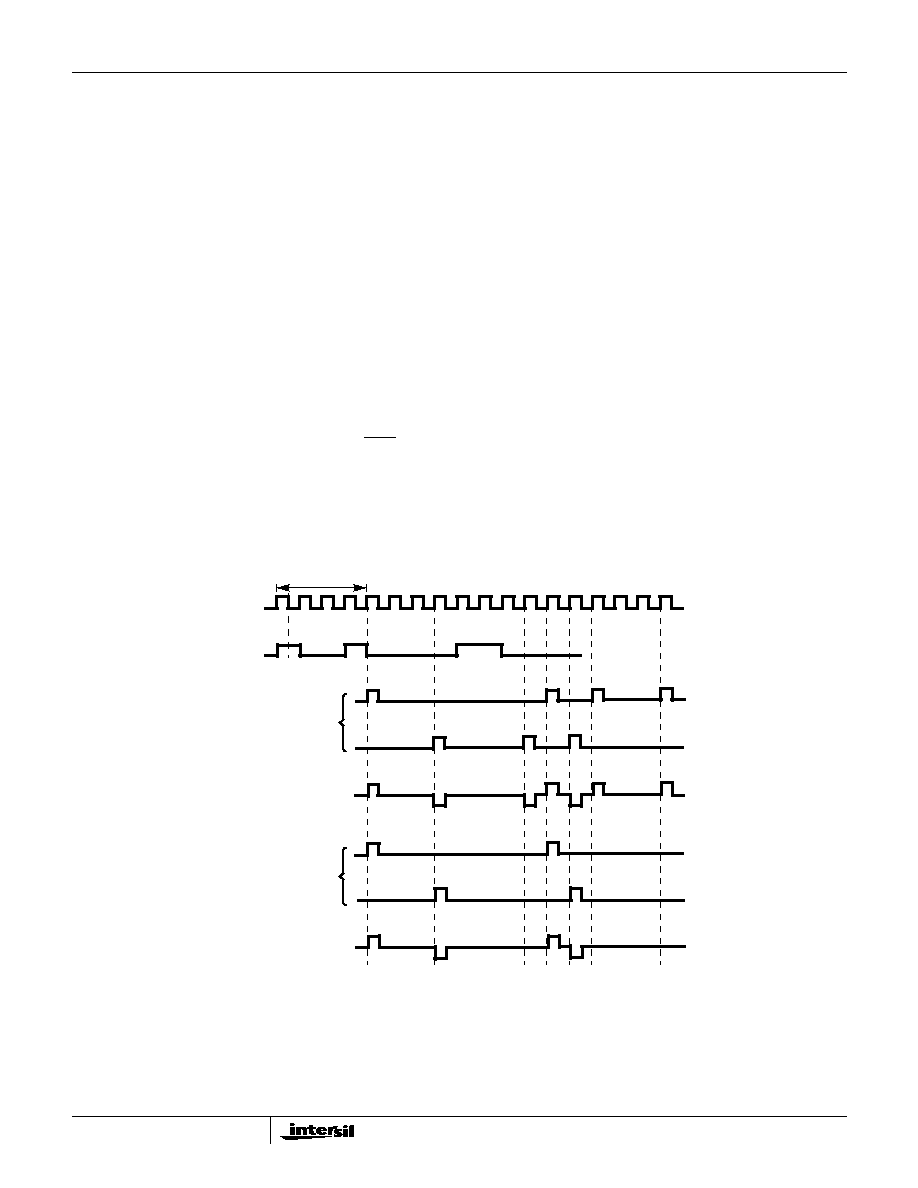
Transcoder Operation
Transmitter Coder (See Figure 1)
The HDB3/AMI transmitter coder operates on 4-bit serial
strings of NRZ binary data and a synchronous transmitter
clock (CTX). NRZ binary data is serially clocked into the
transmitter on the negative transition of the (CTX) clock.
HDB3/AMI coding is performed on the 4-bit string, and
HDB3/AMI binary output data is clocked out to the (+HDB3
OUT, -HDB3 OUT) outputs on the positive transition of the
transmitter clock (CTX) 3 1/2 clock pulses after the data
appeared at the (NRZ-IN) input.
Receiver Decoder (See Figure 2)
The HDB3/AMI receiver decoder operates on 4-bit serial
strings of binary coded HDB3/AMI signals, and a synchro-
nous receiver clock (CRX), HDB3/AMI binary data is serially
clocked into the receiver on the positive transition of the
(CRX) clock. HDB3/AMI decoding is performed on the 4-bit
string, and NRZ binary output data is clocked out to the
(NRZ-OUT) output on the positive transition of the receiver
clock (CRX) 4 clock pulses after the data appeared at the
(+HDB3 IN, -HDB3 IN) inputs.
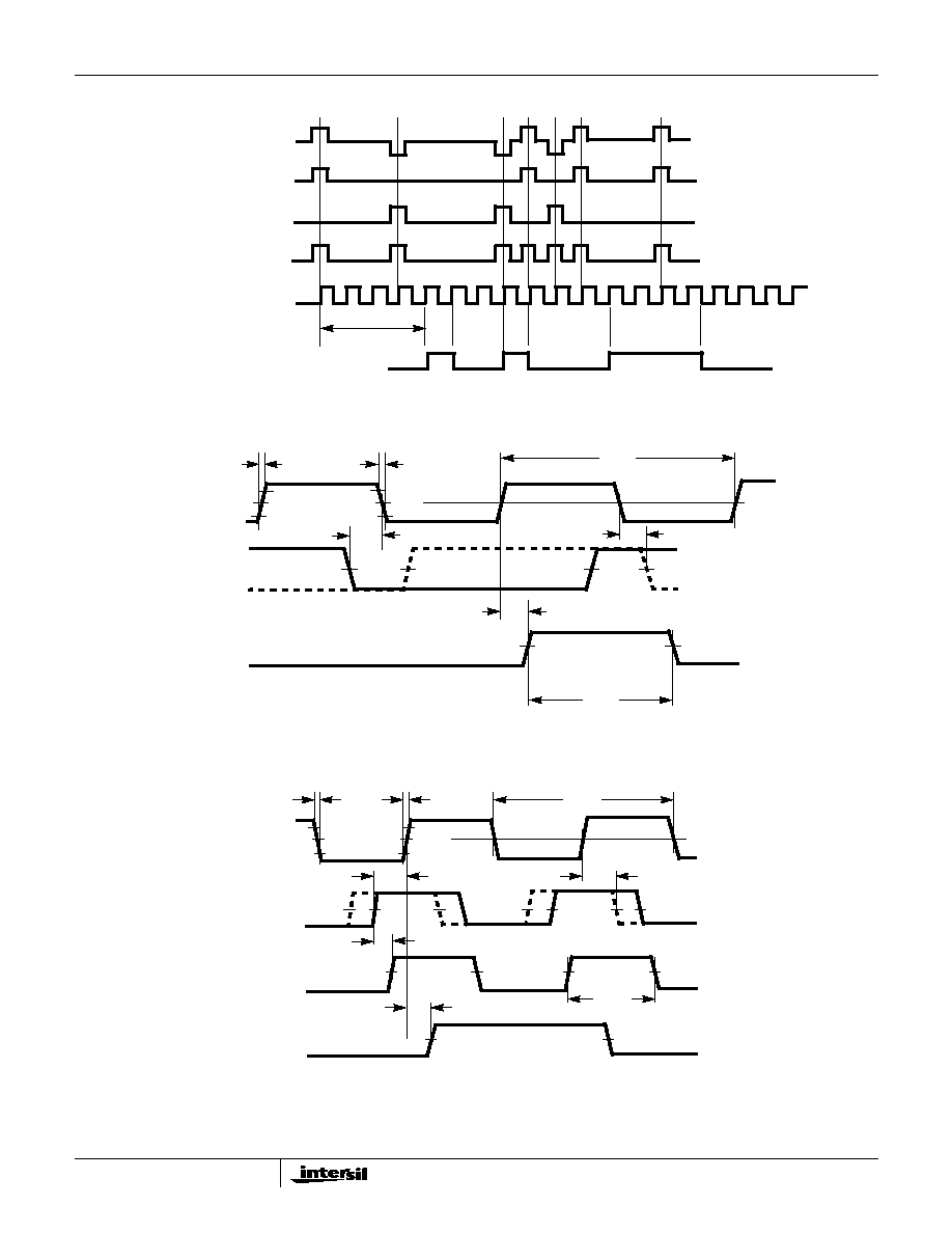
HANDLING DELAY
NRZ - IN
+HDB3 OUT
HDB3
CODED
-HDB3 OUT
EXTERNAL GENERATED
TERNERY HDB3
+HDB3 OUT
AMI
CODED
-HDB3 OUT
EXTERNAL GENERATED
AMI
CTX
FIGURE 1. TRANSMITTER CODER OPERATION TIMING WAVEFORMS - NRZ TO HDB3/AMI CODING
CD22103A
72
FIGURE 2. RECEIVER DECODER OPERATION TIMING WAVEFORMS - HDB3 TO NRZ DECODING
FIGURE 3. TRANSMITTER CODER TIMING WAVEFORMS
FIGURE 4. INPUT REQUIREMENTS AND OUTPUT CHARACTERISTICS
CKR
-HDB3 IN
+HDB3 IN
HDB3 RECEIVED SIGNAL
EXTERNALLY
SPLIT
CRX
EXTERNALLY
GENERATED
NRZ - OUT
HANDLING DELAY
t
RCL
t
FCL
t
W
CL
t
S
t
H
t
DD
t
W
NRZ - IN
+HDB3 OUT
OR
-HDB3 OUT
10%
90%
50%
CTX
90%
50%
10%
50%
50%
t
FCL
t
RCL
t
W
CL
t
S
t
H
t
DD
t
W
50%
50%
50%
+HDB3 IN
-HDB3 IN
CKR
NRZ - OUT
t
INCKR
CRX
CD22103A