 | –≠–ª–µ–∫—Ç—Ä–æ–Ω–Ω—ã–π –∫–æ–º–ø–æ–Ω–µ–Ω—Ç: CD22402D | –°–∫–∞—á–∞—Ç—å:  PDF PDF  ZIP ZIP |
8-40
Semiconductor
May 1999
CD22402
Sync Generator for TV Applications
and Video Processing Systems
Features
∑ Interlaced Composite Sync Output
∑ Automatic Genlock Capability
∑ Crystal Oscillator Operation
∑ 525 or 625 Line Operation
∑ Vertical Reset Option
∑ Wide Power Supply Operating Voltage . . . . . 4V to 15V
Applications
∑ Cameras
∑ Monitors and Displays
∑ CATV
∑ Teletext
∑ Video Games
∑ Sync Restorer
∑ Video Service Instruments
Description
The Harris CD22402 (Note) is a CMOS LSI sync generator that
produces all the timing signals required to drive a fully 2-to-1
interlaced 525-line 30-frame/second, or 625-line 25-frame/sec-
ond TV camera or video processing system. A complete sync
waveform is produced which begins each field with six serrated
vertical sync pulses, preceded and followed by six half-width
double frequency equalizing pulses. The sync output is gated by
the master clock to preserve horizontal phase continuity during
the vertical interval.
The CD22402 can be operated either in "genlock" mode, in
which it is synchronized with a reference sync pulse train from
another TV camera, or in "stand-alone" mode, in which it is syn-
chronized with a local on-chip crystal oscillator (the crystal and
two passive components are off chip). Also, the circuit can
sense the presence or absence of a reference sync pulse train
and automatically select the "genlock" or "stand-alone" mode.
A frame sync pulse is produced at the beginning of every odd
field. The vertical counter can be reset to either the first equalizing
pulse or the first vertical sync pulse of the vertical interval. The
interlaced sync provided by the CD22402 differs from RS-170 by
having slightly narrower sync and equalizing pulses. The clock
frequency of 32 times horizontal rate allows for approximately 4
µ
s
horizontal pulse widths and 2
µ
s equalizing pulses. Otherwise
operation can be phase locked to a color sub-carrier for a full
interlaced operating system.
The CD22402 is operable with a single supply over a voltage
range of 4V to 15V.
Pinout
CD22402 (PDIP, SBDIP)
TOP VIEW
Part Number Information
PART NUMBER
TEMP.
RANGE (
o
C)
PACKAGE
PKG.
NO.
CD22402D
-55 to 125
24 Ld SBDIP
D24.6
CD22402E
-40 to 85
24 Ld PDIP
E24.6
1
2
3
4
5
6
7
8
9
10
11
12
MIXED SYNC OUTPUT
VERTICAL DRIVE OUTPUT
HORIZONTAL CLAMP OUTPUT
16
17
18
19
20
21
22
23
24
15
14
13
FRAME SYNC OUTPUT (ODD FIELD)
HORIZONTAL PROCESSING BLANKING OUTPUT
MIXED PROCESSING BLANKING OUTPUT
MASTER FREQUENCY INPUT
DELAY, GENLOCK TO CRYSTAL OSCILLATOR
CRYSTAL OSCILLATOR FEEDBACK TAP
HORIZONTAL DRIVE OUTPUT
MIXED BEAM BLANKING OUTPUT
GENLOCK OSCILLATOR CAPACITOR CONNECTION
VERTICAL COUNTER RESET TO FIRST EQUALIZING PULSE
VERTICAL RESET TO FIRST VERTICAL SYNC PULSE
SHORT VERTICAL DRIVE OUTPUT
525 LINE TO 625 LINE OPERATION SWITCH
VERTICAL PROCESSING BLANKING OUTPUT
R-C CONNECTION FOR GENLOCK OSCILLATOR
DELAY, GENLOCK TO CRYSTAL OSCILLATOR
GENLOCK INPUT (COMPOSITE SYNC)
RESISTOR CONNECTION FOR GENLOCK OSCILLATOR
V
SS
V
SS
V
DD
CAUTION: These devices are sensitive to electrostatic discharge. Users should follow proper IC Handling Procedures.
Copyright
©
Harris Corporation 1999
File Number
1686.5
[ /Title
(CD2240
2)
/Subject
(Sync
Genera-
tor for
TV
Applica-
tions and
Video
Process-
OBSOLETE PR
ODUCT
NO RECOMMENDED REPLA
CEMENT
Call Central Applications 1-800-442-7747
or email: centapp@harris.com
8-41
Pin Descriptions
PIN NO.
SYMBOL
DESCRIPTION
1
XRC
Delay, Genlock to Crystal Oscillator. Resistor, diode and capacitor connection for delay that automatically
turns on the crystal oscillator when the genlock input is removed. When the signal on Terminal 1 is high the crys-
tal oscillator is inhibited. Typical values for R and C are 1M
and 0.001
µ
F. For operation as a crystal controlled
stand alone sync generator without genlock, Terminal 1 should be hardwired to V
SS
.
2
XTP
Crystal Oscillator Feedback Tap. Feedback connection (tap) for crystal oscillator. When a crystal (shunted by
a 1M
resistor) is connected between this terminal and Terminal 23, and a 100pF capacitor is connected from
this terminal to V
SS
, the sync generator creates its own master frequency. For a 525-line, 30-frame/second ras-
ter, the crystal frequency is 504.000kHz (Note 1); and for a 625-line, 25-frame/second raster, the crystal frequen-
cy is 500.000kHz (Note 1).
3
V
SS
Negative Power Supply Voltage. This terminal must be hardwired to Terminal 12 (V
SS
).
4
HD
Horizontal Drive Output
5
MS
Mixed Sync Output
6
C
Capacitor Connection for R-C Genlock Oscillator
7
MBB
Mixed Beam Blanking Output
8
VRE
Vertical Counter Reset to First Equalizing Pulse. A low level signal on this terminal resets the vertical counter
to the first equalizing pulse of a field. When not in use this terminal should be connected to V
DD
.
9
VD
Vertical Drive Output
10
VRV
Vertical Counter Reset to First Vertical Sync Pulse. A low level signal on this terminal resets the sync gen-
erator to the first vertical sync pulse of a field. For genlock operation, Terminal 10 is used as a resistor and ca-
pacitor connection for an integrator network that detects vertical sync pulses in a master sync waveform to which
the sync generator is to be genlocked. R is 22k
, and C is 0.001
µ
F. When not in use this terminal should be
connected to V
DD
.
11
HC
Horizontal Clamp Output
12
V
SS
Negative Power Supply Voltage
13
MPB
Mixed Processing Blanking Output
14
HPB
Horizontal Processing Blanking Output
15
FS2
Frame Sync Output (Odd Field). A pulse coinciding with the first equalizing pulse is produced at the beginning
of every odd field.
16
SVD
Short Vertical Drive Output
17
VPB
Vertical Processing Blanking Output
18
SW
Operation Switch for 525-Line or 625-Line Raster. A high level signal on Terminal 18 causes the sync gener-
ator to generate a 625-line raster. An internal pulldown resistor is connected to Terminal 18, so in the absence
of an applied input to this terminal, a 525-line raster is produced.
19
V
DD
Positive Power Supply Voltage. V
DD
can be any voltage between +4 and +15 relative to V
SS
.
20
GEN
Genlock Input Composite Sync. A negative going reference mixed sync waveform applied to Terminal 20 dis-
ables the crystal oscillator and locks the R-C genlock oscillator to the horizontal pulses of the reference sync
waveform. Vertical sync detection is achieved by an R-C integrator connected from Terminal 20 to Terminal 10
(vertical reset to first vertical sync pulse). An internal pull-up resistor is connected to Terminal 20 so that in the
absence of an applied input the crystal oscillator is enabled and the R-C genlock oscillator is disabled.
21
XR
Delay, Genlock to Crystal Oscillator, Resistor and Diode Connection for Delay, Genlock to Crystal Oscil-
lator. Automatically turns on the crystal oscillator when the input to Terminal 20 is removed.
22
RC
Resistor and Capacitor Connection for Genlock Oscillator. If the genlock oscillator is not used this terminal
should be connected to V
SS
. C should be 100pF, and R should be a 10k
potentiometer.
23
XIN
Master Frequency Input.
24
R
Resistor Connection for Genlock Oscillator.
NOTE: 32 times horizontal frequency.
CD22402
8-42
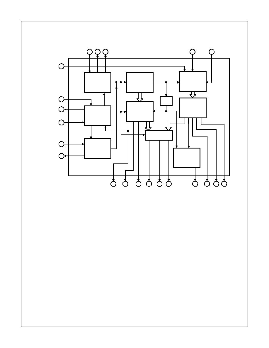
Block Diagram
CD22402 MONOCHROME TV SYNC GENERATOR WITH AUTOMATIC GENLOCK
R-C
GENLOCK
OSCILLATOR
˜
2
COMPOSITE
DECODER
AUTOMATIC
GENLOCK
CONTROL
CRYSTAL
OSCILLATOR
FRAME
SYNC
DECODER
FIELD
DECODER
HORIZONTAL
COUNTER
˜
16
VERTICAL
COUNTER
˜
525/625
LINE
DECODER
14
11
4
5
13
7
15
16
9
17
2
23
1
21
20
10
24
22
6
8
18
HPB
HC
HD
MS
MPB MBB
FS2
SVD
VD VPB
XTP
XIN
XRC
XR
GEN
R
VRV
RC
C
VRE
SW
V
SS
= PINS 3 AND 12
V
DD
= PIN 19
CD22402

8-43
Absolute Maximum Ratings
Thermal Information
DC Supply Voltage (Referenced to V
SS
Terminal) . . . . . . . . . . . 15V
Input Voltage Range, All Inputs (Notes 2, 3) . . . . . . V
SS
V
I
V
DD
DC Input Current, Any One Input (Note 2) . . . . . . . . . . . . . .
±
10mA
Operating Conditions
Temperature Range
CD22402D . . . . . . . . . . . . . . . . . . . . . . . . . . . . . -55
o
C to 125
o
C
CD22402E . . . . . . . . . . . . . . . . . . . . . . . . . . . . . . -40
o
C to 85
o
C
Thermal Resistance (Typical, Note 1)
JA
(
o
C/W)
JC
(
o
C/W)
SBDIP Package . . . . . . . . . . . . . . . . . .
50
10
PDIP Package . . . . . . . . . . . . . . . . . . .
50
N/A
Maximum Junction Temperature (SBDIP Package) . . . . . . . . 175
o
C
Maximum Junction Temperature (PDIP Package) . . . . . . . . 150
o
C
Maximum Storage Temperature Range . . . . . . . . . -65
o
C to 150
o
C
Maximum Lead Temperature (Soldering 10s) . . . . . . . . . . . . 300
o
C
(SOIC - Lead Tips Only)
CAUTION: Stresses above those listed in "Absolute Maximum Ratings" may cause permanent damage to the device. This is a stress only rating and operation
of the device at these or any other conditions above those indicated in the operational sections of this specification is not implied.
NOTES:
1.
JA
is measured with the component mounted on an evaluation PC board in free air.
2. To prevent damage to the input protection circuit, input signals should never be greater than V
DD
nor less than V
SS
. Input currents must
not exceed 10mA even when the power is off.
3. A connection must be provided at every input terminal. All unused inputs must be connected to V
DD
or V
SS
, whichever is appropriate.
Electrical Specifications
Values at -55
o
C, 25
o
C, 125
o
C Apply to D Package
Values at -40
o
C, 25
o
C, 85
o
C Apply to E Package
PARAMETER
SYMBOL
TEST
CONDITIONS
-55
o
C
-40
o
C
85
o
C
125
o
C
25
o
C
UNITS
V
O
(V)
V
DD
(V)
MIN
TYP
MAX
DC ELECTRICAL SPECIFICATIONS
Quiescent Device Current
I
DD
(Max)
-
5
-
-
-
-
0.5
0.75
1
mA
-
10
-
-
-
-
1.5
2
2.5
mA
-
15
-
-
-
-
3
4
5
mA
Output Low (Sink) Current
I
OL
(Min)
0.5
5
100
96
66
56
80
160
-
µ
A
5
5
1200
1155
787
672
960
1920
-
µ
A
0.5
10
248
239
164
140
200
400
-
µ
A
10
10
3000
2868
1968
1680
2400
4800
-
µ
A
Output High (Source) Cur-
rent
I
OH
(Min)
4.5
5
-100
-96
-66
-56
-80
-160
-
µ
A
0
5
-1200
-1155
-787
-672
-960
-1920
-
µ
A
9.5
10
-248
-239
-164
-140
-200
-400
-
µ
A
0
10
-3000
-2868
-1968
-1680
-2400
-4800
-
µ
A
Output Voltage Low Level
V
OL
(Max)
-
5
0.15
0.15
0.15
0.15
-
-
0.15
V
-
10
0.15
0.15
0.15
0.15
-
-
0.15
V
Output Voltage High Level
V
OH
(Min)
-
5
4.85
4.85
4.85
4.85
4.85
-
-
V
-
10
9.85
9.85
9.85
9.85
9.85
-
-
V
Input Low Voltage
V
IL
(Max)
0.5, 4.5
5
1.5
1.5
1.4
1.4
-
2.25
1.5
V
1, 9
10
3
3
2.9
2.9
-
4.5
3
V
Input High Voltage
V
IH
(Min)
0.5, 4.5
5
3.6
3.6
3.5
3.5
3.5
2.25
-
V
1, 9
10
7.1
7.1
7
7
7
4.5
-
V
Input Current
I
IN
(Max)
-
-
-
-
-
-
-
10
-
pA
Refer to the CD4000B Series data book 250.5 for general operating and application considerations.
CD22402
8-44
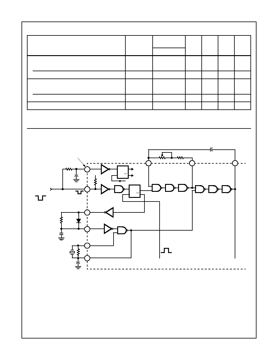
Logic Diagram
Switching Electrical Specifications
T
A
= 25
o
C and C
L
= 15pF. Typical Temperature Coefficient for All Values of V
DD
= 0.3%/
o
C
PARAMETER (NOTE 4)
SYMBOL
TEST
CONDITIONS
MIN
TYP
MAX
UNITS
V
DD
(V)
Output State Propagation Delay Time (50% to 50%)
Low-to-High Level
t
PLH
5
-
40
80
ns
High-to-Low Level
t
PHL
10
-
20
40
ns
Output State Transition Time (10% to 90%)
Low-to-High
t
TLH
5
-
45
90
ns
High-to-Low
t
THL
10
-
30
60
ns
Input Capacitance (Per Input)
C
I
-
-
5
-
pF
NOTE:
4. The characteristics given are defined for unbuffered gate in the CMOS process of the CD22402.
R
S
Q
Q
10
20
21
1
23
2
22
24
S
R
Q
Q
6
10K
10K
51pF
GENLOCK OSC.
+
1M
1N914
HOR.
DR
0.001
µ
F
100pF
1M
CRYSTAL
32 TIMES
HORIZ.
503.496kHz
(NOTE 5)
(NOTE 6)
HOR. PROCESS
BLANKING
CLOCK TO
COUNTERS
VERTICAL DRIVE (VERT. RESET
TO FIRST VERT. PULSE)
INTEGRATOR
GENLOCK
SYNC
NOTES:
5. Pin 21 high when pin 20 is high (or open).
6. Pin 1 high inhibits clock.
FIGURE 1. DETAIL OF THE OSCILLATOR/GENLOCK PORTION OF THE CD22402
CD22402