4-1
CD40160BMS, CD40161BMS, CD40162BMS,
CD40163BMS
CMOS Synchronous Programmable 4-Bit
Counters
CD40160BMS,
CD40161BMS,
CD40162BMS
and
CD40163BMS
are
4-bit
synchronous
programmable
counters. The CLEAR function of the CD40162BMS and
CD40163BMS is synchronous and a low level at the CLEAR
input sets all four outputs low on the next positive CLOCK
edge. The CLEAR function of the CD40160BMS and
CD40161BMS is asychronous and a low level at the CLEAR
input sets all four outputs low regardless of the state of the
CLOCK, LOAD, or ENABLE inputs. A low level at the LOAD
input disables the counter and causes the output to agree
with the setup data after the next CLOCK pulse regardless of
the conditions of the ENABLE inputs.
The carry look-ahead circuitry provides for cascading counters
for n-bit synchronous applications without additional gating.
Instrumental in accomplishing this function are two count-enable
inputs and a carry output (COUT). Counting is enabled when
both PE and TE inputs are high. The TE input is fed forward to
enable COUT. This enabled output produces a positive output
pulses with a duration approximately equal to the positive portion
of the Q1 output. This positive overflow carry pulse can be used
to enable successive cascaded stages. Logic transitions at the
PE or TE inputs may occur when the clock is either high or low.
The CD40160BMS through CD40163BMS types are functionally
equivalent to and pin-compatible with the TTL counter series
74LS160 through 74LS163 respectively.
The
CD40160BMS,
CD40161BMS,
CD40162BMS
and
CD40163BMS are supplied in these 16 lead outline packages:
Features
� High-Voltage Types (20V Rating)
� CD40160BMS Decade with Asynchronous Clear
� CD40161BMS Binary with Asynchronous Clear
� CD40162BMS Decade with Synchronous Clear
� CD40163BMS Binary with Synchronous Clear
� Internal Look-Ahead for Fast Counting
� Carry Output for Cascading
� Synchronously Programmable
� Clear Asynchronous Input (CD40160BMS, CD40161BMS)
� Clear Synchronous Input (CD40162BMS, CD40163BMS)
� Synchronous Load Control Input
� Low Power TTL Compatibility
� Standardized Symmetrical Output Characteristics
� 100% Tested for Quiescent Current at 20V
� Maximum Input Current of 1
�
A at 18V Over Full Package
Temperature Range; 100nA at 18V and +25
o
C
� Noise Margin (Over Full Package Temperature Range):
- 1V at VDD = 5V
- 2V at VDD = 10V
- 2.5V at VDD = 15V
� 5V, 10V and 15V Parametric Ratings
� Meets All Requirements of JEDEC Tentative Standard No. 13B,
"Standard Specifications for Description of `B' Series CMOS
Devices"
Applications
� Programmable Binary and Decade Counting
� Counter Control/Timers
� Frequency Dividing
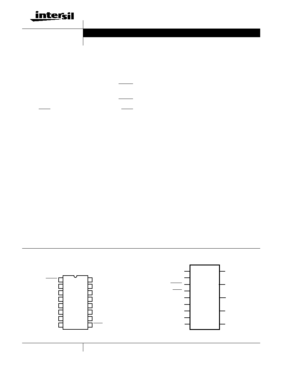
Pinout
CD40160BMS, CD40161BMS, CD40162BMS, CD40163BMS
TOP VIEW
Functional Diagram
CD40160 CD40161 CD40162 CD40163
Braze Seal DIP
H4W
H4X
H4X
H4W
Frit Seal DIP
H1F
H1F
H1L
H1F
Ceramic Flatpack
H6P
H6W
H6P
H6W
14
15
16
9
13
12
11
10
1
2
3
4
5
7
6
8
CLEAR
CLOCK
P1
P2
P3
P4
VSS
PE
VDD
Q1
Q2
Q3
Q4
TE
LOAD
CARRY OUT
7
6
10
1
9
2
3
4
5
LOAD
CLOCK
P1
P2
P3
P4
VSS = 8
TE
CLEAR
PE
Q1
Q2
Q3
Q4
CARRY
OUT
14
13
12
11
15
VDD = 16
December 1992
File Number
3358
CAUTION: These devices are sensitive to electrostatic discharge; follow proper IC Handling Procedures.
1-888-INTERSIL or 321-724-7143 | Copyright � Intersil Corporation 1999
4-2
Absolute Maximum Ratings
Reliability Information
DC Supply Voltage Range, (VDD) . . . . . . . . . . . . . . . . -0.5V to +20V
(Voltage Referenced to VSS Terminals)
Input Voltage Range, All Inputs . . . . . . . . . . . . . -0.5V to VDD +0.5V
DC Input Current, Any One Input
. . . . . . . . . . . . . . . . . . . . . . . . .�
10mA
Operating Temperature Range . . . . . . . . . . . . . . . -55
o
C to +125
o
C
Package Types D, F, K, H
Storage Temperature Range (TSTG). . . . . . . . . . . -65
o
C to +150
o
C
Lead Temperature (During Soldering) . . . . . . . . . . . . . . . . . +265
o
C
At Distance 1/16
�
1/32 Inch (1.59mm
�
0.79mm) from case for
10s Maximum
Thermal Resistance. . . . . . . . . . . . . . . .
ja
jc
Ceramic DIP and FRIT Package . . . .
80
o
C/W
20
o
C/W
Flatpack Package . . . . . . . . . . . . . . . .
70
o
C/W
20
o
C/W
Maximum Package Power Dissipation (PD) at +125
o
C
For T
A
= -55
o
C to +100
o
C (Package Type D, F, K). . . . . . .500mW
For T
A
= +100
o
C to +125
o
C (Package Type D, F, K) . . . . . Derate
Linearity at 12mW/
o
C to 200mW
Device Dissipation per Output Transistor. . . . . . . . . . . . . . . .100mW
For T
A
= Full Package Temperature Range (All Package Types)
Junction Temperature . . . . . . . . . . . . . . . . . . . . . . . . . . . . . .+175
o
C
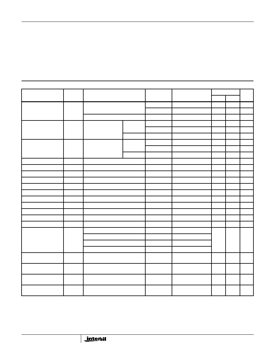
TABLE 1. DC ELECTRICAL PERFORMANCE CHARACTERISTICS
PARAMETER
SYMBOL
CONDITIONS (NOTE 1)
GROUP A
SUBGROUPS
TEMPERATURE
LIMITS
UNITS
MIN
MAX
Supply Current
IDD
VDD = 20V, VIN = VDD or GND
1
+25
o
C
-
10
�
A
2
+125
o
C
-
1000
�
A
VDD = 18V, VIN = VDD or GND
3
-55
o
C
-
10
�
A
Input Leakage Current
IIL
VIN = VDD or GND
VDD = 20
1
+25
o
C
-100
-
nA
2
+125
o
C
-1000
-
nA
VDD = 18V
3
-55
o
C
-100
-
nA
Input Leakage Current
IIH
VIN = VDD or GND
VDD = 20
1
+25
o
C
-
100
nA
2
+125
o
C
-
1000
nA
VDD = 18V
3
-55
o
C
-
100
nA
Output Voltage
VOL15
VDD = 15V, No Load
1, 2, 3
+25
o
C, +125
o
C, -55
o
C
-
50
mV
Output Voltage
VOH15
VDD = 15V, No Load (Note 3)
1, 2, 3
+25
o
C, +125
o
C, -55
o
C
14.95
-
V
Output Current (Sink)
IOL5
VDD = 5V, VOUT = 0.4V
1
+25
o
C
0.53
-
mA
Output Current (Sink)
IOL10
VDD = 10V, VOUT = 0.5V
1
+25
o
C
1.4
-
mA
Output Current (Sink)
IOL15
VDD = 15V, VOUT = 1.5V
1
+25
o
C
3.5
-
mA
Output Current (Source)
IOH5A
VDD = 5V, VOUT = 4.6V
1
+25
o
C
-
-0.53
mA
Output Current (Source)
IOH5B
VDD = 5V, VOUT = 2.5V
1
+25
o
C
-
-1.8
mA
Output Current (Source)
IOH10
VDD = 10V, VOUT = 9.5V
1
+25
o
C
-
-1.4
mA
Output Current (Source)
IOH15
VDD = 15V, VOUT = 13.5V
1
+25
o
C
-
-3.5
mA
N Threshold Voltage
VNTH
VDD = 10V, ISS = -10
�
A
1
+25
o
C
-2.8
-0.7
V
P Threshold Voltage
VPTH
VSS = 0V, IDD = 10
�
A
1
+25
o
C
0.7
2.8
V
Functional
F
VDD = 2.8V, VIN = VDD or GND
7
+25
o
C
VOH >
VDD/2
VOL <
VDD/2
V
VDD = 20V, VIN = VDD or GND
7
+25
o
C
VDD = 18V, VIN = VDD or GND
8A
+125
o
C
VDD = 3V, VIN = VDD or GND
8B
-55
o
C
Input Voltage Low
(Note 2)
VIL
VDD = 5V, VOH > 4.5V, VOL < 0.5V
1, 2, 3
+25
o
C, +125
o
C, -55
o
C
-
1.5
V
Input Voltage High
(Note 2)
VIH
VDD = 5V, VOH > 4.5V, VOL < 0.5V
1, 2, 3
+25
o
C, +125
o
C, -55
o
C
3.5
-
V
Input Voltage Low
(Note 2)
VIL
VDD = 15V, VOH > 13.5V,
VOL < 1.5V
1, 2, 3
+25
o
C, +125
o
C, -55
o
C
-
4
V
Input Voltage High
(Note 2)
VIH
VDD = 15V, VOH > 13.5V,
VOL < 1.5V
1, 2, 3
+25
o
C, +125
o
C, -55
o
C
11
-
V
NOTES: 1. All voltages referenced to device GND, 100% testing being im-
plemented.
2. Go/No Go test with limits applied to inputs.
3. For accuracy, voltage is measured differentially to VDD. Limit is
0.050V max.
CD40160BMS, CD40161BMS, CD40162BMS, CD40163BMS
4-3
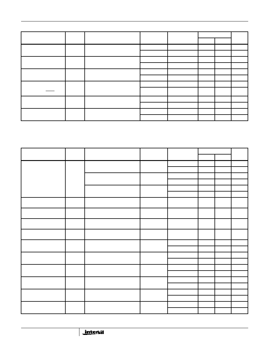
TABLE 2. AC ELECTRICAL PERFORMANCE CHARACTERISTICS
PARAMETER
SYMBOL
CONDITIONS (NOTE 1, 2)
GROUP A
SUBGROUPS
TEMPERATURE
LIMITS
UNITS
MIN
MAX
Propagation Delay
Clock to Q
TPHL1
TPLH1
VDD = 5V, VIN = VDD or GND
9
+25
o
C
-
400
ns
10, 11
+125
o
C, -55
o
C
-
540
ns
Propagation Delay
Clock to COut
TPHL2
TPLH2
VDD = 5V, VIN = VDD or GND
9
+25
o
C
-
450
ns
10, 11
+125
o
C, -55
o
C
-
608
ns
Propagation Delay
TE to COut
TPHL3
TPLH3
VDD = 5V, VIN = VDD or GND
9
+25
o
C
-
250
ns
10, 11
+125
o
C, -55
o
C
-
338
ns
Propagation Delay
CD40160BMS,
CD40161BMS Clear to Q
TPHL4
VDD = 5V, VIN = VDD or GND
9
+25
o
C
-
500
ns
10, 11
+125
o
C, -55
o
C
-
675
ns
Transition Time
TTHL
TTLH
VDD = 5V, VIN = VDD or GND
9
+25
o
C
-
200
ns
10, 11
+125
o
C, -55
o
C
-
270
ns
Maximum Clock Input Fre-
quency
FCL
VDD = 5V, VIN = VDD or GND
9
+25
o
C
2
-
MHz
10, 11
+125
o
C, -55
o
C
1.48
-
MHz
NOTES:
1. CL = 50pF, RL = 200K, Input TR, TF < 20ns.
2. -55
o
C and +125
o
C limits guaranteed, 100% testing being implemented.
TABLE 3. ELECTRICAL PERFORMANCE CHARACTERISTICS
PARAMETER
SYMBOL
CONDITIONS
NOTES
TEMPERATURE
LIMITS
UNITS
MIN
MAX
Supply Current
IDD
VDD = 5V, VIN = VDD or GND
1, 2
-55
o
C, +25
o
C
-
5
�
A
+125
o
C
-
150
�
A
VDD = 10V, VIN = VDD or GND
1, 2
-55
o
C, +25
o
C
-
10
�
A
+125
o
C
-
300
�
A
VDD = 15V, VIN = VDD or GND
1, 2
-55
o
C, +25
o
C
-
10
�
A
+125
o
C
-
600
�
A
Output Voltage
VOL
VDD = 5V, No Load
1, 2
+25
o
C, +125
o
C, -
55
o
C
-
50
mV
Output Voltage
VOL
VDD = 10V, No Load
1, 2
+25
o
C, +125
o
C, -
55
o
C
-
50
mV
Output Voltage
VOH
VDD = 5V, No Load
1, 2
+25
o
C, +125
o
C, -
55
o
C
4.95
-
V
Output Voltage
VOH
VDD = 10V, No Load
1, 2
+25
o
C, +125
o
C, -
55
o
C
9.95
-
V
Output Current (Sink)
IOL5
VDD = 5V, VOUT = 0.4V
1, 2
+125
o
C
0.36
-
mA
-55
o
C
0.64
-
mA
Output Current (Sink)
IOL10
VDD = 10V, VOUT = 0.5V
1, 2
+125
o
C
0.9
-
mA
-55
o
C
1.6
-
mA
Output Current (Sink)
IOL15
VDD = 15V, VOUT = 1.5V
1, 2
+125
o
C
2.4
-
mA
-55
o
C
4.2
-
mA
Output Current (Source)
IOH5A
VDD = 5V, VOUT = 4.6V
1, 2
+125
o
C
-
-0.36
mA
-55
o
C
-
-0.64
mA
Output Current (Source)
IOH5B
VDD = 5V, VOUT = 2.5V
1, 2
+125
o
C
-
-1.15
mA
-55
o
C
-
-2.0
mA
Output Current (Source)
IOH10
VDD = 10V, VOUT = 9.5V
1, 2
+125
o
C
-
-0.9
mA
-55
o
C
-
-1.6
mA
CD40160BMS, CD40161BMS, CD40162BMS, CD40163BMS
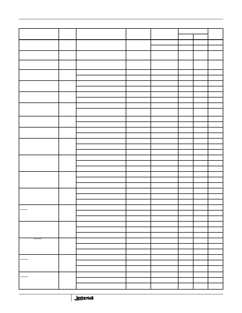
4-4
Output Current (Source)
IOH15
VDD =15V, VOUT = 13.5V
1, 2
+125
o
C
-
-2.4
mA
-55
o
C
-
-4.2
mA
Input Voltage Low
VIL
VDD = 10V, VOH > 9V, VOL < 1V
1, 2
+25
o
C, +125
o
C, -
55
o
C
-
3
V
Input Voltage High
VIH
VDD = 10V, VOH > 9V, VOL < 1V
1, 2
+25
o
C, +125
o
C, -
55
o
C
7
-
V
Propagation Delay
Clock to Q
TPHL1
TPLH1
VDD = 10V
1, 2, 3
+25
o
C
-
160
ns
VDD = 15V
1, 2, 3
+25
o
C
-
120
ns
Propagation Delay
Clock to C Out
TPHL2
TPLH2
VDD = 10V
1, 2, 3
+25
o
C
-
190
ns
VDD = 15V
1, 2, 3
+25
o
C
-
140
ns
Propagation Delay
TE to C Out
TPHL3
TPLH3
VDD = 10V
1, 2, 3
+25
o
C
-
110
ns
VDD = 15V
1, 2, 3
+25
o
C
-
80
ns
Propagation Delay
CD40160BMS,
CD40161BMS Clear to Q
TPHL4
VDD = 10V
1, 2, 3
+25
o
C
-
220
ns
VDD = 15V
1, 2, 3
+25
o
C
-
160
ns
Transition Time
TTHL
TTLH
VDD = 10V
1, 2, 3
+25
o
C
-
100
ns
VDD = 15V
1, 2, 3
+25
o
C
-
80
ns
Maximum Clock Input Fre-
quency
FCL
VDD = 10V
1, 2, 3
+25
o
C
5.5
-
MHz
VDD = 15V
1, 2, 3
+25
o
C
8
-
MHz
Maximum Clock Rise or
Fall Time
TRCL
TFCL
VDD = 5V
1, 2, 3, 4
+25
o
C
-
200
�
s
VDD = 10V
1, 2, 3, 4
+25
o
C
-
70
�
s
VDD = 15V
1, 2, 3, 4
+25
o
C
-
15
�
s
Minimum Data Hold Time
Clock Operation
TH
VDD = 5V
1, 2, 3
+25
o
C
-
0
ns
VDD = 10V
1, 2, 3
+25
o
C
-
0
ns
VDD = 15V
1, 2, 3
+25
o
C
-
0
ns
Minimum Clock Pulse
Width
Clock Operation
TW
VDD = 5V
1, 2, 3
+25
o
C
-
170
ns
VDD = 10V
1, 2, 3
+25
o
C
-
70
ns
VDD = 15V
1, 2, 3
+25
o
C
-
50
ns
Minimum Setup Time
Data to Clock
TS
VDD = 5V
1, 2, 3
+25
o
C
-
240
ns
VDD = 10V
1, 2, 3
+25
o
C
-
90
ns
VDD = 15V
1, 2, 3
+25
o
C
-
60
ns
Minimum Setup Time
Load to Clock
TS
VDD = 5V
1, 2, 3
+25
o
C
-
240
ns
VDD = 10V
1, 2, 3
+25
o
C
-
90
ns
VDD = 15V
1, 2, 3
+25
o
C
-
60
ns
Minimum Setup Time PE
to TE to Clock
TS
VDD = 5V
1, 2, 3
+25
o
C
-
340
ns
VDD = 10V
1, 2, 3
+25
o
C
-
140
ns
VDD = 15V
1, 2, 3
+25
o
C
-
100
ns
Minimum Clear Pulse
Width (CD40160BMS,
CD40161BMS)
TW
VDD = 5V
1, 2, 3
+25
o
C
-
170
ns
VDD = 10V
1, 2, 3
+25
o
C
-
70
ns
VDD = 15V
1, 2, 3
+25
o
C
-
50
ns
Minimum Setup Time
Clear to Clock
(CD40162BMS,
CD40163BMS)
TS
VDD = 5V
1, 2, 3
+25
o
C
-
340
ns
VDD = 10V
1, 2, 3
+25
o
C
-
140
ns
VDD = 15V
1, 2, 3
+25
o
C
-
100
ns
Minimum Hold Time
Clear to Clock
(CD40162BMS,
CD40163BMS)
TH
VDD = 5V
1, 2, 3
+25
o
C
-
0
ns
VDD = 10V
1, 2, 3
+25
o
C
-
0
ns
VDD = 15V
1, 2, 3
+25
o
C
-
0
ns
TABLE 3. ELECTRICAL PERFORMANCE CHARACTERISTICS (Continued)
PARAMETER
SYMBOL
CONDITIONS
NOTES
TEMPERATURE
LIMITS
UNITS
MIN
MAX
CD40160BMS, CD40161BMS, CD40162BMS, CD40163BMS
4-5
Minimum Clear Removal
Time
(CD40160BMS,
CD40161BMS)
TREM
VDD = 5V
1, 2, 3
+25
o
C
-
200
ns
VDD = 10V
1, 2, 3
+25
o
C
-
100
ns
VDD = 15V
1, 2, 3
+25
o
C
-
70
ns
NOTES:
1. All voltages referenced to device GND.
2. The parameters listed on Table 3 are controlled via design or process and are not directly tested. These parameters are characterized on initial
design release and upon design changes which would affect these characteristics.
3. CL = 50pF, RL = 200K, Input TR, TF < 20ns.
4. If more than one unit is cascaded, TRCL should be made less than or equal to the sumof the transition time and the fixed propagation delay of
the output of the driving stage for the estimated capacitive load.
TABLE 4. POST IRRADIATION ELECTRICAL PERFORMANCE CHARACTERISTICS
PARAMETER
SYMBOL
CONDITIONS
NOTES
TEMPERATURE
LIMITS
UNITS
MIN
MAX
Supply Current
IDD
VDD = 20V, VIN = VDD or GND
1, 4
+25
o
C
-
25
�
A
N Threshold Voltage
VNTH
VDD = 10V, ISS = -10
�
A
1, 4
+25
o
C
-2.8
-0.2
V
N Threshold Voltage Delta
VTN
VDD = 10V, ISS = -10
�
A
1, 4
+25
o
C
-
�
1
V
P Threshold Voltage
VTP
VSS = 0V, IDD = 10
�
A
1, 4
+25
o
C
0.2
2.8
V
P Threshold Voltage Delta
VTP
VSS = 0V, IDD = 10
�
A
1, 4
+25
o
C
-
�
1
V
Functional
F
VDD = 18V, VIN = VDD or GND
1
+25
o
C
VOH >
VDD/2
VOL <
VDD/2
V
VDD = 3V, VIN = VDD or GND
Propagation Delay Time
TPHL
TPLH
VDD = 5V
1, 2, 3, 4
+25
o
C
-
1.35 x
+25
o
C
Limit
ns
NOTES: 1. All voltages referenced to device GND.
2. CL = 50pF, RL = 200K, Input TR, TF < 20ns.
3. See Table 2 for +25
o
C limit.
4. Read and Record
TABLE 5. BURN-IN AND LIFE TEST DELTA PARAMETERS +25
o
C
PARAMETER
SYMBOL
DELTA LIMIT
Supply Current - MSI-2
IDD
�
1.0
�
A
Output Current (Sink)
IOL5
�
20% x Pre-Test Reading
Output Current (Source)
IOH5A
�
20% x Pre-Test Reading
TABLE 6. APPLICABLE SUBGROUPS
CONFORMANCE GROUP
MIL-STD-883
METHOD
GROUP A SUBGROUPS
READ AND RECORD
Initial Test (Pre Burn-In)
100% 5004
1, 7, 9
IDD, IOL5, IOH5A
Interim Test 1 (Post Burn-In)
100% 5004
1, 7, 9
IDD, IOL5, IOH5A
Interim Test 2 (Post Burn-In)
100% 5004
1, 7, 9
IDD, IOL5, IOH5A
PDA (Note 1)
100% 5004
1, 7, 9, Deltas
Interim Test 3 (Post Burn-In)
100% 5004
1, 7, 9
IDD, IOL5, IOH5A
PDA (Note 1)
100% 5004
1, 7, 9, Deltas
Final Test
100% 5004
2, 3, 8A, 8B, 10, 11
Group A
Sample 5005
1, 2, 3, 7, 8A, 8B, 9, 10, 11
Group B
Subgroup B-5
Sample 5005
1, 2, 3, 7, 8A, 8B, 9, 10, 11, Deltas
Subgroups 1, 2, 3, 9, 10, 11
Subgroup B-6
Sample 5005
1, 7, 9
Group D
Sample 5005
1, 2, 3, 8A, 8B, 9
Subgroups 1, 2 3
NOTE: 1. 5% Parameteric, 3% Functional; Cumulative for Static 1 and 2.
TABLE 3. ELECTRICAL PERFORMANCE CHARACTERISTICS (Continued)
PARAMETER
SYMBOL
CONDITIONS
NOTES
TEMPERATURE
LIMITS
UNITS
MIN
MAX
CD40160BMS, CD40161BMS, CD40162BMS, CD40163BMS