 | –≠–ª–µ–∫—Ç—Ä–æ–Ω–Ω—ã–π –∫–æ–º–ø–æ–Ω–µ–Ω—Ç: CD40181 | –°–∫–∞—á–∞—Ç—å:  PDF PDF  ZIP ZIP |
7-1400
CAUTION: These devices are sensitive to electrostatic discharge; follow proper IC Handling Procedures.
1-888-INTERSIL or 321-724-7143 | Copyright © Intersil Corporation 1999
CD40181BMS
CMOS 4 Bit Arithmetic Logic Unit
Description
The CD40181BMS is a low power four bit parallel arithmetic
logic unit (ALU) capable of providing 16 binary arithmetic
operations on two four-bit words and 16 logical functions of
two Boolean variables. The mode control input M selects
logical (M = High) or arithmetic (M = Low) operation. The
four select inputs (S0, S1, S2, and S3) select the desired
logical or arithmetic functions, which include AND, OR,
NAND, NOR and exclusive-OR and-NOR in the logic mode,
and addition, subtraction, decrement, left-shift and straight
transfer in the arithmetic mode, according to the truth table.
The CD40181BMS operation may be interpreted with either
active-low or active-high data at the A and B word inputs and
the function outputs F, by using the appropriate truth table.
The CD40181BMS contains logic for full look ahead carry
operation for fast carry generation using the carry-generate
and carry-propagate outputs G and P for the four bits of the
CD40181BMS. Use of the CD40182BMS look-ahead carry
generator in conjunction with multiple CD40181BMS's
permits high speed arithmetic operations on long words. A
ripple carry output Cn+4 is available for use in systems
where speed is not of primary importance.
Also included in the CD40181BMS is a comparator output
A = B, which assumes a high level whenever the two four-bit
input words A and B are equal and the device is in the
subtract mode. In addition, relative magnitude information
may be derived from the carry-in input Cn and ripple carry-
out output Cn+4 by placing the unit in the subtract mode and
externally decoding using the information in Table B.
The CD40181BMS is similar to industry types MC14581 and
74181.
The CD40181BMS is supplied in these 24-lead outline
packages:
Braze Seal DIP
HNZ
Ceramic Flatpack
H4P
Features
∑ High Voltage Type (20V Rating)
∑ Full Look Ahead Carry for Speed Operations on Long
Words
∑ Generates 16 Logic Functions of Two Boolean Variables
∑ Generates 16 Arithmetic Functions of Two 4 Bit Binary
Words
∑ A = B comparator Output Available
∑ Ripple Carry Input and Output Available
∑ Typical Addition Time 200ns at VDD = 10V
∑ 100% Tested for Quiescent Current at 20V
∑ 5V, 10V and 15V Parametric Ratings
∑ Maximum Input Current of 1
µ
A at 18V Over Full Pack-
age Temperature Range; 100nA at 18V and +25
o
C
∑ Noise Margin (Over Full Package/Temperature Range)
- 1V at VDD = 5V
- 2V at VDD = 10V
- 2.5V at VDD = 15V
∑ Standardized Symmetrical Output Characteristics
∑ Meets All Requirements of JEDEC Tentative Standard
No. 13B, "Standard Specifications for Description of
`B' Series CMOS Devices"
Applications
∑ Parallel Arithmetic Units
∑ Process Controllers
∑ Low Power Minicomputers
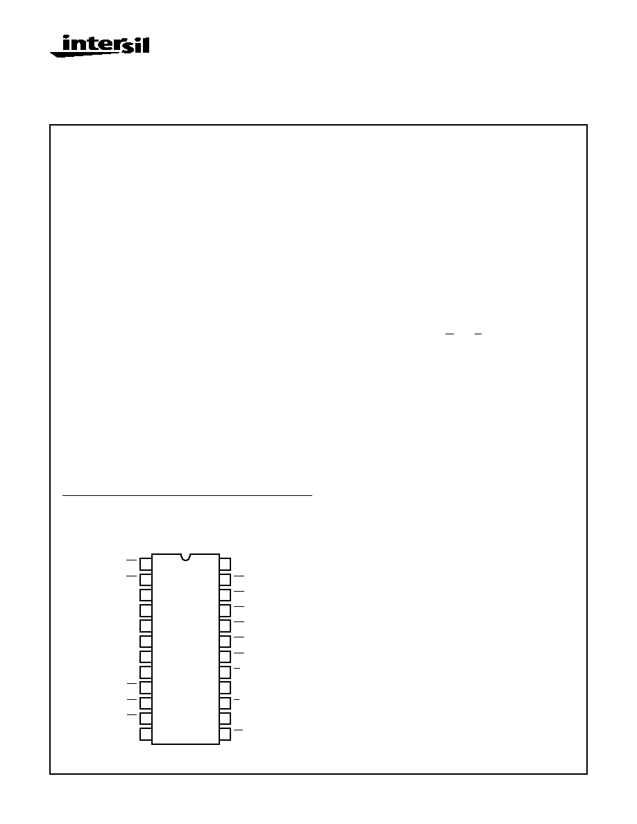
Pinout
CD40181BMS ACTIVE-LOW DATA
TOP VIEW
1
2
3
4
5
6
7
8
9
10
11
12
B0
A0
S3
S2
S1
S0
Cn
M
F0
F1
F2
VSS
16
17
18
19
20
21
22
23
24
15
14
13
VDD
B1
A2
B2
A3
G
P
A = B
F3
A1
B3
Cn+4
December 1992
File Number
3361
7-1401
CD40181BMS
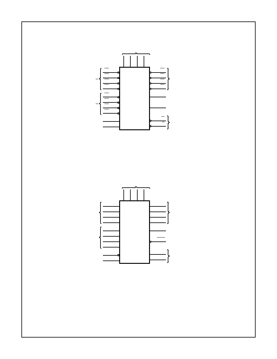
Functional Diagrams
ACTIVE-LOW DATA
ACTIVE-HIGH DATA
A0
2
A1
23
A2
21
A3
19
B0
1
B1
22
B2
20
B3
18
Cn
7
M
8
6
S0
5
S1
4
S2
3
S3
FUNCTION SELECT
INPUTS
WORD
A
WORD
B
CARRY IN
MODE
CONTROL
F0
9
F1
10
F2
11
F3
13
OUTPUT
FUNCTION
14
A = B
16
Cn+4
G
17
P
15
COMPARE
OUT
RIPPLE
CARRY OUT
LOOK AHEAD
CARRY
OUTPUTS
VDD = 24
VSS = 12
A0
2
A1
23
A2
21
A3
19
B0
1
B1
22
B2
20
B3
18
Cn
7
M
8
6
S0
5
S1
4
S2
3
S3
FUNCTION SELECT
INPUTS
WORD
A
WORD
B
CARRY IN
MODE
CONTROL
F0
9
F1
10
F2
11
F3
13
OUTPUT
FUNCTION
14
A = B
16
Cn+4
G
17
P
15
COMPARE
OUT
RIPPLE
CARRY OUT
LOOK AHEAD
CARRY
OUTPUTS
VDD = 24
VSS = 12
7-1402
Specifications CD40181BMS
Absolute Maximum Ratings
Reliability Information
DC Supply Voltage Range, (VDD) . . . . . . . . . . . . . . . -0.5V to +20V
(Voltage Referenced to VSS Terminals)
Input Voltage Range, All Inputs . . . . . . . . . . . . .-0.5V to VDD +0.5V
DC Input Current, Any One Input
. . . . . . . . . . . . . . . . . . . . . . . .±
10mA
Operating Temperature Range . . . . . . . . . . . . . . . . -55
o
C to +125
o
C
Package Types D, F, K, H
Storage Temperature Range (TSTG) . . . . . . . . . . . -65
o
C to +150
o
C
Lead Temperature (During Soldering) . . . . . . . . . . . . . . . . . +265
o
C
At Distance 1/16
±
1/32 Inch (1.59mm
±
0.79mm) from case for
10s Maximum
Thermal Resistance
ja
jc
Ceramic DIP and FRIT Package . . . . .
80
o
C/W
20
o
C/W
Flatpack Package . . . . . . . . . . . . . . . .
70
o
C/W
20
o
C/W
Maximum Package Power Dissipation (PD) at +125
o
C
For T
A
= -55
o
C to +100
o
C (Package Type D, F, K) . . . . . . 500mW
For T
A
= +100
o
C to +125
o
C (Package Type D, F, K). . . . . . Derate
Linearity at 12mW/
o
C to 200mW
Device Dissipation per Output Transistor . . . . . . . . . . . . . . . 100mW
For T
A
= Full Package Temperature Range (All Package Types)
Junction Temperature . . . . . . . . . . . . . . . . . . . . . . . . . . . . . . +175
o
C
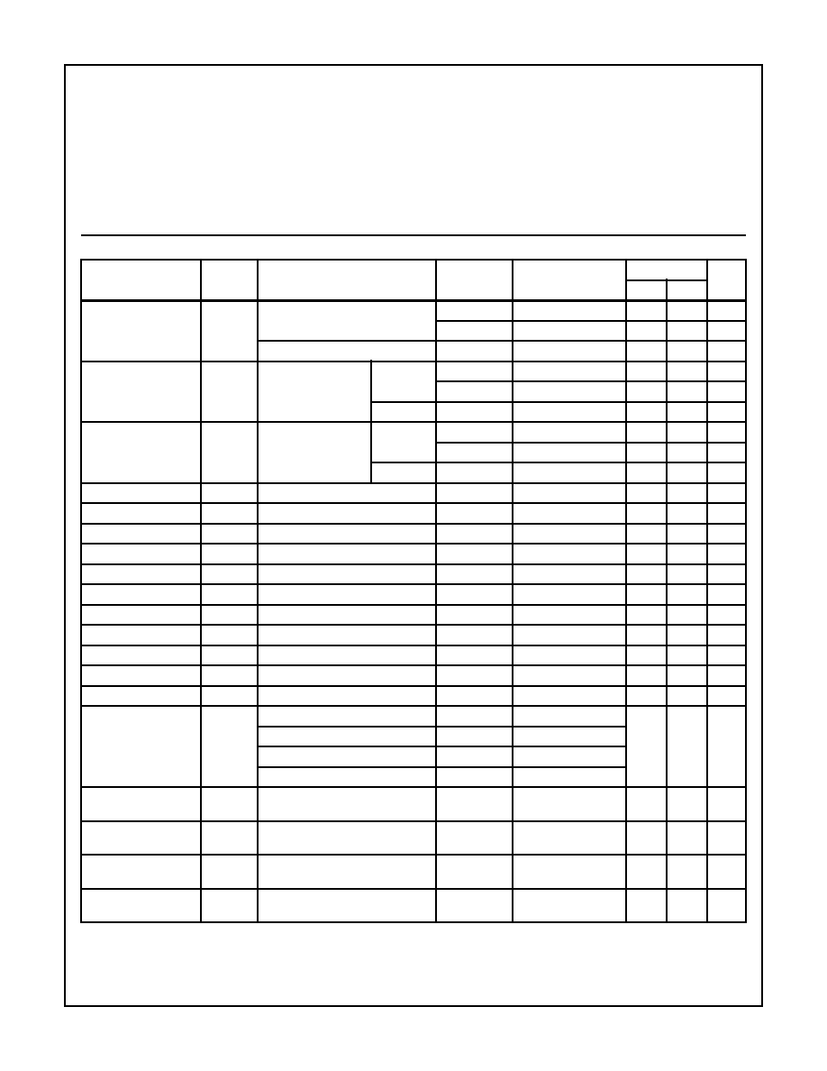
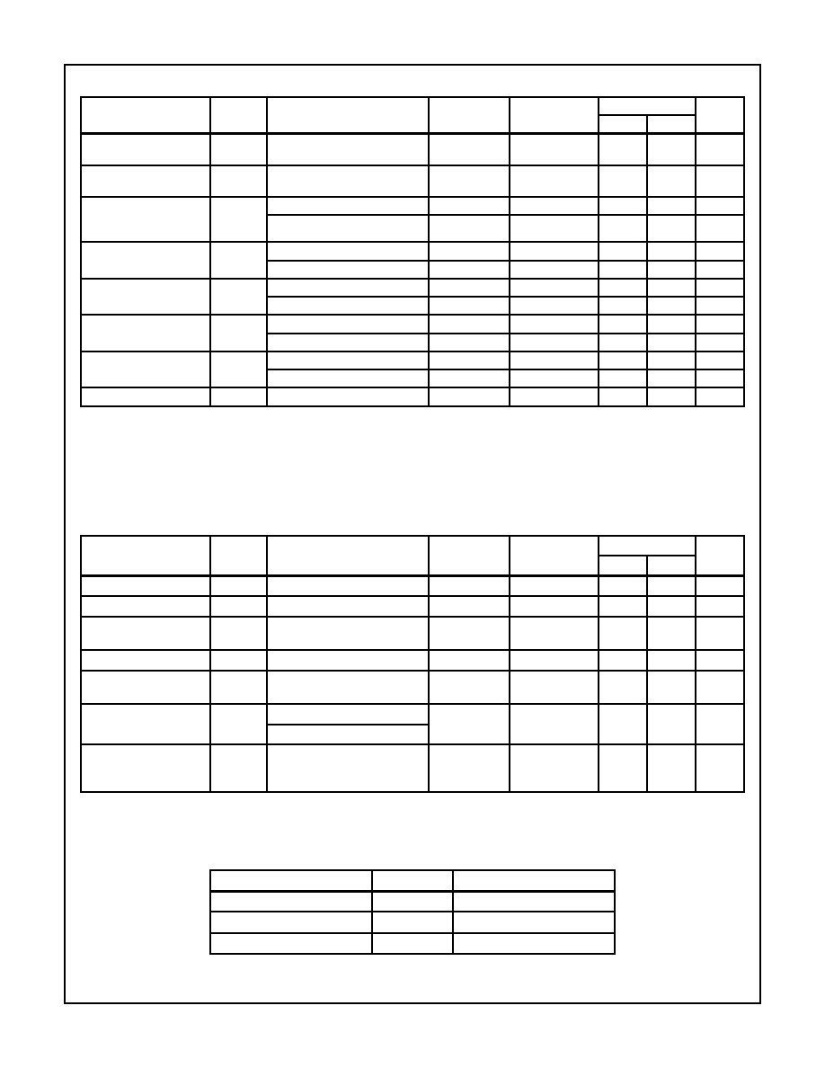
TABLE 1. DC ELECTRICAL PERFORMANCE CHARACTERISTICS
PARAMETER
SYMBOL
CONDITIONS (NOTE 1)
GROUP A
SUBGROUPS
TEMPERATURE
LIMITS
UNITS
MIN
MAX
Supply Current
IDD
VDD = 20V, VIN = VDD or GND
1
+25
o
C
-
10
µ
A
2
+125
o
C
-
1000
µ
A
VDD = 18V, VIN = VDD or GND
3
-55
o
C
-
10
µ
A
Input Leakage Current
IIL
VIN = VDD or GND
VDD = 20
1
+25
o
C
-100
-
nA
2
+125
o
C
-1000
-
nA
VDD = 18V
3
-55
o
C
-100
-
nA
Input Leakage Current
IIH
VIN = VDD or GND
VDD = 20
1
+25
o
C
-
100
nA
2
+125
o
C
-
1000
nA
VDD = 18V
3
-55
o
C
-
100
nA
Output Voltage
VOL15
VDD = 15V, No Load
1, 2, 3
+25
o
C, +125
o
C, -55
o
C
-
50
mV
Output Voltage
VOH15
VDD = 15V, No Load (Note 3)
1, 2, 3
+25
o
C, +125
o
C, -55
o
C 14.95
-
V
Output Current (Sink)
IOL5
VDD = 5V, VOUT = 0.4V
1
+25
o
C
0.53
-
mA
Output Current (Sink)
IOL10
VDD = 10V, VOUT = 0.5V
1
+25
o
C
1.4
-
mA
Output Current (Sink)
IOL15
VDD = 15V, VOUT = 1.5V
1
+25
o
C
3.5
-
mA
Output Current (Source)
IOH5A
VDD = 5V, VOUT = 4.6V
1
+25
o
C
-
-0.53
mA
Output Current (Source)
IOH5B
VDD = 5V, VOUT = 2.5V
1
+25
o
C
-
-1.8
mA
Output Current (Source)
IOH10
VDD = 10V, VOUT = 9.5V
1
+25
o
C
-
-1.4
mA
Output Current (Source)
IOH15
VDD = 15V, VOUT = 13.5V
1
+25
o
C
-
-3.5
mA
N Threshold Voltage
VNTH
VDD = 10V, ISS = -10
µ
A
1
+25
o
C
-2.8
-0.7
V
P Threshold Voltage
VPTH
VSS = 0V, IDD = 10
µ
A
1
+25
o
C
0.7
2.8
V
Functional
F
VDD = 2.8V, VIN = VDD or GND
7
+25
o
C
VOH >
VDD/2
VOL <
VDD/2
V
VDD = 20V, VIN = VDD or GND
7
+25
o
C
VDD = 18V, VIN = VDD or GND
8A
+125
o
C
VDD = 3V, VIN = VDD or GND
8B
-55
o
C
Input Voltage Low
(Note 2)
VIL
VDD = 5V, VOH > 4.5V, VOL < 0.5V
1, 2, 3
+25
o
C, +125
o
C, -55
o
C
-
1.5
V
Input Voltage High
(Note 2)
VIH
VDD = 5V, VOH > 4.5V, VOL < 0.5V
1, 2, 3
+25
o
C, +125
o
C, -55
o
C
3.5
-
V
Input Voltage Low
(Note 2)
VIL
VDD = 15V, VOH > 13.5V,
VOL < 1.5V
1, 2, 3
+25
o
C, +125
o
C, -55
o
C
-
4
V
Input Voltage High
(Note 2)
VIH
VDD = 15V, VOH > 13.5V,
VOL < 1.5V
1, 2, 3
+25
o
C, +125
o
C, -55
o
C
11
-
V
NOTES: 1. All voltages referenced to device GND, 100% testing being
implemented.
2. Go/No Go test with limits applied to inputs.
3. For accuracy, voltage is measured differentially to VDD. Limit
is 0.050V max.
7-1403
Specifications CD40181BMS
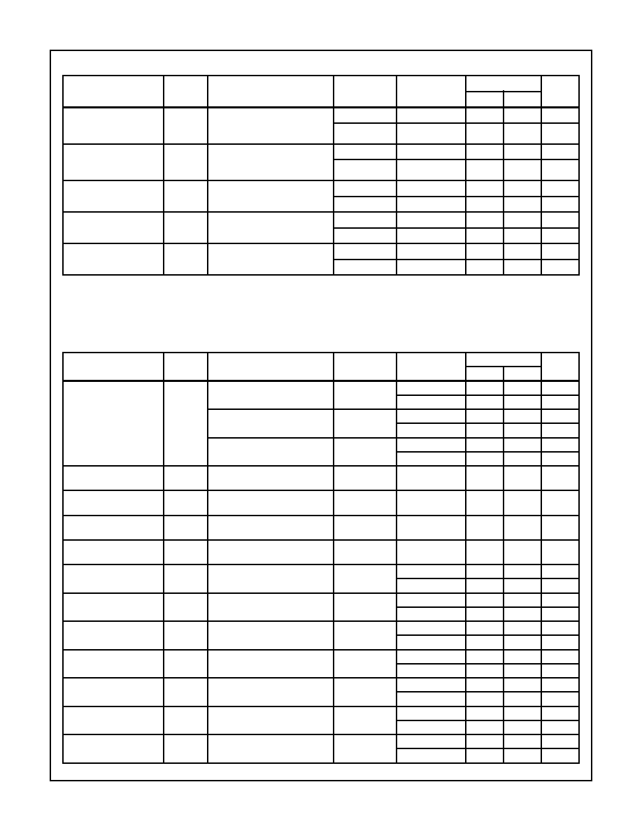
TABLE 2. AC ELECTRICAL PERFORMANCE CHARACTERISTICS
PARAMETER
SYMBOL
CONDITIONS (NOTE 1, 2)
GROUP A
SUBGROUPS
TEMPERATURE
LIMITS
UNITS
MIN
MAX
Propagation Delay
A or B to F (Logic Mode),
A or B to G or P
TPHL1
TPLH1
VDD = 5V, VIN = VDD or GND
9
+25
o
C
-
800
ns
10, 11
+125
o
C, -55
o
C
-
1080
ns
Propagation Delay
A or B to F, Cn+4, or A =
B
TPHL2
TPLH2
VDD = 5V, VIN = VDD or GND
9
+25
o
C
-
1000
ns
10, 11
+125
o
C, -55
o
C
-
1350
ns
Propagation Delay
Cn to F
TPHL3
TPLH3
VDD = 5V, VIN = VDD or GND
9
+25
o
C
-
640
ns
10, 11
+125
o
C, -55
o
C
-
864
ns
Propagation Delay
Cn to Cn+4
TPHL4
TPLH4
VDD = 5V, VIN = VDD or GND
9
+25
o
C
-
400
ns
10, 11
+125
o
C, -55
o
C
-
540
ns
Transition Time
TTHL
TTLH
VDD = 5V, VIN = VDD or GND
9
+25
o
C
-
200
ns
10, 11
+125
o
C, -55
o
C
-
270
ns
NOTES:
1. CL = 50pF, RL = 200K, Input TR, TF < 20ns.
2. -55
o
C and +125
o
C limits guaranteed, 100% testing being implemented.
TABLE 3. ELECTRICAL PERFORMANCE CHARACTERISTICS
PARAMETER
SYMBOL
CONDITIONS
NOTES
TEMPERATURE
LIMITS
UNITS
MIN
MAX
Supply Current
IDD
VDD = 5V, VIN = VDD or GND
1, 2
-55
o
C, +25
o
C
-
5
µ
A
+125
o
C
-
150
µ
A
VDD = 10V, VIN = VDD or GND
1, 2
-55
o
C, +25
o
C
-
10
µ
A
+125
o
C
-
300
µ
A
VDD = 15V, VIN = VDD or GND
1, 2
-55
o
C, +25
o
C
-
10
µ
A
+125
o
C
-
600
µ
A
Output Voltage
VOL
VDD = 5V, No Load
1, 2
+25
o
C, +125
o
C,
-55
o
C
-
50
mV
Output Voltage
VOL
VDD = 10V, No Load
1, 2
+25
o
C, +125
o
C,
-55
o
C
-
50
mV
Output Voltage
VOH
VDD = 5V, No Load
1, 2
+25
o
C, +125
o
C,
-55
o
C
4.95
-
V
Output Voltage
VOH
VDD = 10V, No Load
1, 2
+25
o
C, +125
o
C,
-55
o
C
9.95
-
V
Output Current (Sink)
IOL5
VDD = 5V, VOUT = 0.4V
1, 2
+125
o
C
0.36
-
mA
-55
o
C
0.64
-
mA
Output Current (Sink)
IOL10
VDD = 10V, VOUT = 0.5V
1, 2
+125
o
C
0.9
-
mA
-55
o
C
1.6
-
mA
Output Current (Sink)
IOL15
VDD = 15V, VOUT = 1.5V
1, 2
+125
o
C
2.4
-
mA
-55
o
C
4.2
-
mA
Output Current (Source)
IOH5A
VDD = 5V, VOUT = 4.6V
1, 2
+125
o
C
-
-0.36
mA
-55
o
C
-
-0.64
mA
Output Current (Source)
IOH5B
VDD = 5V, VOUT = 2.5V
1, 2
+125
o
C
-
-1.15
mA
-55
o
C
-
-2.0
mA
Output Current (Source)
IOH10
VDD = 10V, VOUT = 9.5V
1, 2
+125
o
C
-
-0.9
mA
-55
o
C
-
-1.6
mA
Output Current (Source)
IOH15
VDD =15V, VOUT = 13.5V
1, 2
+125
o
C
-
-2.4
mA
-55
o
C
-
-4.2
mA
7-1404
Specifications CD40181BMS
Input Voltage Low
VIL
VDD = 10V, VOH > 9V, VOL < 1V
1, 2
+25
o
C, +125
o
C,
-55
o
C
-
3
V
Input Voltage High
VIH
VDD = 10V, VOH > 9V, VOL < 1V
1, 2
+25
o
C, +125
o
C,
-55
o
C
+7
-
V
Propagation Delay
A or B to F (Logic Mode)
A or B to G or P
TPHL1
TPLH1
VDD = 10V
1, 2, 3
+25
o
C
-
320
ns
VDD = 15V
1, 2, 3
+25
o
C
-
240
ns
Propagation Delay
A or B to F, Cn+4 or A = B
TPHL2
TPLH2
VDD = 10V
1, 2, 3
+25
o
C
-
400
ns
VDD = 15V
1, 2, 3
+25
o
C
-
280
ns
Propagation Delay
Cn to F
TPHL3
TPLH3
VDD = 10V
1, 2, 3
+25
o
C
-
270
ns
VDD = 15V
1, 2, 3
+25
o
C
-
200
ns
Propagation Delay
Cn to Cn+4
TPHL4
TPLH4
VDD = 10V
1, 2, 3
+25
o
C
-
200
ns
VDD = 15V
1, 2, 3
+25
o
C
-
140
ns
Transition Time
TTHL
TTLH
VDD = 10V
1, 2, 3
+25
o
C
-
100
ns
VDD = 15V
1, 2, 3
+25
o
C
-
80
ns
Input Capacitance
CIN
Any Input
1, 2
+25
o
C
-
7.5
pF
NOTES:
1. All voltages referenced to device GND.
2. The parameters listed on Table 3 are controlled via design or process and are not directly tested. These parameters are characterized
on initial design release and upon design changes which would affect these characteristics.
3. CL = 50pF, RL = 200K, Input TR, TF < 20ns.
TABLE 4. POST IRRADIATION ELECTRICAL PERFORMANCE CHARACTERISTICS
PARAMETER
SYMBOL
CONDITIONS
NOTES
TEMPERATURE
LIMITS
UNITS
MIN
MAX
Supply Current
IDD
VDD = 20V, VIN = VDD or GND
1, 4
+25
o
C
-
25
µ
A
N Threshold Voltage
VNTH
VDD = 10V, ISS = -10
µ
A
1, 4
+25
o
C
-2.8
-0.2
V
N Threshold Voltage
Delta
VTND
VDD = 10V, ISS = -10
µ
A
1, 4
+25
o
C
-
±
1
V
P Threshold Voltage
VTP
VSS = 0V, IDD = 10
µ
A
1, 4
+25
o
C
0.2
2.8
V
P Threshold Voltage
Delta
VTPD
VSS = 0V, IDD = 10
µ
A
1, 4
+25
o
C
-
±
1
V
Functional
F
VDD = 18V, VIN = VDD or GND
1
+25
o
C
VOH >
VDD/2
VOL <
VDD/2
V
VDD = 3V, VIN = VDD or GND
Propagation Delay Time
TPHL
TPLH
VDD = 5V
1, 2, 3, 4
+25
o
C
-
1.35 x
+25
o
C
Limit
ns
NOTES: 1. All voltages referenced to device GND.
2. CL = 50pF, RL = 200K, Input TR, TF < 20ns.
3. See Table 2 for +25
o
C limit.
4. Read and Record
TABLE 5. BURN-IN AND LIFE TEST DELTA PARAMETERS +25
o
C
PARAMETER
SYMBOL
DELTA LIMIT
Supply Current - MSI-2
IDD
±
1.0
µ
A
Output Current (Sink)
IOL5
±
20% x Pre-Test Reading
Output Current (Source)
IOH5A
±
20% x Pre-Test Reading
TABLE 3. ELECTRICAL PERFORMANCE CHARACTERISTICS
(Continued)
PARAMETER
SYMBOL
CONDITIONS
NOTES
TEMPERATURE
LIMITS
UNITS
MIN
MAX