7-798
CAUTION: These devices are sensitive to electrostatic discharge; follow proper IC Handling Procedures.
1-888-INTERSIL or 321-724-7143 | Copyright © Intersil Corporation 1999
CD4029BMS
CMOS Presettable Up/Down Counter
Description
CD4029BMS consists of a four-stage binary or BCD-decade up/
down counter with provisions for look-ahead carry in both count-
ing modes. The inputs consist of a single CLOCK, CARRY-IN
(CLOCK ENABLE), BINARY/DECADE, UP/DOWN, PRESET
ENABLE, and four individual JAM signals. Q1, Q2, Q3, Q4 and a
CARRY OUT signal are provided as outputs.
A high PRESET ENABLE signal allows information on the JAM
INPUTS to preset the counter to any state asynchronously with
the clock. A low on each JAM line, when the PRESET-ENABLE
signal is high, resets the counter to its zero count. The counter is
advanced one count at the positive transition of the clock when
the CARRY-IN and PRE-SET ENABLE signals are low.
Advancement is inhibited when the CARRY-IN or PRESET
ENABLE signals are high. The CARRY-OUT signal is normally
high and goes low when the counter reaches its maximum count
in the UP mode or the minimum count in the DOWN mode pro-
vided the CARRY-IN signal is low. The CARRY-IN signal in the
low state can thus be considered a CLOCK ENABLE. The
CARRY-IN terminal must be connected to VSS when not in use.
Binary counting is accomplished when the BINARY/DECADE
input is high; the counter counts in the decade mode when the
BINARY/DECADE input is low. The counter counts up when the
UP/DOWN input is high, and down when the UP/DOWN input is
low. Multiple packages can be connected in either a parallel-
clocking or a ripple-clocking arrangement as shown in Figure 17.
Parallel clocking provides synchronous control and hence faster
response from all counting outputs. Ripple-clocking allows for
longer clock input rise and fall times.
The CD4029BMS is supplied in these 16-lead outline packages:
Braze Seal DIP
H4X
Frit Seal DIP
H1F
Ceramic Flatpack H6W
Features
∑ High-Voltage Type (20V Rating)
∑ Medium Speed Operation: 8MHz (Typ.) at CL = 50pF
and VDD - VSS = 10V
∑ Multi-Package Parallel Clocking for Synchronous High
Speed Output Response or Ripple Clocking for Slow
Clock Input Rise and Fall Times
∑ "Preset Enable" and Individual "Jam" Inputs Provided
∑ Binary or Decade Up/Down Counting
∑ BCD Outputs in Decade Mode
∑ 100% Tested for Maximum Quiescent Current at 20V
∑ 5V, 10V and 15V Parametric Ratings
∑ Standardized Symmetrical Output Characteristics
∑ Maximum Input Current of 1
µ
A at 18V Over Full Pack-
age-Temperature Range; 100nA at 18V and +25
o
C
∑ Noise Margin (Over Full Package Temperature Range):
- 1V at VDD = 5V
- 2V at VDD = 10V
- 2.5V at VDD = 15V
∑ Meets All Requirements of JEDEC Tentative Stan-
dards No. 13B, "Standard Specifications for Descrip-
tion of "B" Series CMOS Device's
Applications
∑ Programmable Binary and Decade Counting/Fre-
quency Synthesizers-BCD Output
∑ Analog to Digital and Digital to Analog Conversion
∑ Up/Down Binary Counting
∑ Difference Counting
∑ Magnitude and Sign Generation
∑ Up/Down Decade Counting
December 1992
File Number
3304
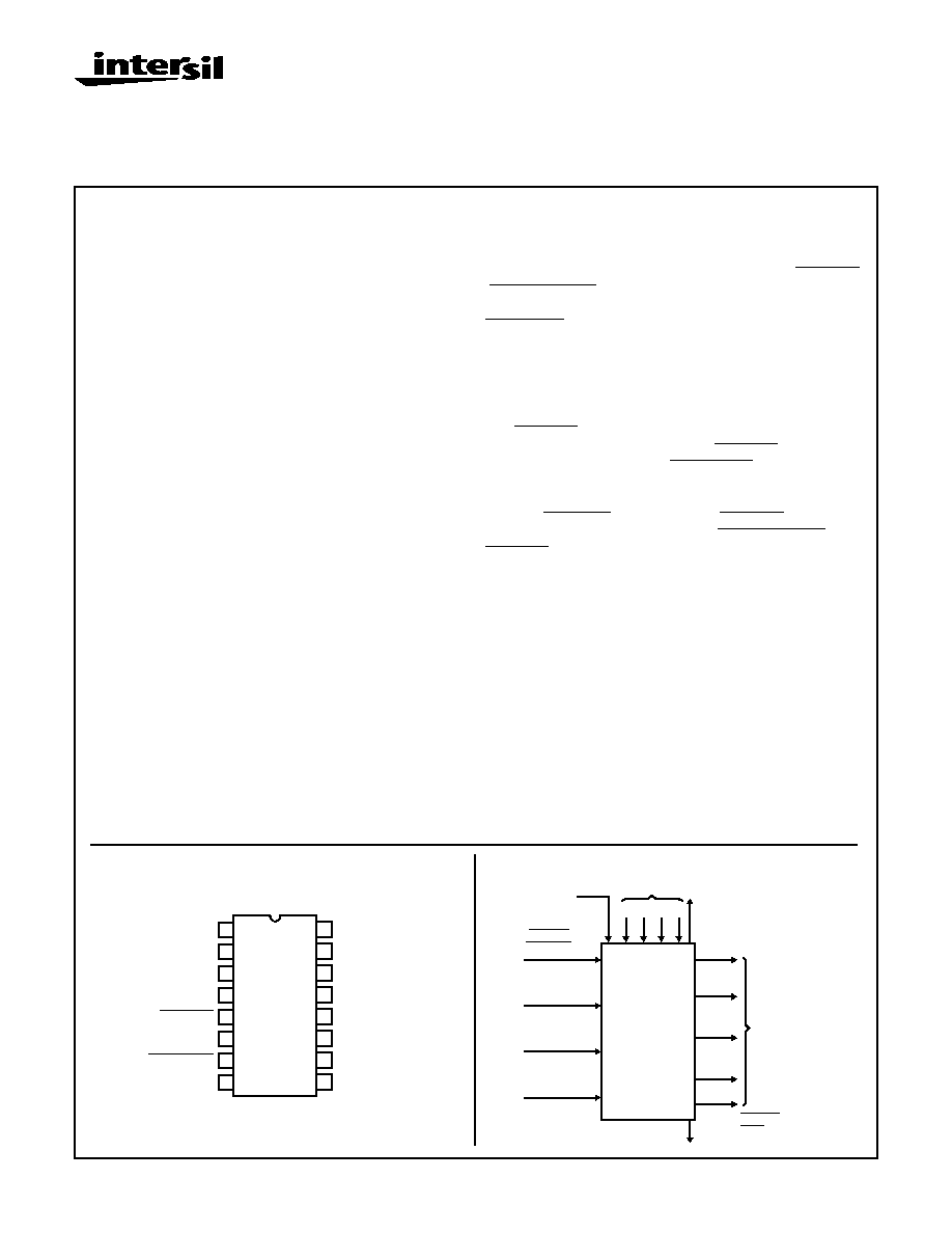
Pinout
CD4029BMS
TOP VIEW
14
15
16
9
13
12
11
10
1
2
3
4
5
7
6
8
PRESET ENABLE
Q4
JAM 4
JAM 1
CARRY IN
Q1
VSS
CARRY OUT
VDD
Q3
JAM 3
JAM 2
Q2
UP/DOWN
BINARY/DECADE
CLOCK
Functional Diagram
13
12
16
PRESET
ENABLE
1
4
3
1
2
3
4
JAM INPUTS
VDD
CARRY IN
(CLOCK
ENABLE)
5
9
10
15
BINARY/
DECADE
UP/DOWN
CLOCK
8
VSS
7
2
14
11
6 Q1
Q2
Q3
Q4
CARRY
OUT
BUFFERED
OUTPUTS
7-799
Specifications CD4029BMS
Absolute Maximum Ratings
Reliability Information
DC Supply Voltage Range, (VDD) . . . . . . . . . . . . . . . -0.5V to +20V
(Voltage Referenced to VSS Terminals)
Input Voltage Range, All Inputs . . . . . . . . . . . . .-0.5V to VDD +0.5V
DC Input Current, Any One Input
. . . . . . . . . . . . . . . . . . . . . . . .±
10mA
Operating Temperature Range . . . . . . . . . . . . . . . . -55
o
C to +125
o
C
Package Types D, F, K, H
Storage Temperature Range (TSTG) . . . . . . . . . . . -65
o
C to +150
o
C
Lead Temperature (During Soldering) . . . . . . . . . . . . . . . . . +265
o
C
At Distance 1/16
±
1/32 Inch (1.59mm
±
0.79mm) from case for
10s Maximum
Thermal Resistance . . . . . . . . . . . . . . . .
ja
jc
Ceramic DIP and FRIT Package . . . . .
80
o
C/W
20
o
C/W
Flatpack Package . . . . . . . . . . . . . . . .
70
o
C/W
20
o
C/W
Maximum Package Power Dissipation (PD) at +125
o
C
For TA = -55
o
C to +100
o
C (Package Type D, F, K) . . . . . . 500mW
For TA = +100
o
C to +125
o
C (Package Type D, F, K) . . . . . Derate
Linearity at 12mW/
o
C to 200mW
Device Dissipation per Output Transistor . . . . . . . . . . . . . . . 100mW
For TA = Full Package Temperature Range (All Package Types)
Junction Temperature . . . . . . . . . . . . . . . . . . . . . . . . . . . . . . +175
o
C
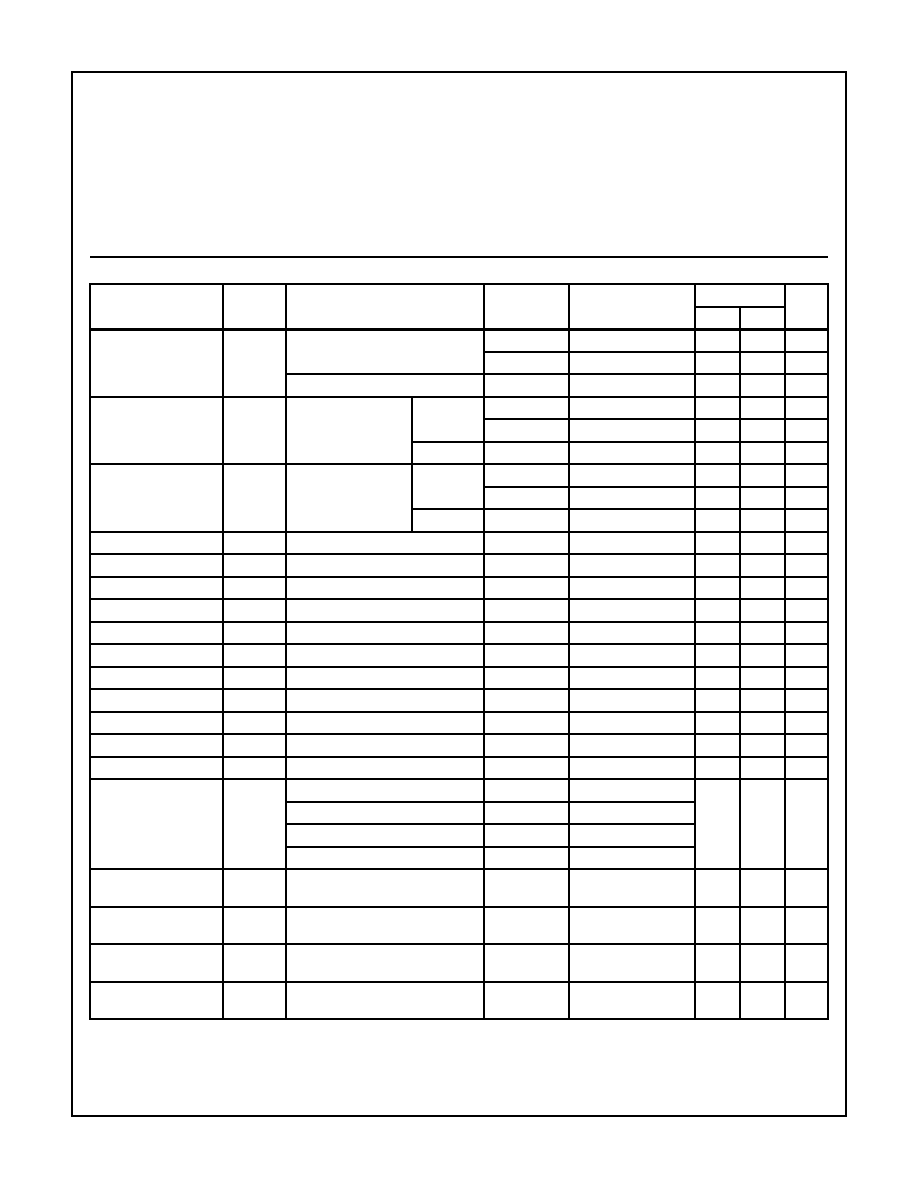
TABLE 1. DC ELECTRICAL PERFORMANCE CHARACTERISTICS
PARAMETER
SYMBOL
CONDITIONS (NOTE 1)
GROUP A
SUBGROUPS
TEMPERATURE
LIMITS
UNITS
MIN
MAX
Supply Current
IDD
VDD = 20V, VIN = VDD or GND
1
+25
o
C
-
10
µ
A
2
+125
o
C
-
1000
µ
A
VDD = 18V, VIN = VDD or GND
3
-55
o
C
-
10
µ
A
Input Leakage Current
IIL
VIN = VDD or GND
VDD = 20
1
+25
o
C
-100
-
nA
2
+125
o
C
-1000
-
nA
VDD = 18V
3
-55
o
C
-100
-
nA
Input Leakage Current
IIH
VIN = VDD or GND
VDD = 20
1
+25
o
C
-
100
nA
2
+125
o
C
-
1000
nA
VDD = 18V
3
-55
o
C
-
100
nA
Output Voltage
VOL15
VDD = 15V, No Load
1, 2, 3
+25
o
C, +125
o
C, -55
o
C
-
50
mV
Output Voltage
VOH15
VDD = 15V, No Load (Note 3)
1, 2, 3
+25
o
C, +125
o
C, -55
o
C 14.95
-
V
Output Current (Sink)
IOL5
VDD = 5V, VOUT = 0.4V
1
+25
o
C
0.53
-
mA
Output Current (Sink)
IOL10
VDD = 10V, VOUT = 0.5V
1
+25
o
C
1.4
-
mA
Output Current (Sink)
IOL15
VDD = 15V, VOUT = 1.5V
1
+25
o
C
3.5
-
mA
Output Current (Source)
IOH5A
VDD = 5V, VOUT = 4.6V
1
+25
o
C
-
-0.53
mA
Output Current (Source)
IOH5B
VDD = 5V, VOUT = 2.5V
1
+25
o
C
-
-1.8
mA
Output Current (Source)
IOH10
VDD = 10V, VOUT = 9.5V
1
+25
o
C
-
-1.4
mA
Output Current (Source)
IOH15
VDD = 15V, VOUT = 13.5V
1
+25
o
C
-
-3.5
mA
N Threshold Voltage
VNTH
VDD = 10V, ISS = -10
µ
A
1
+25
o
C
-2.8
-0.7
V
P Threshold Voltage
VPTH
VSS = 0V, IDD = 10
µ
A
1
+25
o
C
0.7
2.8
V
Functional
F
VDD = 2.8V, VIN = VDD or GND
7
+25
o
C
VOH >
VDD/2
VOL <
VDD/2
V
VDD = 20V, VIN = VDD or GND
7
+25
o
C
VDD = 18V, VIN = VDD or GND
8A
+125
o
C
VDD = 3V, VIN = VDD or GND
8B
-55
o
C
Input Voltage Low
(Note 2)
VIL
VDD = 5V, VOH > 4.5V, VOL < 0.5V
1, 2, 3
+25
o
C, +125
o
C, -55
o
C
-
1.5
V
Input Voltage High
(Note 2)
VIH
VDD = 5V, VOH > 4.5V, VOL < 0.5V
1, 2, 3
+25
o
C, +125
o
C, -55
o
C
3.5
-
V
Input Voltage Low
(Note 2)
VIL
VDD = 15V, VOH > 13.5V,
VOL < 1.5V
1, 2, 3
+25
o
C, +125
o
C, -55
o
C
-
4
V
Input Voltage High
(Note 2)
VIH
VDD = 15V, VOH > 13.5V,
VOL < 1.5V
1, 2, 3
+25
o
C, +125
o
C, -55
o
C
11
-
V
NOTES: 1. All voltages referenced to device GND, 100% testing being
implemented.
2. Go/No Go test with limits applied to inputs.
3. For accuracy, voltage is measured differentially to VDD. Limit
is 0.050V max.

7-800
Specifications CD4029BMS
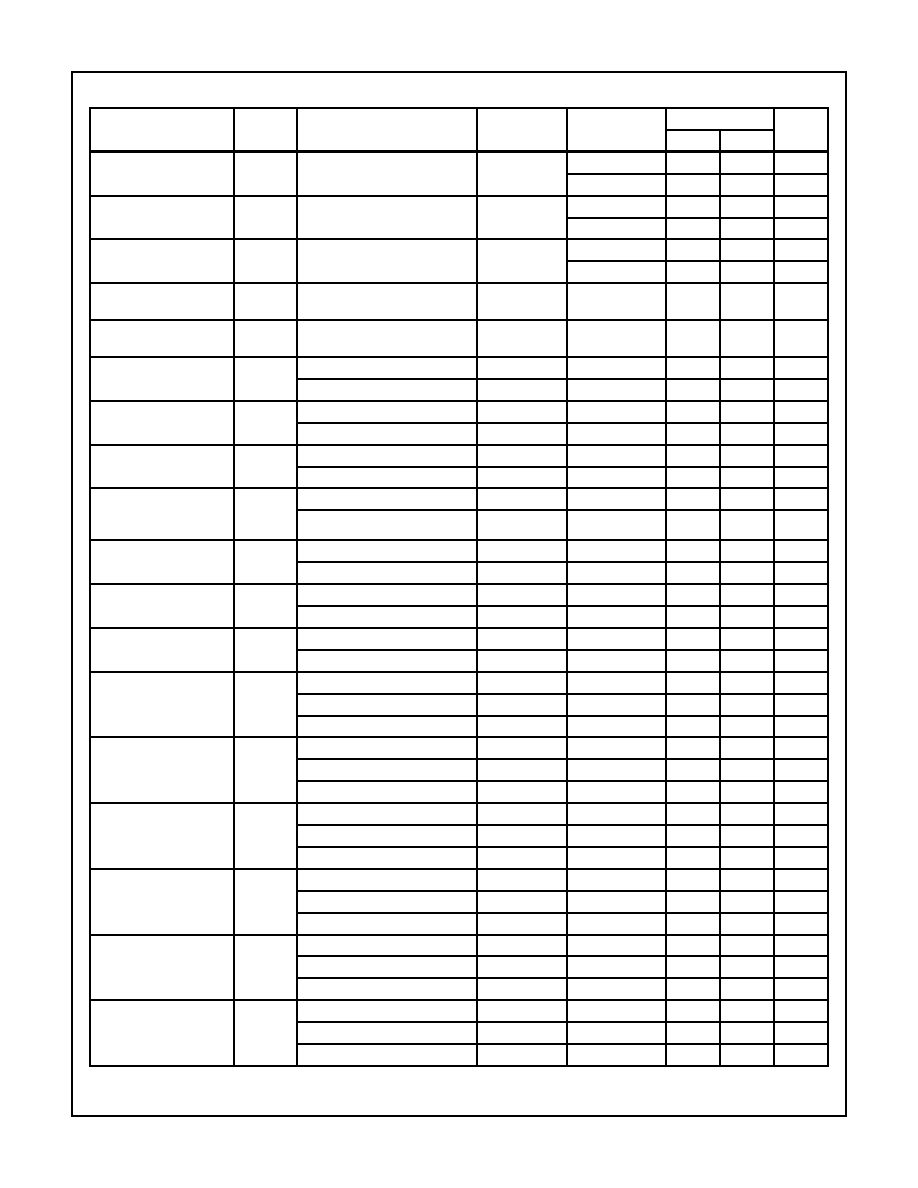
TABLE 2. AC ELECTRICAL PERFORMANCE CHARACTERISTICS
PARAMETER
SYMBOL
CONDITIONS (NOTE 1, 2)
GROUP A
SUBGROUPS
TEMPERATURE
LIMITS
UNITS
MIN
MAX
Propagation Delay
Clock To Q Output
TPHL1
TPLH1
VDD = 5V, VIN = VDD or GND
9
+25
o
C
-
500
ns
10, 11
+125
o
C, -55
o
C
-
675
ns
Propagation Delay
Clock To Carry Out
TPHL2
TPLH2
VDD = 5V, VIN = VDD or GND
9
+25
o
C
-
560
ns
10, 11
+125
o
C, -55
o
C
-
756
ns
Propagation Delay
Preset Enable To Q
TPHL3
TPLH3
VDD = 5V, VIN = VDD or GND
9
+25
o
C
-
470
ns
10, 11
+125
o
C, -55
o
C
-
635
ns
Propagation Delay
Preset Enable To Carry-
Out
TPHL4
TPLH4
VDD = 5V, VIN = VDD or GND
9
+25
o
C
-
640
ns
10, 11
+125
o
C, -55
o
C
-
864
ns
Propagation Delay
Carry-In To
Carry-Out
TPHL5
TPLH5
VDD = 5V, VIN = VDD or GND
9
+25
o
C
-
340
ns
10, 11
+125
o
C, -55
o
C
-
459
ns
Transition Time
Q Output
TTHL
TTLH
VDD = 5V, VIN = VDD or GND
9
+25
o
C
-
200
ns
10, 11
+125
o
C, -55
o
C
-
270
ns
Maximum Clock Input
Frequency
FCL
VDD = 5V, VIN = VDD or GND
9
+25
o
C
2
-
MHz
10, 11
+125
o
C, -55
o
C
1.48
-
MHz
NOTES:
1. VDD = 5V, CL = 50pF, RL = 200K
2. -55
o
C and +125
o
C limits guaranteed, 100% testing being implemented.
TABLE 3. ELECTRICAL PERFORMANCE CHARACTERISTICS
PARAMETER
SYMBOL
CONDITIONS
NOTES
TEMPERATURE
LIMITS
UNITS
MIN
MAX
Supply Current
IDD
VDD = 5V, VIN = VDD or GND
1, 2
-55
o
C, +25
o
C
-
5
µ
A
+125
o
C
-
150
µ
A
VDD = 10V, VIN = VDD or GND
1, 2
-55
o
C, +25
o
C
-
10
µ
A
+125
o
C
-
300
µ
A
VDD = 15V, VIN = VDD or GND
1, 2
-55
o
C, +25
o
C
-
10
µ
A
+125
o
C
-
600
µ
A
Output Voltage
VOL
VDD = 5V, No Load
1, 2
+25
o
C, +125
o
C,
-55
o
C
-
50
mV
Output Voltage
VOL
VDD = 10V, No Load
1, 2
+25
o
C, +125
o
C,
-55
o
C
-
50
mV
Output Voltage
VOH
VDD = 5V, No Load
1, 2
+25
o
C, +125
o
C,
-55
o
C
4.95
-
V
Output Voltage
VOH
VDD = 10V, No Load
1, 2
+25
o
C, +125
o
C,
-55
o
C
9.95
-
V
Output Current (Sink)
IOL5
VDD = 5V, VOUT = 0.4V
1, 2
+125
o
C
0.36
-
mA
-55
o
C
0.64
-
mA
Output Current (Sink)
IOL10
VDD = 10V, VOUT = 0.5V
1, 2
+125
o
C
0.9
-
mA
-55
o
C
1.6
-
mA
Output Current (Sink)
IOL15
VDD = 15V, VOUT = 1.5V
1, 2
+125
o
C
2.4
-
mA
-55
o
C
4.2
-
mA
Output Current (Source)
IOH5A
VDD = 5V, VOUT = 4.6V
1, 2
+125
o
C
-
-0.36
mA
-55
o
C
-
-0.64
mA
7-801
Specifications CD4029BMS
Output Current (Source)
IOH5B
VDD = 5V, VOUT = 2.5V
1, 2
+125
o
C
-
-1.15
mA
-55
o
C
-
-2.0
mA
Output Current (Source)
IOH10
VDD = 10V, VOUT = 9.5V
1, 2
+125
o
C
-
-0.9
mA
-55
o
C
-
-2.6
mA
Output Current (Source)
IOH15
VDD =15V, VOUT = 13.5V
1, 2
+125
o
C
-
-2.4
mA
-55
o
C
-
-4.2
mA
Input Voltage Low
VIL
VDD = 10V, VOH > 9V, VOL < 1V
1, 2
+25
o
C, +125
o
C,
-55
o
C
-
3
V
Input Voltage High
VIH
VDD = 10V, VOH > 9V, VOL < 1V
1, 2
+25
o
C, +125
o
C,
-55
o
C
7
-
V
Propagation Delay
Q Output
TPHL1
TPLH1
VDD = 10V
1, 2, 3
+25
o
C
-
240
ns
VDD = 15V
1, 2, 3
+25
o
C
-
180
ns
Propagation Delay
Carry Output
TPHL2
TPLH2
VDD = 10V
1, 2, 3
+25
o
C
-
260
ns
VDD = 15V
1, 2, 3
+25
o
C
-
190
ns
Propagation Delay
Preset Enable To Q
TPHL3
TPLH3
VDD = 10V
1, 2, 3
+25
o
C
-
200
ns
VDD = 15V
1, 2, 3
+25
o
C
-
160
ns
Propagation Delay
Preset Enable To Carry-
Out
TPHL4
TPLH4
VDD = 10V
1, 2, 3
+25
o
C
-
290
ns
VDD = 15V
1, 2, 3
+25
o
C
-
210
ns
Propagation Delay
Carry In To Carry Out
TPHL5
TPLH5
VDD = 10V
1, 2, 3
+25
o
C
-
140
ns
VDD = 15V
1, 2, 3
+25
o
C
-
100
ns
Transition Time
TTHL
TTLH
VDD = 10V
1, 2, 3
+25
o
C
-
100
ns
VDD = 15V
1, 2, 3
+25
o
C
-
80
ns
Maximum Clock Input
Frequency
FCL
VDD = 10V
1, 2, 3
+25
o
C
4
-
MHz
VDD = 15V
1, 2, 3
+25
o
C
5.5
-
MHz
Minimum Data Setup
Time
Note 4
TS
VDD = 5V
1, 2, 3
+25
o
C
-
340
ns
VDD = 10V
1, 2, 3
+25
o
C
-
140
ns
VDD = 15V
1, 2, 3
+25
o
C
-
100
ns
Clock Rise And Fall Time
Note 5
TRCL
TFCL
VDD = 5V
1, 2, 3
+25
o
C
-
15
µ
s
VDD = 10V
1, 2, 3
+25
o
C
-
15
µ
s
VDD = 15V
1, 2, 3
+25
o
C
-
15
µ
s
Minimum Clock Pulse
Width
TW
VDD = 5V
1, 2, 3
+25
o
C
-
180
ns
VDD = 10V
1, 2, 3
+25
o
C
-
90
ns
VDD = 15V
1, 2, 3
+25
o
C
-
60
ns
Minimum Carry In Setup
Time
Note 6
TS
VDD = 5V
1, 2, 3
+25
o
C
-
200
ns
VDD = 10V
1, 2, 3
+25
o
C
-
70
ns
VDD = 15V
1, 2, 3
+25
o
C
-
60
ns
Minimum Carry Input
Hold Time
Note 6
TH
VDD = 5V
1, 2, 3
+25
o
C
-
50
ns
VDD = 10V
1, 2, 3
+25
o
C
-
30
ns
VDD = 15V
1, 2, 3
+25
o
C
-
25
ns
Minimum Preset Enable
Removal Time
Note 4
TREM
VDD = 5V
1, 2, 3
+25
o
C
-
200
ns
VDD = 10V
1, 2, 3
+25
o
C
-
110
ns
VDD = 15V
1, 2, 3
+25
o
C
-
80
ns
TABLE 3. ELECTRICAL PERFORMANCE CHARACTERISTICS
(Continued)
PARAMETER
SYMBOL
CONDITIONS
NOTES
TEMPERATURE
LIMITS
UNITS
MIN
MAX
7-802
Specifications CD4029BMS
Minimum Preset Enable
Pulse Width
TW
VDD = 5V
1, 2, 3
+25
o
C
-
130
ns
VDD = 10V
1, 2, 3
+25
o
C
-
70
ns
VDD = 15V
1, 2, 3
+25
o
C
-
50
ns
Input Capacitance
CIN
Any Input
1, 2
+25
o
C
-
7.5
pF
NOTES:
1. All voltages referenced to device GND.
2. The parameters listed on Table 3 are controlled via design or process and are not directly tested. These parameters are characterized
on initial design release and upon design changes which would affect these characteristics.
3. CL = 50pF, RL = 200K, Input TR, TF < 20ns.
4. From Up/Down, Binary/Decode, Carry In, or Preset Enable Control Inputs to Clock Edge.
5. If more than one unit is cascaded in the parallel clocked application, tr CL should be made
the sum of the fixed propagation delay at
15pF and the transition time of the carry output driving stage for the estimated capacitive load. This measurement was made with a de-
coupling capacitor (>1
µ
F) between VDD and VSS.
6. From Carry In to Clock Edge.
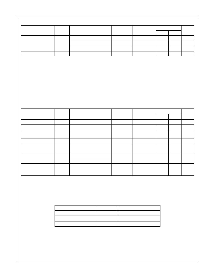
TABLE 4. POST IRRADIATION ELECTRICAL PERFORMANCE CHARACTERISTICS
PARAMETER
SYMBOL
CONDITIONS
NOTES
TEMPERATURE
LIMITS
UNITS
MIN
MAX
Supply Current
IDD
VDD = 20V, VIN = VDD or GND
1, 4
+25
o
C
-
25
µ
A
N Threshold Voltage
VNTH
VDD = 10V, ISS = -10
µ
A
1, 4
+25
o
C
-2.8
-0.2
V
N Threshold Voltage
Delta
VTN
VDD = 10V, ISS = -10
µ
A
1, 4
+25
o
C
-
±
1
V
P Threshold Voltage
VTP
VSS = 0V, IDD = 10
µ
A
1, 4
+25
o
C
0.2
2.8
V
P Threshold Voltage
Delta
VTP
VSS = 0V, IDD = 10
µ
A
1, 4
+25
o
C
-
±
1
V
Functional
F
VDD = 18V, VIN = VDD or GND
1
+25
o
C
VOH >
VDD/2
VOL <
VDD/2
V
VDD = 3V, VIN = VDD or GND
Propagation Delay Time
TPHL
TPLH
VDD = 5V
1, 2, 3, 4
+25
o
C
-
1.35 x
+25
o
C
Limit
ns
NOTES: 1. All voltages referenced to device GND.
2. CL = 50pF, RL = 200K, Input TR, TF < 20ns
3. See Table 2 for +25
o
C limit.
4. Read and Record
TABLE 5. BURN-IN AND LIFE TEST DELTA PARAMETERS +25
O
C
PARAMETER
SYMBOL
DELTA LIMIT
Supply Current - MSI-2
IDD
±
1.0
µ
A
Output Current (Sink)
IOL5
±
20% x Pre-Test Reading
Output Current (Source)
IOH5A
±
20% x Pre-Test Reading
TABLE 3. ELECTRICAL PERFORMANCE CHARACTERISTICS
(Continued)
PARAMETER
SYMBOL
CONDITIONS
NOTES
TEMPERATURE
LIMITS
UNITS
MIN
MAX