 | –≠–ª–µ–∫—Ç—Ä–æ–Ω–Ω—ã–π –∫–æ–º–ø–æ–Ω–µ–Ω—Ç: CD4031BMS | –°–∫–∞—á–∞—Ç—å:  PDF PDF  ZIP ZIP |
7-816
CAUTION: These devices are sensitive to electrostatic discharge; follow proper IC Handling Procedures.
1-888-INTERSIL or 321-724-7143 | Copyright © Intersil Corporation 1999
CD4031BMS
CMOS 64-Stage Static Shift Register
Description
The CD4031BMS is a static shift register that contains 64 D-
type, master-slave flip-flop stages and one stage which is a
D-type master flip-flop only (referred to as a 1/2 stage).
The logic level present at the DATA input is transferred into
the first stage and shifted one stage at each positive-going
clock transition. Maximum clock frequencies up to 12MHz
(typical) can be obtained. Because fully static operation is
allowed, information can be permanently stored with the
clock line in either the low or high state. The CD4031BMS
has a MODE CONTROL input that, when in the high state,
allows operation in the recirculating mode. The MODE CON-
TROL input can also be used to select between two sepa-
rate data sources. Register packages can be cascaded and
the clock lines driven directly for high-speed operation. Alter-
natively, a delayed clock output (CLD) is provided that
enables cascading register packages while allowing reduced
clock drive fan-out and transition-time requirements. A third
cascading option makes use of the Q' output from the 1/2
stage, which is available on the next negative-going transi-
tion of the clock after the Q output occurs. This delayed out-
put, like the delayed clock CLD, is used with clocks having
slow rise and fall times.
The CD4031BMS is supplied in these 16 lead outline pack-
ages:
Braze Seal DIP
H4X
Frit Seal DIP
H1F
Ceramic Flatpack
H6W
Features
∑ High Voltage Type (20V Rating)
∑ Fully Static Operation: DC to 12MHz (typ.) at VDD -
VSS = 15V
∑ Standard TTL Drive Capability on Q Output
∑ Recirculation Capability
∑ Three Cascading Modes:
- Direct Clocking for High-Speed Operation
- Delayed Clocking for Reduced Clock Drive Require-
ments
- Additional 1/2 Stage for Slow Clocks
∑ 100% Tested For Quiescent Current at 20V
∑ Maximum Input Current of 1
µ
A at 18V Over Full
Package-Temperature Range;
- 100nA at 18V and +25
o
C
∑ Noise Margin (Over Full Package Temperature Range):
- 1V at VDD = 5V
- 2V at VDD = 10V
- 2.5V at VDD = 15V
∑ 5V, 10V and 15V Parametric Ratings
∑ Meets All Requirements of JEDEC Tentative Standard
No. 13B, "Standard Specifications for Description of
`B' Series CMOS Devices"
Applications
∑ Serial Shift Registers
∑ Time Delay Circuits
December 1992
File Number
3306
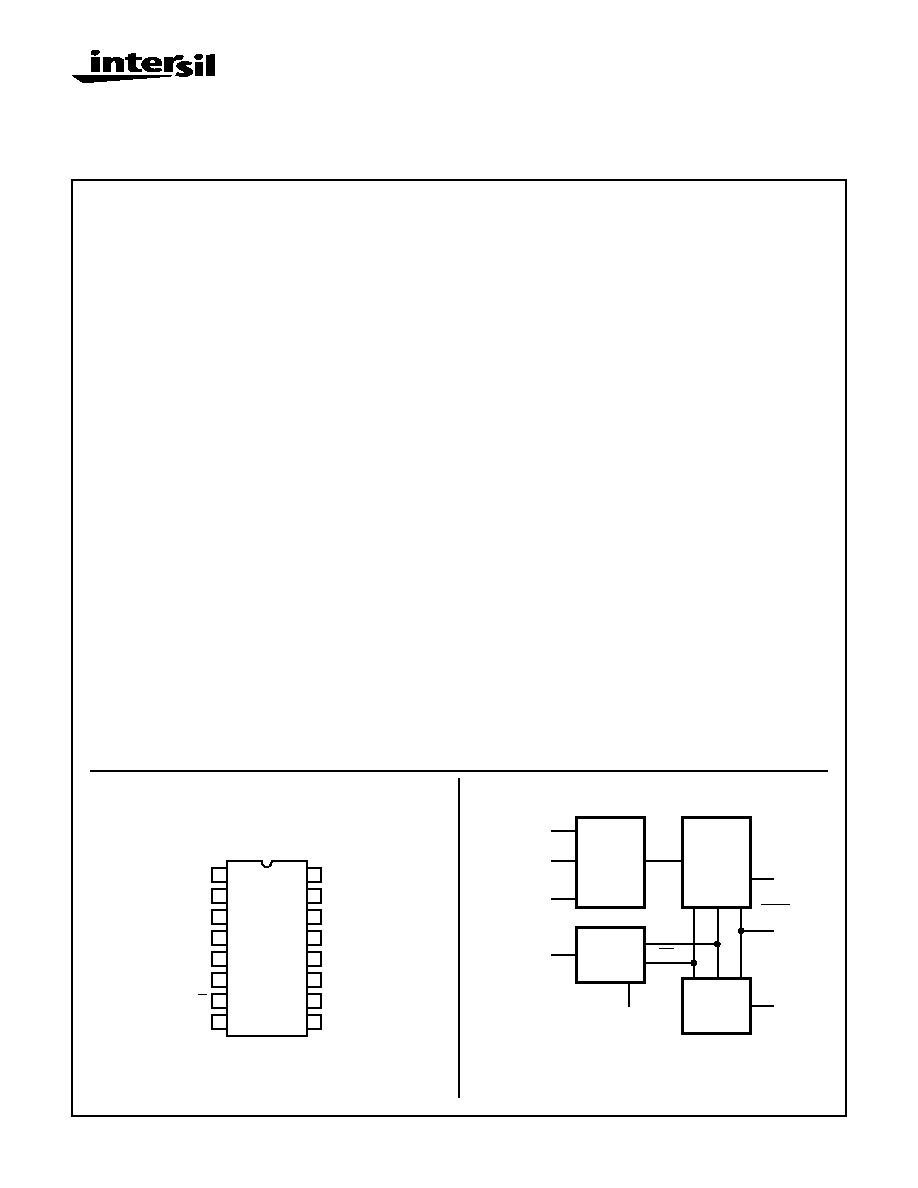
Pinout
CD4031BMS
TOP VIEW
14
15
16
9
13
12
11
10
1
2
3
4
5
7
6
8
DATA IN 2
CLOCK INHIBIT
NC
NC
Q'
Q
VSS
Q
VDD
NC
NC
NC
NC
MODE CONTROL
CLD
DATA IN 1
RECIRCULATE
NC = NO CONNECTION
Functional Diagram
CONTROL
LOGIC
64
STAGES
CLOCK
LOGIC
1/2
STAGE
DATA 1
IN
MODE
CONT.
RECIRC
DATA 2
IN
CLOCK
IN
VDD = 16
VSS = 8
NC = 3, 4, 11, 12, 13, 14
DELAYED
CLOCK
OUT
DATA
OUT
6
DATA
OUT
7
Q'
5
15
10
1
2
9
CL
CL
7-817
Specifications CD4031BMS
Absolute Maximum Ratings
Reliability Information
DC Supply Voltage Range, (VDD) . . . . . . . . . . . . . . . -0.5V to +20V
(Voltage Referenced to VSS Terminals)
Input Voltage Range, All Inputs . . . . . . . . . . . . .-0.5V to VDD +0.5V
DC Input Current, Any One Input
. . . . . . . . . . . . . . . . . . . . . . . .±
10mA
Operating Temperature Range . . . . . . . . . . . . . . . . -55
o
C to +125
o
C
Package Types D, F, K, H
Storage Temperature Range (TSTG) . . . . . . . . . . . -65
o
C to +150
o
C
Lead Temperature (During Soldering) . . . . . . . . . . . . . . . . . +265
o
C
At Distance 1/16
±
1/32 Inch (1.59mm
±
0.79mm) from case for
10s Maximum
Thermal Resistance . . . . . . . . . . . . . . . .
ja
jc
Ceramic DIP and FRIT Package . . . . .
80
o
C/W
20
o
C/W
Flatpack Package . . . . . . . . . . . . . . . .
70
o
C/W
20
o
C/W
Maximum Package Power Dissipation (PD) at +125
o
C
For TA = -55
o
C to +100
o
C (Package Type D, F, K) . . . . . . 500mW
For TA = +100
o
C to +125
o
C (Package Type D, F, K) . . . . . Derate
Linearity at 12mW/
o
C to 200mW
Device Dissipation per Output Transistor . . . . . . . . . . . . . . . 100mW
For TA = Full Package Temperature Range (All Package Types)
Junction Temperature . . . . . . . . . . . . . . . . . . . . . . . . . . . . . . +175
o
C
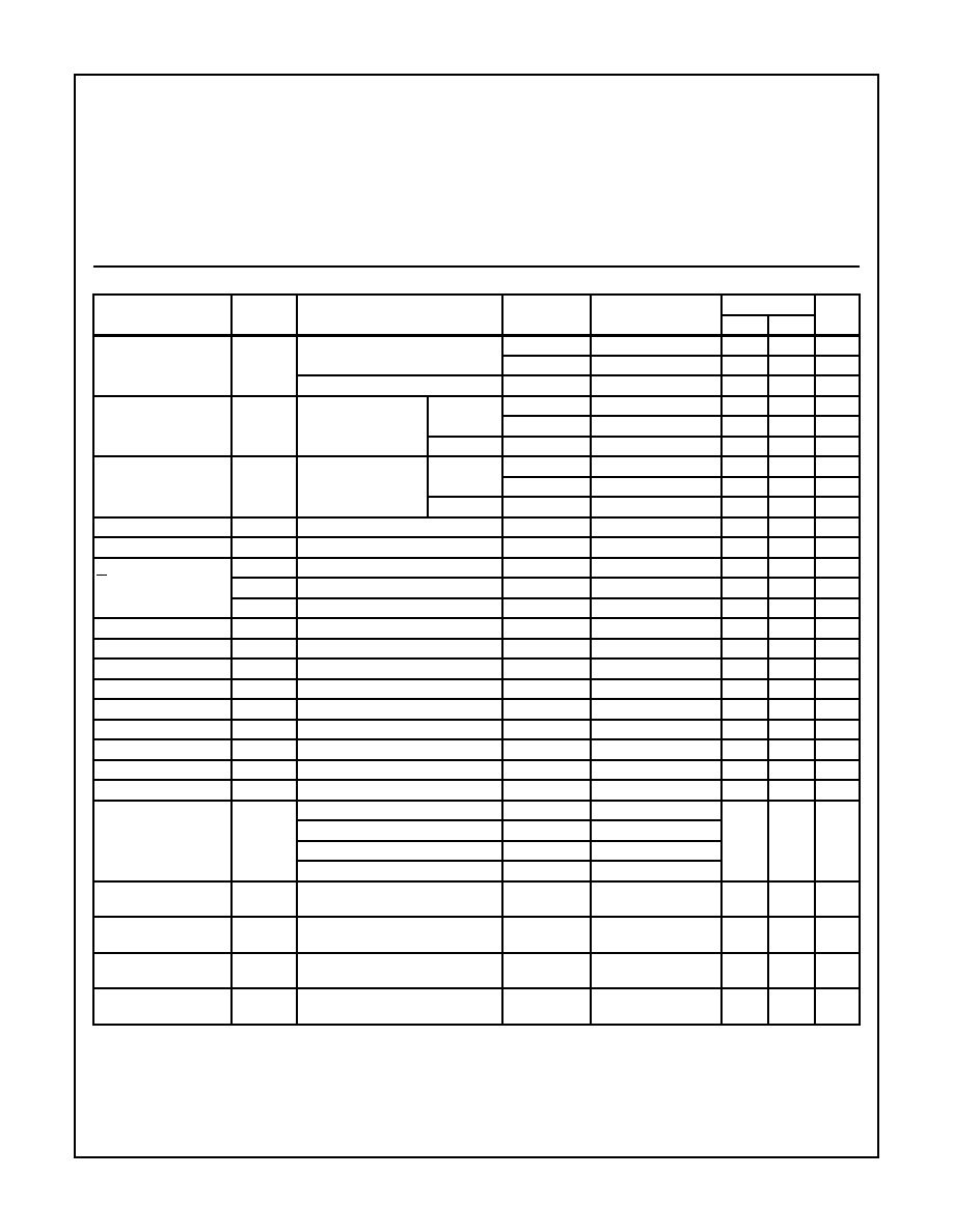
TABLE 1. DC ELECTRICAL PERFORMANCE CHARACTERISTICS
PARAMETER
SYMBOL
CONDITIONS (NOTE 1)
GROUP A
SUBGROUPS
TEMPERATURE
LIMITS
UNITS
MIN
MAX
Supply Current
IDD
VDD = 20V, VIN = VDD or GND
1
+25
o
C
-
10
µ
A
2
+125
o
C
-
1000
µ
A
VDD = 18V, VIN = VDD or GND
3
-55
o
C
-
10
µ
A
Input Leakage Current
IIL
VIN = VDD or GND
VDD = 20
1
+25
o
C
-100
-
nA
2
+125
o
C
-1000
-
nA
VDD = 18V
3
-55
o
C
-100
-
nA
Input Leakage Current
IIH
VIN = VDD or GND
VDD = 20
1
+25
o
C
-
100
nA
2
+125
o
C
-
1000
nA
VDD = 18V
3
-55
o
C
-
100
nA
Output Voltage
VOL15
VDD = 15V, No Load
1, 2, 3
+25
o
C, +125
o
C, -55
o
C
-
50
mV
Output Voltage
VOH15
VDD = 15V, No Load (Note 3)
1, 2, 3
+25
o
C, +125
o
C, -55
o
C 14.95
-
V
Output Current
Q, Q', CLD
IOL5
VDD = 5V, VOUT = 0.4V
1
+25
o
C
0.51
-
mA
IOL10
VDD = 10V, VOUT = 0.5V
1
+25
o
C
1.3
-
mA
IOL15
VDD = 15V, VOUT = 1.5V
1
+25
o
C
3.4
-
mA
Output Current Q
IOL5
VDD = 5V, VOUT = 0.4V
1
+25
o
C
2.04
-
mA
Output Current Q
IOL10
VDD = 10V, VOUT = 0.5V
1
+25
o
C
5.2
-
mA
Output Current Q
IOL15
VDD = 15V, VOUT = 1.5V
1
+25
o
C
13.6
-
mA
Output Current (Source)
IOH5A
VDD = 5V, VOUT = 4.6V
1
+25
o
C
-
-0.51
mA
Output Current (Source)
IOH5B
VDD = 5V, VOUT = 2.5V
1
+25
o
C
-
-1.6
mA
Output Current (Source)
IOH10
VDD = 10V, VOUT = 9.5V
1
+25
o
C
-
-1.3
mA
Output Current (Source)
IOH15
VDD = 15V, VOUT = 13.5V
1
+25
o
C
-
-3.4
mA
N Threshold Voltage
VNTH
VDD = 10V, ISS = -10
µ
A
1
+25
o
C
-2.8
-0.7
V
P Threshold Voltage
VPTH
VSS = 0V, IDD = 10
µ
A
1
+25
o
C
0.7
2.8
V
Functional
F
VDD = 2.8V, VIN = VDD or GND
7
+25
o
C
VOH >
VDD/2
VOL <
VDD/2
V
VDD = 20V, VIN = VDD or GND
7
+25
o
C
VDD = 18V, VIN = VDD or GND
8A
+125
o
C
VDD = 3V, VIN = VDD or GND
8B
-55
o
C
Input Voltage Low
(Note 2)
VIL
VDD = 5V, VOH > 4.5V, VOL < 0.5V
1, 2, 3
+25
o
C, +125
o
C, -55
o
C
-
1.5
V
Input Voltage High
(Note 2)
VIH
VDD = 5V, VOH > 4.5V, VOL < 0.5V
1, 2, 3
+25
o
C, +125
o
C, -55
o
C
3.5
-
V
Input Voltage Low
(Note 2)
VIL
VDD = 15V, VOH > 13.5V,
VOL < 1.5V
1, 2, 3
+25
o
C, +125
o
C, -55
o
C
-
4
V
Input Voltage High
(Note 2)
VIH
VDD = 15V, VOH > 13.5V,
VOL < 1.5V
1, 2, 3
+25
o
C, +125
o
C, -55
o
C
11
-
V
NOTES: 1. All voltages referenced to device GND, 100% testing being
implemented.
2. Go/No Go test with limits applied to inputs.
3. For accuracy, voltage is measured differentially to VDD. Limit
is 0.050V max.
7-818
Specifications CD4031BMS
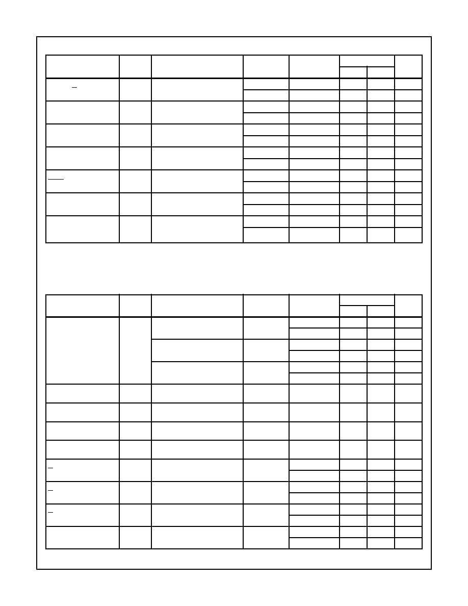
TABLE 2. AC ELECTRICAL PERFORMANCE CHARACTERISTICS
PARAMETER
SYMBOL
CONDITIONS (NOTE 1, 2)
GROUP A
SUBGROUPS
TEMPERATURE
LIMITS
UNITS
MIN
MAX
Propagation Delay
Clock to Q
TPHL1
TPLH1
VDD = 5V, VIN = VDD or GND
9
+25
o
C
-
500
ns
10, 11
+125
o
C, -55
o
C
-
675
ns
Propagation Delay
Clock to Q
TPLH2
VDD = 5V, VIN = VDD or GND
9
+25
o
C
-
500
ns
10, 11
+125
o
C, -55
o
C
-
675
ns
Propagation Delay
Clock to Q
TPHL2
VDD = 5V, VIN = VDD or GND
9
+25
o
C
-
380
ns
10, 11
+125
o
C, -55
o
C
-
513
ns
Propagation Delay
Clock to Q'
TPLH3
TPHL3
VDD = 5V, VIN = VDD or GND
9
+25
o
C
-
380
ns
10, 11
+125
o
C, -55
o
C
-
513
ns
Propagation Delay
Clock to CLD
TPHL4
TPLH4
VDD = 5V, VIN = VDD or GND
9
+25
o
C
-
200
ns
10, 11
+125
o
C, -55
o
C
-
270
ns
Transition Time
TTHL
TTLH
VDD = 5V, VIN = VDD or GND
9
+25
o
C
-
200
ns
10, 11
+125
o
C, -55
o
C
-
270
ns
Maximum Clock Input
Frequency (See Note 5;
Table 3)
FCL
VDD = 5V, VIN = VDD or GND
9
+25
o
C
2
-
MHz
10, 11
+125
o
C, -55
o
C
1.48
-
MHz
NOTES:
1. CL = 50pF, RL = 200K, Input TR, TF < 20ns.
2. -55
o
C and +125
o
C limits guaranteed, 100% testing being implemented.
TABLE 3. ELECTRICAL PERFORMANCE CHARACTERISTICS
PARAMETER
SYMBOL
CONDITIONS
NOTES
TEMPERATURE
LIMITS
UNITS
MIN
MAX
Supply Current
IDD
VDD = 5V, VIN = VDD or GND
1, 2
-55
o
C, +25
o
C
-
5
µ
A
+125
o
C
-
150
µ
A
VDD = 10V, VIN = VDD or GND
1, 2
-55
o
C, +25
o
C
-
10
µ
A
+125
o
C
-
300
µ
A
VDD = 15V, VIN = VDD or GND
1, 2
-55
o
C, +25
o
C
-
10
µ
A
+125
o
C
-
600
µ
A
Output Voltage
VOL
VDD = 5V, No Load
1, 2
+25
o
C, +125
o
C,
-55
o
C
-
50
mV
Output Voltage
VOL
VDD = 10V, No Load
1, 2
+25
o
C, +125
o
C,
-55
o
C
-
50
mV
Output Voltage
VOH
VDD = 5V, No Load
1, 2
+25
o
C, +125
o
C,
-55
o
C
4.95
-
V
Output Voltage
VOH
VDD = 10V, No Load
1, 2
+25
o
C, +125
o
C,
-55
o
C
9.95
-
V
Output Current (Sink)
Q, Q', CLD Outputs
IOL5
VDD = 5V, VOUT = 0.4V
1, 2
+125
o
C
0.36
-
mA
-55
o
C
0.64
-
mA
Output Current (Sink)
Q, Q', CLD Outputs
IOL10
VDD = 10V, VOUT = 0.5V
1, 2
+125
o
C
0.9
-
mA
-55
o
C
1.6
-
mA
Output Current (Sink)
Q, Q', CLD Outputs
IOL15
VDD = 15V, VOUT = 1.5V
1, 2
+125
o
C
2.4
-
mA
-55
o
C
4.2
-
mA
Output Current (Sink)
Q Outputs
IOL5
VDD = 5V, VOUT = 0.4V
1, 2
+125
o
C
1.44
-
mA
-55
o
C
2.56
-
mA

7-819
Specifications CD4031BMS
Output Current (Sink)
Q Outputs
IOL10
VDD = 10V, VOUT = 0.5V
1, 2
+125
o
C
3.6
-
mA
-55
o
C
6.4
-
mA
Output Current (Sink)
Q Outputs
IOL15
VDD = 15V, VOUT = 1.5V
1, 2
+125
o
C
9.6
-
mA
-55
o
C
16.8
-
mA
Output Current (Source)
IOH5A
VDD = 5V, VOUT = 4.6V
1, 2
+125
o
C
-
-0.36
mA
-55
o
C
-
-0.64
mA
Output Current (Source)
IOH5B
VDD = 5V, VOUT = 2.5V
1, 2
+125
o
C
-
-1.15
mA
-55
o
C
-
-2.0
mA
Output Current (Source)
IOH10
VDD = 10V, VOUT = 9.5V
1, 2
+125
o
C
-
-0.9
mA
-55
o
C
-
-1.6
mA
Output Current (Source)
IOH15
VDD =15V, VOUT = 13.5V
1, 2
+125
o
C
-
-2.4
mA
-55
o
C
-
-4.2
mA
Input Voltage Low
VIL
VDD = 10V, VOH > 9V, VOL < 1V
1, 2
+25
o
C, +125
o
C,
-55
o
C
-
3
V
Input Voltage High
VIH
VDD = 10V, VOH > 9V, VOL < 1V
1, 2
+25
o
C, +125
o
C,
-55
o
C
+7
-
V
Propagation Delay
Clock to Q
TPHL1
TPLH1
VDD = 10V
1, 2, 3
+25
o
C
-
220
ns
VDD = 15V
1, 2, 3
+25
o
C
-
180
ns
Propagation Delay
Clock to Q
TPLH2
VDD = 10V
1, 2, 3
+25
o
C
-
220
ns
VDD = 15V
1, 2, 3
+25
o
C
-
180
ns
Propagation Delay
Clock to Q
TPHL2
VDD = 10V
1, 2, 3
+25
o
C
-
160
ns
VDD = 15V
1, 2, 3
+25
o
C
-
130
ns
Propagation Delay
Clock to CLD
TPLH3
TPHL3
VDD = 10V
1, 2, 3
+25
o
C
-
100
ns
VDD = 15V
1, 2, 3
+25
o
C
-
80
ns
Propagation Delay
Clock to Q'
TPLH4
TPHL4
VDD = 10V
1, 2, 3
+25
o
C
-
160
ns
VDD = 15V
1, 2, 3
+25
o
C
-
130
ns
Transition Time
TTHL
TTLH
VDD = 10V
1, 2, 3
+25
o
C
-
100
ns
VDD = 15V
1, 2, 3
+25
o
C
-
80
ns
Maximum Clock Input
Frequency (Note 5)
FCL
VDD = 10V
1, 2, 3
+25
o
C
-
5
MHz
VDD = 15V
1, 2, 3
+25
o
C
-
6
MHz
Clock Input Rise or Fall
Time (Note 4)
TRCL
TFCL
VDD = 5V
1, 2, 3
+25
o
C
-
1000
µ
s
VDD = 10V
1, 2, 3
+25
o
C
-
1000
µ
s
VDD = 15V
1, 2, 3
+25
o
C
-
200
µ
s
Minimum Data Setup
Time
TS
VDD = 5V
1, 2, 3
+25
o
C
-
60
ns
VDD = 10V
1, 2, 3
+25
o
C
-
30
ns
VDD = 15V
1, 2, 3
+25
o
C
-
20
ns
Minimum Data Hold Time
TH
VDD = 5V
1, 2, 3
+25
o
C
-
60
ns
VDD = 10V
1, 2, 3
+25
o
C
-
30
ns
VDD = 15V
1, 2, 3
+25
o
C
-
20
ns
Minimum Clock Pulse
Width
TW
VDD = 5V
1, 2, 3
+25
o
C
-
240
ns
VDD = 10V
1, 2, 3
+25
o
C
-
100
ns
VDD = 15V
1, 2, 3
+25
o
C
-
80
ns
Input Capacitance
CIN
Any Input
1, 2
+25
o
C
-
7.5
pF
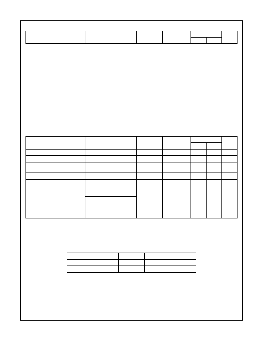
TABLE 3. ELECTRICAL PERFORMANCE CHARACTERISTICS
(Continued)
PARAMETER
SYMBOL
CONDITIONS
NOTES
TEMPERATURE
LIMITS
UNITS
MIN
MAX
7-820
Specifications CD4031BMS
NOTES:
1. All voltages referenced to device GND.
2. The parameters listed on Table 3 are controlled via design or process and are not directly tested. These parameters are characterized
on initial design release and upon design changes which would affect these characteristics.
3. CL = 50pF, RL = 200K, Input TR, TF < 20ns.
4. If more than one unit is cascaded in the parallel clocked application, TRCL should be made
the sum of the propagation delay at 50pF
and the transition time of the output driving stage.
5. Maximum clock frequency for cascaded units;
a) Using Delayed Clock feature in recirculation mode:
b) Not using Delayed Clock:
TABLE 4. POST IRRADIATION ELECTRICAL PERFORMANCE CHARACTERISTICS
PARAMETER
SYMBOL
CONDITIONS
NOTES
TEMPERATURE
LIMITS
UNITS
MIN
MAX
Supply Current
IDD
VDD = 20V, VIN = VDD or GND
1, 4
+25
o
C
-
25
µ
A
N Threshold Voltage
VNTH
VDD = 10V, ISS = -10
µ
A
1, 4
+25
o
C
-2.8
-0.2
V
N Threshold Voltage
Delta
VNTH
VDD = 10V, ISS = -10
µ
A
1, 4
+25
o
C
-
±
1
V
P Threshold Voltage
VPTH
VSS = 0V, IDD = 10
µ
A
1, 4
+25
o
C
0.2
2.8
V
P Threshold Voltage
Delta
VPTH
VSS = 0V, IDD = 10
µ
A
1, 4
+25
o
C
-
±
1
V
Functional
F
VDD = 18V, VIN = VDD or GND
1
+25
o
C
VOH >
VDD/2
VOL <
VDD/2
V
VDD = 3V, VIN = VDD or GND
Propagation Delay Time
TPHL
TPLH
VDD = 5V (Worst Case)
1, 2, 3, 4
+25
o
C
-
1.35 x
+25
o
C
Limit
ns
NOTES:
1. All voltages referenced to device GND.
2. VDD = 5V, CL = 50pF, RL = 200K
3. See Table 2 for +25
o
C limit.
TABLE 5. BURN-IN AND LIFE TEST DELTA PARAMETERS +25
O
C
PARAMETER
SYMBOL
DELTA LIMIT
Supply Current - MSI-2
IDD
±
1.0
µ
A
Output Current (Sink)
IOL5
±
20% x Pre-Test Reading
TABLE 3. ELECTRICAL PERFORMANCE CHARACTERISTICS
(Continued)
PARAMETER
SYMBOL
CONDITIONS
NOTES
TEMPERATURE
LIMITS
UNITS
MIN
MAX
FMAX
1
n-1
(
)
CL, prop delay and Q prop delay and set
up time
≠
--------------------------------------------------------------------------------------------------------------------------------------
where n
number of packages
=
=
FMAX
1
propagation delay and set
up time
≠
----------------------------------------------------------------------------
=