
1
TM
Features
∑ Instruction Time of 3.2
µ
s, -40
o
C to +85
o
C
∑ 123 Instructions - Upwards Software Compatible With
CDP1802
∑ BCD Arithmetic Instructions
∑ Low-Power IDLE Mode
∑ Pin Compatible With CDP1802 Except for Terminal 16
∑ 64K-Byte Memory Address Capability
∑ 64 Bytes of On-Chip RAM
∑ 16 x 16 Matrix of On-Board Registers
∑ On-Chip Crystal or RC Controlled Oscillator
∑ 8-Bit Counter/Timer
Description
The CDP1805AC and CDP1806AC are functional and per-
formance enhancements of the CDP1802 CMOS 8-bit regis-
ter-oriented microprocessor series and are designed for use
in general-purpose applications.
The CDP1805AC hardware enhancements include a 64-
byte RAM and an 8-bit presettable down counter. The
Counter/Timer which generates an internal interrupt request,
can be programmed for use in timebase, event-counting,
and pulse-duration measurement applications. The
Counter/Timer underflow output can also be directed to the
Q output terminal. The CDP1806AC hardware enhance-
ments are identical to the CDP1805AC, except the
CDP1806AC contains no on-chip RAM.
The CDP1805AC and CDP1806AC software enhancements
include 32 more instructions than the CDP1802. The 32 new
software instructions add subroutine call and return capabil-
ity, enhanced data transfer manipulation, Counter/Timer con-
trol, improved interrupt handling, single-instruction loop
counting, and BCD arithmetic.
Upwards software and hardware compatibility is maintained
when substituting a CDP1805AC or CDP1806AC for other
CDP1800-series microprocessors. Pinout is identical except
for the replacement of V
CC
with ME on the CDP1805AC and
the replacement of V
CC
with V
DD
on the CDP1806AC.
n
CDP1805AC Only
Ordering Information
CDP1805AC
CDP1806AC
TEMPERATURE RANGE
PACKAGE
PKG. NO.
CDP1805ACE
CDP1806ACE
-40
o
C to +85
o
C
Plastic DIP
E40.6
-
CDP1806ACEX
Burn-In
CDP1805ACQ
CDP1806ACQ
-40
o
C to +85
o
C
PLCC
N44.65
CDP1805ACD
CDP1806ACD
-40
o
C to +85
o
C
SBDIP
D40.6
CDP1805ACDX
-
Burn-In
March 1997
CDP1805AC,
CDP1806AC
CMOS 8-Bit Microprocessor with On-Chip RAM
and Counter/Timer
File Number
1370.2
CAUTION: These devices are sensitive to electrostatic discharge; follow proper IC Handling Procedures.
1-888-INTERSIL or 321-724-7143
|
Intersil (and design) is a trademark of Intersil Americas Inc.
Copyright © Intersil Americas Inc. 2002. All Rights Reserved
4
Absolute Maximum Ratings
Thermal Information
DC Supply Voltage Range, (V
DD
)
(All Voltages Referenced to V
SS
Terminal). . . . . . . . . -0.5V to +7V
Input Voltage Range, All Inputs . . . . . . . . . . . . . -0.5V to V
DD
+0.5V
DC Input Current, any One Input
. . . . . . . . . . . . . . . . . . . . . . . . .±
10mA
Thermal Resistance (Typical, Note 2)
JA
(
o
C/W)
JC
(
o
C/W)
PDIP Package . . . . . . . . . . . . . . . . . . .
50
N/A
PLCC Package . . . . . . . . . . . . . . . . . .
46
N/A
SBDIP Package. . . . . . . . . . . . . . . . . .
55
15
Device Dissipation Per Output Transistor
T
A
= Full Package Temperature Range . . . . . . . . . . . . . . 100mW
Operating Temperature Range (T
A
)
Package Type D . . . . . . . . . . . . . . . . . . . . . . . . .-55
o
C to +125
o
C
Package Type E and Q . . . . . . . . . . . . . . . . . . . . .-40
o
C to +85
o
C
Storage Temperature Range (T
STG
). . . . . . . . . . . .-65
o
C to +150
o
C
Lead Temperature (During Soldering)
At Distance 1/16
±
1/32in (1.59
±
0.79mm) from case for
10s Max . . . . . . . . . . . . . . . . . . . . . . . . . . . . . . . . . . . . . . +265
o
C
Printed Circuit Board Mount: 57mm x 57mm Minimum Area x 1.6mm
Thick G10 Epoxy Glass, or Equivalent.
CAUTION: Stresses above those listed in "Absolute Maximum Ratings" may cause permanent damage to the device. This is a stress only rating and operation
of the device at these or any other conditions above those indicated in the operational sections of this specification is not implied.
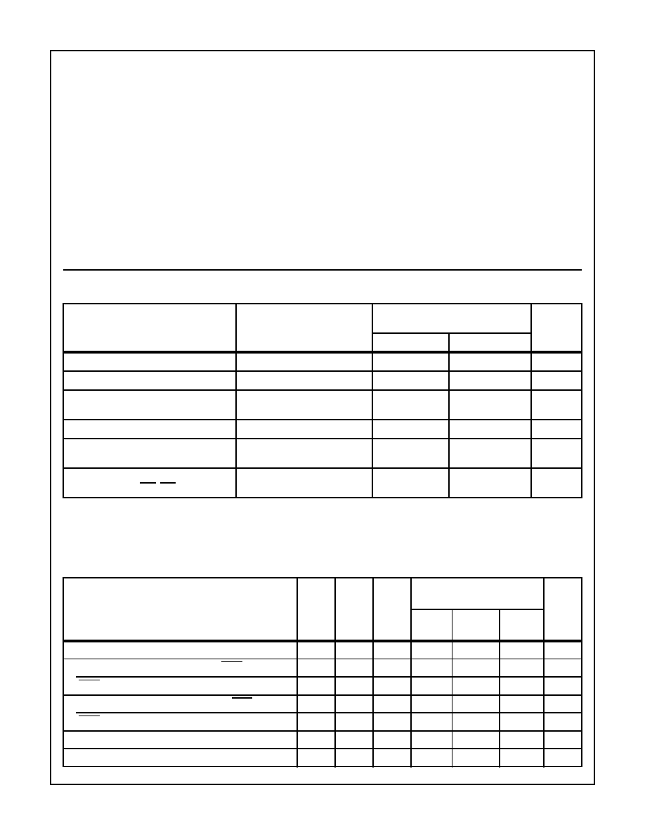
Recommended Operating Conditions
T
A
= Full-Package Temperature Range. For maximum reliability, operating conditions
should be selected so that operation is always within the following ranges.
PARAMETER
TEST CONDITIONS
V
DD
(V)
CDP1805ACD, CDP1805ACE
CDP1806ACD, CDP1806ACE
UNITS
MIN
MAX
DC Operating Voltage Range
-
4
6.5
V
Input Voltage Range
-
V
SS
V
DD
V
Minimum Instruction Time (Note 1)
(f
CL
= 5MHz)
5
3.2
-
µ
s
Maximum DMA Transfer Rate
5
-
0.625
Mbyte/s
Maximum Clock Input Frequency,
Load Capacitance (C
L
) = 50pF
5
DC
5
MHz
Maximum External Counter/Timer Clock
Input Frequency to EF1, EF2
5
DC
2
MHz
NOTES:
1. Equals 2 machine cycles - one Fetch and one Execute operation for all instructions except Long Branch, Long Skip, NOP, and "68" family
instructions, which are more than two cycles.
2.
JA
is measured with the component mounted on an evaluation PC board in free air.
Static Electrical Specifications
at T
A
= -40
o
C to +85
o
C, V
DD
±
5%, Except as Noted
PARAMETER
V
O
(V)
V
IN
(V)
V
DD
(V)
CDP1805ACD, CDP1805ACE
CDP1806ACD, CDP1806ACE
UNITS
MIN
(NOTE 3)
TYP
MAX
Quiescent Device Current, I
DD
-
0, 5
5
-
50
200
µ
A
Output Low Drive (Sink) Current, (Except XTAL), I
OL
0.4
0, 5
5
1.6
4
-
mA
XTAL Output, I
OL
0.4
5
5
0.2
0.4
-
mA
Output High Drive (Source) Current (Except XTAL, I
OH
4.6
0, 5
5
-1.6
-4
-
mA
XTAL, I
OH
4.6
0
5
-0.1
-0.2
-
mA
Output Voltage Low Level, V
OL
-
0, 5
5
-
0
0.1
V
Output Voltage High Level, V
OH
-
0, 5
5
4.9
5
-
V
CDP1805AC, CDP1806AC

5
Input Low Voltage (BUS0 - BUS7, ME), V
IL
0.5, 4.5
-
5
-
-
1.5
V
Input High Voltage (BUS0 - BUS7, ME), V
IH
0.5, 4.5
-
5
3.5
-
-
V
Schmitt Trigger Input Voltage (Except BUS0 - BUS7, ME)
Positive Trigger Threshold, V
P
0.5, 4.5
-
5
2.2
2.9
3.6
V
Negative Trigger Threshold, V
N
0.5, 4.5
-
5
0.9
1.9
2.8
V
Hysteresis, V
H
0.5, 4.5
-
5
0.3
0.9
1.6
V
Input Leakage Current, I
IN
-
0, 5
5
-
±
0.1
±
5
µ
A
Three-State Output Leakage Current, I
OUT
0, 5
0, 5
5
-
±
0.2
±
5
µ
A
Input Capacitance, C
IN
-
-
-
-
5
7.5
pF
Output Capacitance, C
OUT
-
-
-
-
10
15
pF
Total Power Dissipation (Note 4)
Run
-
-
5
-
35
50
mW
Idle "00" at M (0000)
-
-
5
-
12
18
mW
Minimum Data Retention Voltage, V
DR
V
DD
= V
DR
-
2
2.4
V
Data Retention Current, I
DR
V
DD
= 2.4
-
25
100
µ
A
NOTES:
3. Typical values are for T
A
= +25
o
C and nominal V
DD
.
4. External clock: f = 5MHz, t
R
, t
F
= 10ns; C
L
= 50pF.
Dynamic Electrical Specifications
at T
A
= -40
o
to +85
o
C; C
L
= 50pF; Input t
R
, t
F
= 10ns; Input Pulse Levels = 0.1V to
V
DD
-0.1V; V
DD
= 5V,
±
5%.
PARAMETER
CDP1805AC CDP1806AC
UNITS
(NOTE 5)
TYP
MAX
Propagation Delay Times
Clock to TPA, TPB, t
PLH
, t
PHL
150
275
ns
Clock-to-Memory High-Address Byte, t
PLH
, t
PHL
325
550
ns
Clock-to-Memory Low-Address Byte, t
PLH
, t
PHL
275
450
ns
Clock to MRD, t
PLH
, t
PHL
200
325
ns
Clock to MWR, t
PLH
, t
PHL
(See Note 5)
150
275
ns
Clock to (CPU DATA to BUS), t
PLH
, t
PHL
375
625
ns
Clock to State Code, t
PLH
, t
PHL
225
400
ns
Clock to Q, t
PLH
, t
PHL
250
425
ns
Clock to N, t
PLH
, t
PHL
250
425
ns
Clock to Internal RAM Data to BUS, t
PLH
, t
PHL
420
650
ns
Static Electrical Specifications
at T
A
= -40
o
C to +85
o
C, V
DD
±
5%, Except as Noted (Continued)
PARAMETER
V
O
(V)
V
IN
(V)
V
DD
(V)
CDP1805ACD, CDP1805ACE
CDP1806ACD, CDP1806ACE
UNITS
MIN
(NOTE 3)
TYP
MAX
CDP1805AC, CDP1806AC

