4-5
CDP1851,
CDP1851C
CMOS Programmable I/O Interface
Description
THE CDP1851 and CDP1851C are CMOS programmable two-
port I/Os designed for use as general-purpose I/O devices.
They are directly compatible with CDP1800-series micropro-
cessors functioning at maximum clock frequency. Each port
can be programmed in either byte-I/O or bit-programmable
modes for interfacing with peripheral devices such as printers
and keyboards.
Both ports A and B can be separately programmed to be 8-bit
input or output ports with handshaking control lines, RDY and
STROBE. Only port A can be programmed to be a bidirectional
port. This configuration provides a means for communicating
with a peripheral device or microprocessor system on a single
8-bit bus for both transmitting and receiving data. Handshaking
signals are provided to maintain proper bus access control.
Port A handshaking lines are used for input control and port B
handshaking lines are used for output; therefore port B must be
in the bit-programmable mode where handshaking is not used.
Ports A and B can be separately bit programmed so that each
individual line can be designated as an input or output line. The
handshaking lines may also be individually programmed as
input or output when port A is not in bidirectional mode.
The CDP1851 has a supply-voltage range of 4V to 10.5V, and
the CDP1851C has a range of 4V to 6.5V. Both types are sup-
plied in 40-lead dual-in-line plastic (E suffix) or hermetic
ceramic (D suffix) packages. The CDP1851C is also available
in chip form (H suffix).
Features
∑ 20 Programmable I/O Lines
∑ Programmable for Operation in Four Modes:
- Input
- Output
- Bidirectional
- Bit-programmable
∑ Operates in Either I/O or Memory Space
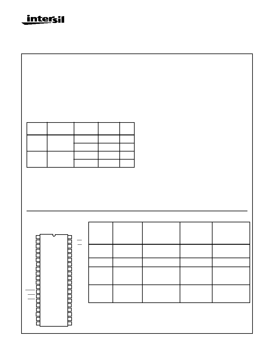
Ordering Information
PACKAGE TEMP. RANGE
5V
10V
PKG.
NO.
PDIP
-40
o
C to +85
o
C CDP1851CE
CDP1851E
E40.6
Burn-In
CDP1851CEX
-
E40.6
SBDIP
-40
o
C to +85
o
C CDP1851CD
-
D40.6
Burn-In
CDP1851CDX CDP1851DX D40.6
March 1997
File Number
1056.2
Pinout
CDP1851, CDP1851C
(PDIP, SBDIP)
TOP VIEW
13
1
2
3
4
5
6
7
8
9
10
11
12
14
15
16
17
18
19
20
CLOCK
CS
RA0
RA1
BUS0
BUS1
BUS2
BUS3
BUS4
BUS5
BUS6
BUS7
CLEAR
A INT
B INT
B RDY
B
B0
B1
V
SS
28
40
39
38
37
36
35
34
33
32
31
30
29
27
26
25
24
23
22
21
V
DD
RD/WE
WR/RE
TPB
A RDY
A
A0
A1
A2
A3
A4
A5
A6
A7
B7
B6
B5
B4
B3
B2
STROBE
STROBE
CDP1851 Programming Modes
MODE
(8)
PORT A
DATA PINS
(2)
PORT A
HANDSHAKING
PINS
(8)
PORT B
DATA PINS
(2)
PORT B
HANDSHAKING
PINS
Input
Accept Input
Data
READY, STROBE
Accept Input Data
READY, STROBE
Output
Output Data
READY, STROBE
Output Data
READY, STROBE
Bidirectional
(Port A Only)
Transfer In-
put/Output Data
Input Handshaking
for Port A
Must be Previous-
ly Set to Bit-Pro-
grammable Mode
Output Handshaking
for Port A
Bit-Program-
mable
Programmed In-
dividually as In-
puts or Outputs
Programmed Individ-
ually as Inputs or
Outputs
Programmed Indi-
vidually as Inputs
or Outputs
Programmed Individ-
ually as Inputs or
Outputs
CAUTION: These devices are sensitive to electrostatic discharge; follow proper IC Handling Procedures.
http://www.intersil.com or 407-727-9207
|
Copyright
©
Intersil Corporation 1999
4-6
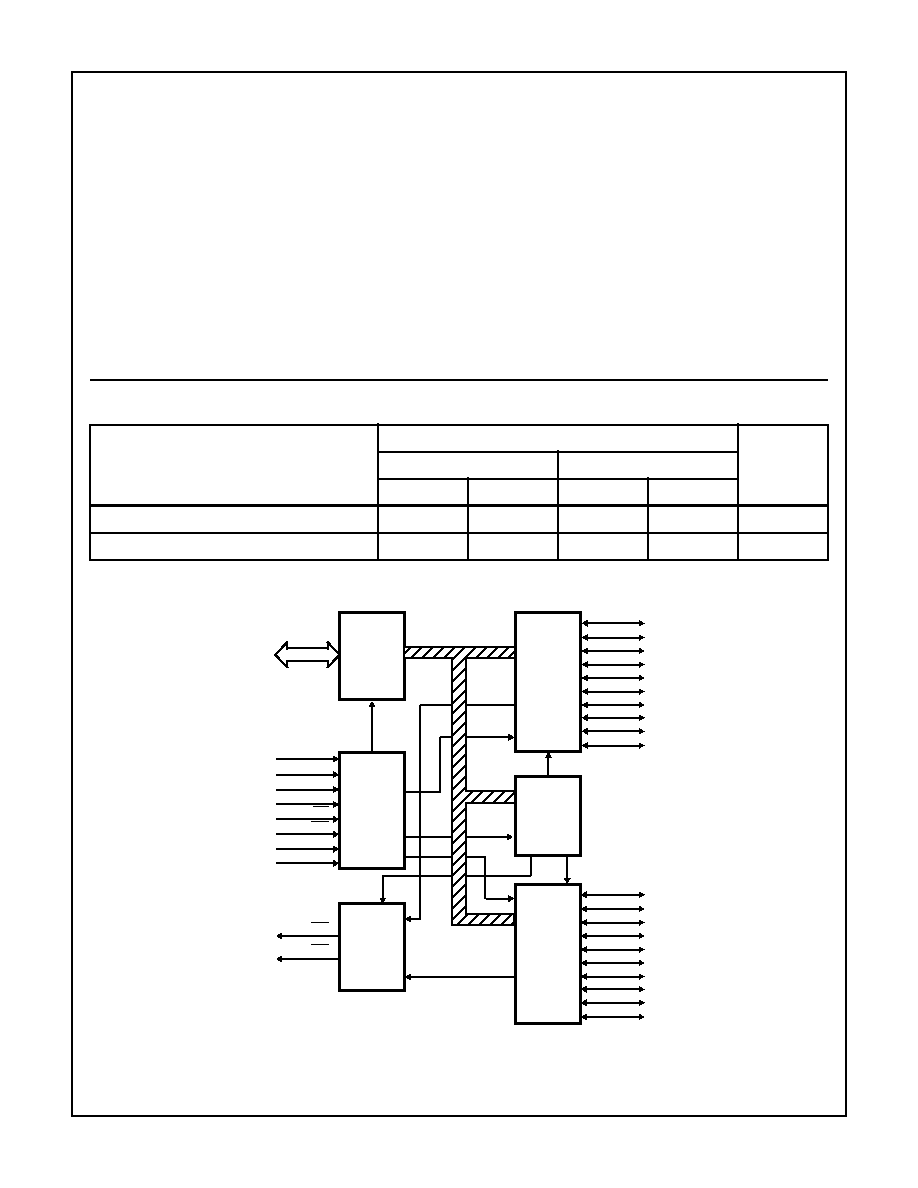
Functional Diagram
Absolute Maximum Ratings
Thermal Information
DC Supply-Voltage Range, (V
DD
)
(Voltage Referenced to V
SS
Terminal)
CDP1851 . . . . . . . . . . . . . . . . . . . . . . . . . . . . . . . . . . -0.5 to+11V
CDP1851C . . . . . . . . . . . . . . . . . . . . . . . . . . . . . . . . . .-0.5 to +7V
Input Voltage Range, All Inputs . . . . . . . . . . . . . . -0.5 to V
DD
+0.5V
DC Input Current, Any One Input
. . . . . . . . . . . . . . . . . . . . . . . . .±
10mA
Device Dissipation Per Output Transistor
For T
A
= Full Package-Temperature Range
(All Package Type) . . . . . . . . . . . . . . . . . . . . . . . . . . . . . . . 40mW
Operating-Temperature Range (T
A
)
Package Type D, H . . . . . . . . . . . . . . . . . . . . . . . -55
o
C to +125
o
C
Package Type E . . . . . . . . . . . . . . . . . . . . . . . . . . -40
o
C to +85
o
C
Thermal Resistance (Typical, Note 1)
JA
(
o
C/W)
JC
(
o
C/W)
PDIP Package . . . . . . . . . . . . . . . . . . .
50
N/A
SBDIP Package . . . . . . . . . . . . . . . . . .
36
12
Maximum Storage Temperature Range (T
STG
) . . . . -65
o
C to +150
o
C
Maximum Lead Temperature (During Soldering)
At Distance 1/16
±
1/32 inch (1.59
±
0.79mm)
from Case for 10s max . . . . . . . . . . . . . . . . . . . . . . . . . . . +265
o
C
CAUTION: Stresses above those listed in "Absolute Maximum Ratings" may cause permanent damage to the device. This is a stress only rating and operation
of the device at these or any other conditions above those indicated in the operational sections of this specification is not implied.
NOTE:
1.
JA
is measured with the component mounted on an evaluation PC board in free air.
Operating Conditions
At T
A
= Full Package-Temperature Range. For Maximum Reliability, Operating Conditions Should be
Selected so that Operation is Always within the Following Ranges:
PARAMETER
LIMITS
UNITS
CDP1851
CDP1851C
MIN
MAX
MIN
MAX
DC Operating Voltage Range
4
10.5
4
6.5
V
Input Voltage Range
V
SS
V
DD
V
SS
V
DD
V
MODE
CONTROL
AND
STATUS
REGISTERS
B0
B1
B2
B3
B4
B5
B6
B7
READY
STROBE
SECTION
B
A0
A1
A2
A3
A4
A5
A6
A7
READY
STROBE
SECTION
A
CLOCK
CS
RA0
RA1
WR/RD
RD/WR
TPB
CLEAR
ADDRESS
DECODE
AND
READ/
WRITE
LOGIC
A INT
B INT
INTERRUPT
MASKING
AND
LOGIC
DATA
BUS
BUFFER
DATA
BUS
FIGURE 1. FUNCTIONAL DIAGRAM FOR CDP1851 AND CDP1851C
CDP1851, CDP1851C
4-7
Functional Description
The CDP1851 has four modes of operation: input, output,
bidirectional, and bit-programmable. Port A is programmable
in all modes; port B is programmable in all but the
bidirectional mode. A control byte must be loaded into the
control register to program the ports. In the input and output
modes, each port has two handshaking signals, STROBE
and RDY. In the bidirectional mode, port A has four
handshaking signals: A RDY and A STROBE for input, B
RDY and B STROBE for output. If port A is programmed in
the bidirectional mode, port B must be programmed in the
bit-programmable mode. Each terminal of port A or B may
be individually programmed for input or output in the bit-
programmable mode. Since handshaking is not used in this
mode, the RDY and STROBE lines may also be used for bit-
programming if port A is not in the bidirectional mode.
Input Mode
When a peripheral device has data to input, it sends a
STROBE pulse to the PlO. The leading edge of this pulse
clears the RDY line, inhibiting further transmission from the
peripheral. The trailing edge of the STROBE pulse latches the
data into the PlO buffer register and also activates the INT line
to signal the CPU to read this data. The lNT pin can be wired
to the INT pin of the CPU or the EF lines for polling. The CPU
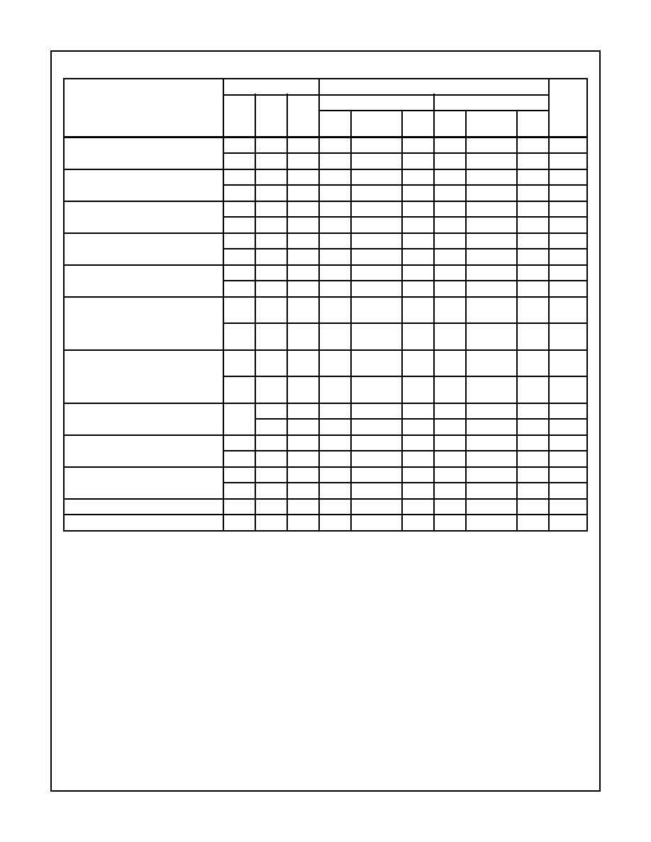
Static Electrical Specifications
At T
A
= -40
o
C to +85
o
C, V
DD
5%, Unless Otherwise Specified
PARAMETER
CONDITIONS
LIMITS
UNITS
V
O
(V)
V
IN
(V)
V
DD
(V)
CDP1851
CDP1851C
MIN
(NOTE1)
TYP
MAX
MIN
(NOTE1)
TYP
MAX
Quiescent Device Current
I
DD
-
0, 5
5
-
0.01
50
-
0.02
200
µ
A
-
0, 10
10
-
1
200
-
-
-
µ
A
Output Low Drive
(Sink) Current
I
OL
0.4
0, 5
5
1.6
3.2
-
1.6
3.2
-
mA
0.5
0, 10
10
2.6
5.2
-
-
-
-
mA
Output High Drive
(Source) Current
I
OH
4.6
0, 5
5
-1.15
-2.3
-
-1.15
-2.3
-
mA
9.5
0, 10
10
-2.6
-5.2
-
-
-
-
mA
Output Voltage Low-Level
(Note 2)
V
OL
-
0, 5
5
-
0
0.1
-
0
0.1
V
-
0, 10
10
-
0
0.1
-
-
-
V
Output Voltage High Level
(Note 2)
V
OH
-
0, 5
5
4.9
5
-
4.9
5
-
V
-
0, 10
10
9.9
10
-
-
-
-
V
Input Low Voltage
V
IL
0.5,
4.5
-
5
-
-
1.5
-
-
1.5
V
0.5,
9.5
-
10
-
-
3
-
-
-
V
Input High Voltage
V
lH
0.5,
4.5
-
5
3.5
-
-
3.5
-
-
V
0.5,
9.5
-
10
7
-
-
-
-
-
V
Input Leakage Current
I
lN
Any
Input
0, 5
5
-
-
±
1
-
-
±
1
µ
A
0, 10
10
-
-
±
2
-
-
-
µ
A
Three-State Output Leakage
Current
I
OUT
0, 5
0, 5
5
-
-
±
1
-
-
±
1
µ
A
0, 10
0, 10
10
-
-
±
1
-
-
-
µ
A
Operating Current (Note 3)
I
DD1
-
0, 5
5
-
1.5
3
-
1.5
3
mA
-
0, 10
10
-
6
12
-
-
-
mA
Input Capacitance
C
IN
-
-
-
-
5
7.5
-
5
7.5
pF
Output Capacitance
C
OUT
-
-
-
-
10
15
-
10
15
pF
NOTES:
1. Typical values are for T
A
= 25
o
C and nominal V
DD
.
2. I
OL
= I
OH
= 1
µ
A
3. Operating current is measured at 200kHz for V
DD
= 5V and 400kHz for V
DD
= 10V, with open output (worst-case frequencies for
CDP1802A system operating at maximum speed of 3.2MHz).
CDP1851, CDP1851C
4-8
then executes an input or a load instruction, depending on the
mapping technique used. In either case the proper code must
be asserted on the RAO, RA1, and CS lines to read the buffer
register (see Table 6).
The INT line is deactivated on the leading edge of TPB. The
trailing edge of TPB sets the RDY line to signal the periph-
eral that the port is ready to be loaded with new data. If RDY
is low when the input mode is entered (i.e. after a reset), a
"dummy" read must be done to set RDY high and signal the
peripheral device that the port is ready to be loaded.
Output Mode
A peripheral STROBE pulse sent to the PlO generates an
interrupt to signal the CPU that the peripheral device is
ready for data. The CPU executes the proper output or store
instruction. Data are then read from memory and placed on
the bus. The data are latched into the port buffer at the end
of the window when RE/WE = 0 and WR/RE = 1. The RDY
line is also set at this time, indicating to the peripheral that
there is data in the port buffer. The INT line is deactivated at
the beginning of the window. After the peripheral reads valid
port data, it can send another STROBE pulse, clearing the
RDY line and activating the INT line as in the input mode.
Bidirectional Mode
This mode programs port A to function as both an input and
output port. The bidirectional feature allows the peripheral to
control port direction by using both sets of handshake signals.
The port A handshaking pins are used to control input data
from peripheral to PlO, while the port B handshaking pins are
used to control output data from PlO to peripheral. Data are
transferred in the same manner as the input and output
modes. Since A INT is used for both input and output, the sta-
tus register must be read to determine what condition caused
A INT to be activated (see Table 5).
Bit-Programmable Mode
This mode allows individual bits of port A or port B to be
programmed as inputs or outputs. To output data to bits
programmed as outputs, the CPU loads a data byte into the
8-bit port as in the output mode (no handshaking). Only bits
programmed for outputs latch this data. Data must be stable
when reading from bits programmed as inputs, since the
input bits do not latch. When the CDP1851 inputs data to the
CPU the CPU also reads the output bits latched during the
last output cycle. The RDY and STROBE lines may be used
for I/O by using the STROBE/RDY I/O control byte in Table 2.
An additional feature available in the bit-programmable
mode is the ability to generate interrupts based on
input/output byte combinations. These interrupts can be
programmed to occur on logic conditions (AND, OR, NAND,
and NOR) generated by the eight I/O lines of each port (The
STROBE and RDY lines cannot generate interrupts).
A0
A1
A2
A3
A4
A5
A6
A7
INT
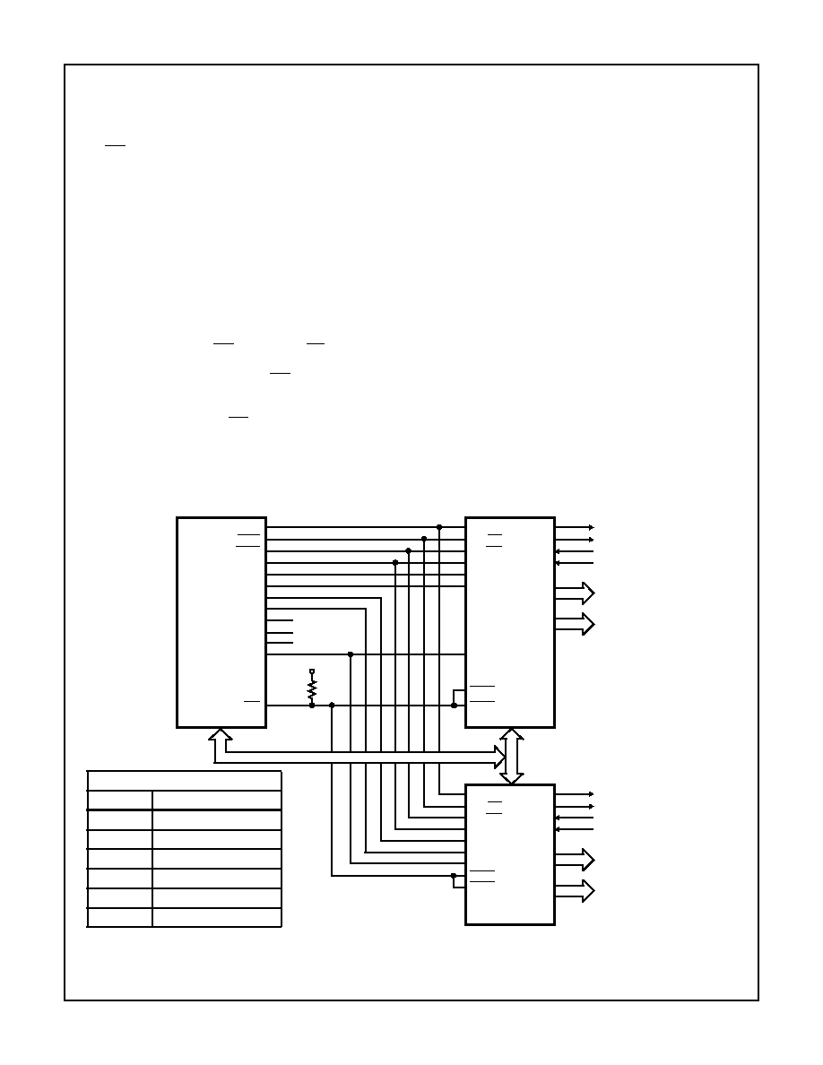
BUS 0-7
CDP1800
FAMILY
µ
P
TPA
MWR
MRD
TPB
V
DD
10k
RA0
RA1
A RDY
PORT A0 - A7
PORT B0 - B7
A INT
BUS 0-7
PIO
NO. 1
CLOCK
RD/WE
WR/RE
TPB
CDP1851
B INT
CS
B RDY
A STROBE
B STROBE
RA0
RA1
A RDY
PORT A0 - A7
PORT B0 - B7
PIO
NO. 2
CLOCK
RD/WE
WR/RE
TPB
CDP1851
B RDY
A STROBE
B STROBE
CS
A INT
B INT
ADDRESS REGISTER
ADDRESS
SELECTS
8001
No. 1 Control/Status Reg
8002
No. 1 Port A
8003
No. 1 Port B
8004
No. 2 Control/Status Reg
8008
No. 2 Port A
800C
No. 2 Port B
FIGURE 2. MEMORY SPACE I/O. THIS CONFIGURATION ALLOWS UP TO FOUR CDP1851s TO OCCUPY MEMORY SPACE 8XXX WITH
NO ADDITIONAL HARDWARE (A4-A5 AND A6-A7 ARE USED AS RA0 AND RA1 ON THE THIRD AND FOURTH PIO's)
CDP1851, CDP1851C

4-9
Programming
Initialization and Controls
The CDP1851 PlO must be cleared by a low on the CLEAR
input during power-on to set it for programming. Once
programmed, modes can be changed without clearing
except when exiting the bit-programmable mode. A low on
the CLEAR input sets both ports to the input modes,
disables interrupts, unmasks all bit-programmed interrupt
bits, and resets the status register, A RDY, and B RDY.
Mode Setting
The control register must be sequentially loaded with the
appropriate mode set control bytes in order as shown in Table
1 (i.e. input mode then output mode, etc.). Port A is set with
the SET A bit = 1 and port B is set with the SET B bit = 1. If a
port is set to the bit-programmable mode, the bit-programming
control byte from Table 2 must be loaded. A bit is programmed
for output with the I/O bit = 1 and for input with the I/O bit = 0.
The STROBE and RDY lines may be programmed for input or
output with the STROBE/RDY control byte of Table 2. Input
data on the STROBE and RDY lines is detected by reading
the status register. When using the STROBE or RDY lines for
output, the control byte must be loaded every time output data
is to be changed. To program logical conditions that will gen-
erate an interrupt, the interrupt control byte of Table 3 must be
loaded. An interrupt mask of the eight I/O lines may be loaded
next, if bit D4 (mask follows) of the interrupt control byte = 1.
The I/O lines are masked if the corresponding bit of the inter-
rupt mask register is 1, otherwise it is monitored. Any combi-
nation of masked bits are permissible, except all bits masked
(mask = FF).
INT Enable Disable
To enable or disable the INT line in all modes, the interrupt
ENABLE/DISABLE byte must be loaded (see Table 4). Inter-
rupts can also be detected by reading the status register
(see Table 5). All interrupts should be disabled when
programming or false interrupts may occur. The INT outputs
are open drain NMOS devices that allow wired O Ring (use
10K pull-up registers).
SET PORTS A AND B
TO INPUT, OUTPUT, OR
BIT-PROGRAMMABLE MODE
USING TABLE 1
GENERATE CLEAR PULSE
AT PIN 13
IS
EITHER PORT
SET TO THE
BIT-PROGRAMMABLE
MODE 3
NO
YES
NOW SET PORT A TO
BIDIRECTIONAL MODE,
IF DESIRED
SET MASTER INTERRUPT
ENABLE/DISABLE
USING TABLE 4
MAIN PROGRAM
WILL
INTERRUPTS
BE USED FOR
BIT-PROGRAMMED
PORT?
PERFORM FOLLOWING
SEQUENCE BEFORE
PROGRAMMING PORT A TO
BIDIRECTIONAL MODE
SET BIT DIRECTION
USING TABLE 2
SET BIT LOGICAL
CONDITIONS AND
MASKING USING
TABLE 3
REPEAT FOR EACH
BIT-PROGRAMMABLE
PORT
REPEAT FOR EACH
BIT-PROGRAMMABLE
PORT
YES
NO
FIGURE 3. A FLOW CHART GUIDE TO CDP1851 MODE PROGRAMMING
NOTES:
1. STROBE/READY I/O Control Byte (Table 2) is also used to output data to STROBE and READY lines when bit-programmed.
2. Status register (Table 2) is used to input data from STROBE and READY lines when bit-programmed.
3. Interrupt status is also read from status register.
CDP1851, CDP1851C