 | –≠–ª–µ–∫—Ç—Ä–æ–Ω–Ω—ã–π –∫–æ–º–ø–æ–Ω–µ–Ω—Ç: CDP1853C | –°–∫–∞—á–∞—Ç—å:  PDF PDF  ZIP ZIP |

4-40
Features
∑ Provides Direct Control of Up to 7 Input and 7 Output
Devices When used with a CDP1800-Series Micropro-
cessor
∑ CHIP ENABLE (CE) Allows Easy Expansion for Multi-
level I/O Systems
Description
The CDP1853/3 and CDP1853C/3 are high-reliability 1 of 8
decoders designed for use in general purpose microproces-
sor systems. These devices, which are functionally identical,
are specifically designed for use as gated N-bit decoders
and interface directly with the 1800-Series microprocessors
without additional components. The CDP1853/3 has a rec-
ommended operating voltage range of 4V to 10.5V, and the
CDP1853C/3 has a recommended operating voltage range
of 4V to 6.5V.
When CHIP ENABLE (CE) is high, the selected output will be
true (high) from the trailing edge of CLOCK A (high-to-low
transition) to the trailing edge of CLOCK B (high-to-low
transition). All outputs will be low when the device is not
selected (CE = 0) and during conditions of CLOCK A and
CLOCK B as shown in Figure 2. The CDP1853/3 inputs N0,
N1, N2, CLOCK A, and CLOCK B are connected to 1800-
series microprocessor outputs N0, N1, N2, TPA, and TPB
respectively, when used to decode I/O commands as shown
in Figure 5. The CHIP ENABLE (CE) input provides the capa-
bility for multiple levels of decoding as shown in Figure 6.
The CDP1853/3 can also be used as a general purpose 1 of
8 decoder for I/O and memory system applications as shown
in Figure 4.
Pinout
16 LEAD SBDIP
TOP VIEW
Ordering Information
PACKAGE
TEMP. RANGE
5V
10V
PKG.
NO.
SBDIP
-55
o
C to +125
o
C CDP1853CD3
-
D16.3
14
15
16
9
13
12
11
10
1
2
3
4
5
7
6
8
CLK A
N0
N1
OUT 0
OUT 1
OUT 2
V
SS
OUT 3
V
DD
N2
CE
OUT 4
OUT 5
OUT 6
OUT 7
CLK B
March 1997
File Number
1713.2
CDP1853C/3
High-Reliability CMOS N-Bit 1 of 8 Decoder
CAUTION: These devices are sensitive to electrostatic discharge; follow proper IC Handling Procedures.
http://www.intersil.com or 407-727-9207
|
Copyright
©
Intersil Corporation 1999

4-41
CDP1853/3 Functional Diagram
FIGURE 1.
TRUTH TABLE
NOTES:
1. 1 = High level, 0 = Low level, X = Don't care.
2. Qn-1 = Enable remains in previous state.
QN
4
5
6
7
12
11
10
9
1 OF 8
DECODER
OUT 0
OUT 1
OUT 2
OUT 3
OUT 4
OUT 5
OUT 6
OUT 7
2
3
14
N0
N1
N2
13
CE
1
15
CLOCK
A
CLOCK
B
(TPA)
(TPB)
EN
CE
CL A
CL B
EN
1
0
0
Qn-1(Note 2)
1
0
1
1
1
1
0
0
1
1
1
1
0
X
X
0
N2
N1
N0
EN
0
1
2
3
4
5
6
7
0
0
0
1
1
0
0
0
0
0
0
0
0
0
1
1
0
1
0
0
0
0
0
0
0
1
0
1
0
0
1
0
0
0
0
0
0
1
1
1
0
0
0
1
0
0
0
0
1
0
0
1
0
0
0
0
1
0
0
0
1
0
1
1
0
0
0
0
0
1
0
0
1
1
0
1
0
0
0
0
0
0
1
0
1
1
1
1
0
0
0
0
0
0
0
1
X
X
X
0
0
0
0
0
0
0
0
0
CDP1853/3, CDP1853C/3

4-42
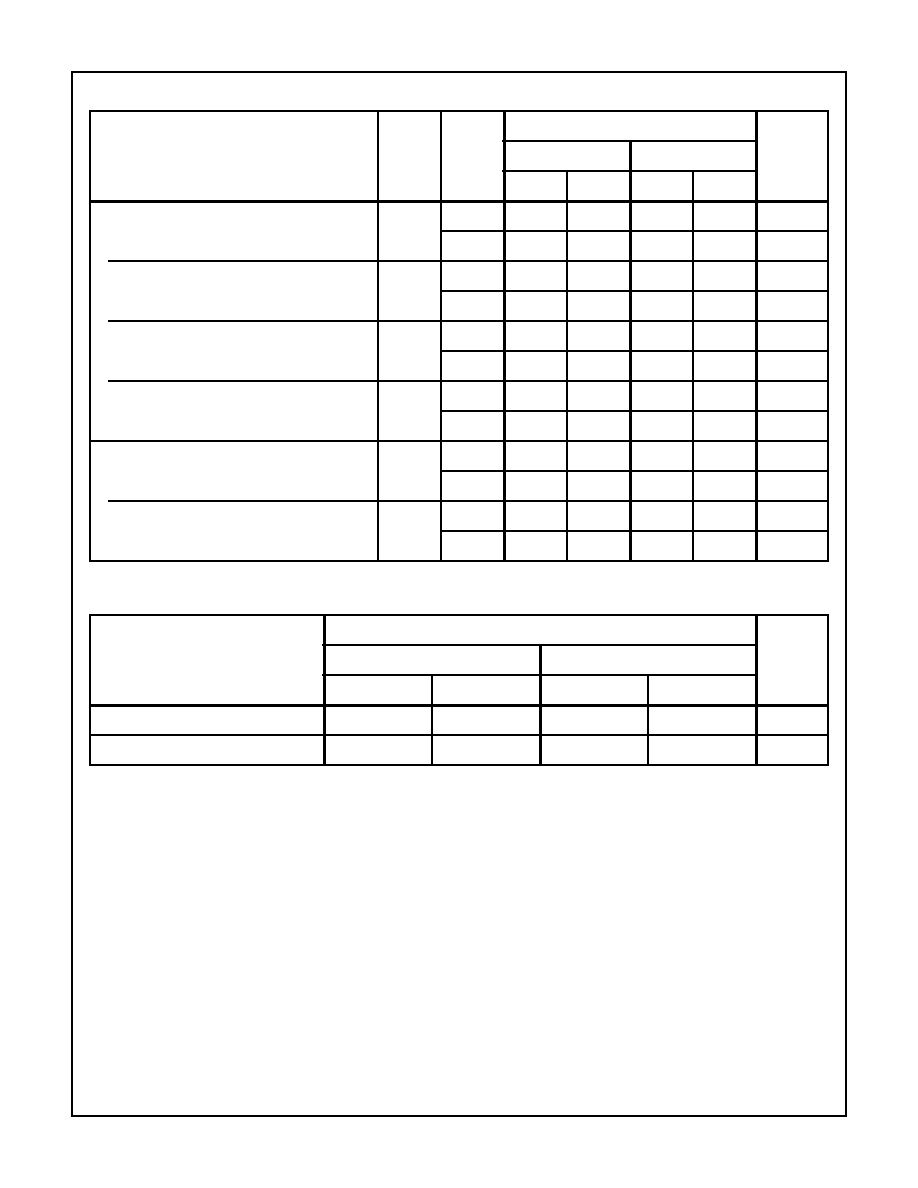
Static Electrical Specifications
PARAMETER
SYMBOL
CONDITIONS
LIMITS
UNITS
V
O
(V)
V
IN
(V)
V
DD
(V)
-55
o
C, +25
o
C
+125
o
C
MIN
MAX
MIN
MAX
Quiescent Device
Current
I
SS
(Note 1)
-
0, 5
5
-50
-
-100
-
µ
A
-
0, 10
10
-500
-
-1000
-
µ
A
Output Low Drive
(Sink) Current
I
OL
0.4
-
5
2.3
-
1.6
-
mA
0.5
-
10
3.7
-
2.6
-
mA
Output High Drive
(Source) Current
I
OH
4.6
-
5
-
-1.7
-
-1.2
mA
9.5
-
10
-
-3.7
-
-2.6
mA
Output Voltage
Low-Level
V
OL
(Note 2)
-
0, 5
5
-
0.1
-
0.2
V
-
0, 10
10
-
0.1
-
0.2
V
Output Voltage
High-Level
V
OH
(Note 2)
-
0, 5
5
4.9
-
4.8
-
V
-
0, 10
10
9.9
-
9.8
-
V
Input Low Voltage
V
IL
0.8, 4.2
-
5
-
1.5
-
1.5
V
1, 9
-
10
-
3
-
3
V
Input High Voltage
V
IH
0.8, 4.2
-
5
3.5
-
3.5
-
V
1, 9
-
10
7
-
7
-
V
Input Leakage Low
I
IL
-
0
5
-1
-
-5
-
µ
A
-
0
10
-1
-
-5
-
µ
A
Input Leakage High
I
IH
-
5
5
-
1
-
5
µ
A
-
10
10
-
1
-
5
µ
A
Input Capacitance
C
IN
(Note 2)
-
-
-
-
10
-
10
pF
Output Capacitance
C
OUT
(Note 2)
-
-
-
-
15
-
15
pF
NOTES:
1. The CDP1853C meets all 5V static electrical characteristics of the CDP1853 except quiescent device current for which the limits are:
I
SS
= -500
µ
A at -55
o
C and +25
o
C and I
SS
= -1000
µ
A at +125
o
C.
2. Guaranteed but not tested.
Dynamic Electrical Specifications
See Figure 2, C
L
= 100pF, t
R
, t
F
= 15ns
PARAMETER
SYMBOL
V
DD
(V)
LIMITS
UNITS
-55
o
C, +25
o
C
+125
o
C
MIN
MAX
MIN
MAX
Propagation Delay Time:
t
EOH
5
-
175
-
275
ns
Chip Enable (CE) to Output High
10
-
90
-
150
ns
CDP1853/3, CDP1853C/3
4-43
Disable to Output Low
t
EOL
5
-
295
-
400
ns
10
-
200
-
250
ns
N Input to Output
t
NO
5
-
225
-
315
ns
10
-
120
-
165
ns
Clock A to Output Low
t
AO
5
-
210
-
300
ns
10
-
110
-
150
ns
Clock B to Output Low
t
BO
5
-
295
-
400
ns
10
-
200
-
250
ns
Pulse Width:
t
CACA
5
50
-
75
-
ns
Clock A
10
25
-
50
-
ns
Clock B
t
CBCB
5
50
-
75
-
ns
10
25
-
50
-
ns
Recommended Operating Conditions
At T
A
= Full Package Temperature Range. For maximum reliability, operating conditions
should be selected so that operation is always within the following ranges:
PARAMETER
LIMITS
UNITS
CDP1853/3
CDP1853C/3
MIN
MAX
MIN
MAX
DC Operating Voltage Range
4
10.5
4
6.5
V
Input voltage Range
V
SS
V
DD
V
SS
V
DD
V
Dynamic Electrical Specifications
See Figure 2, C
L
= 100pF, t
R
, t
F
= 15ns
PARAMETER
SYMBOL
V
DD
(V)
LIMITS
UNITS
-55
o
C, +25
o
C
+125
o
C
MIN
MAX
MIN
MAX
CDP1853/3, CDP1853C/3

4-44
Absolute Maximum Ratings
Thermal Information
DC Supply Voltage Range, (V
DD
)
(All Voltages Referenced to V
SS
Terminal)
CDP1853/3 . . . . . . . . . . . . . . . . . . . . . . . . . . . . . . . -0.5V to +11V
CDP1853C/3. . . . . . . . . . . . . . . . . . . . . . . . . . . . . . . -0.5V to +7V
Input Voltage Range, All Inputs . . . . . . . . . . . . . -0.5V to V
DD
+0.5V
DC Input Current, Any One Input . . . . . . . . . . . . . . . . . . . . .
±
10mA
Thermal Resistance (Typical)
JA
(
o
C/W)
JC
(
o
C/W)
SBDIP Package . . . . . . . . . . . . . . . . . .
85
22
Device Dissipation Per Output Transistor
T
A
= Full Package Temperature Range
(All Package Types) . . . . . . . . . . . . . . . . . . . . . . . . . . . . . . 100mW
Operating Temperature Range (T
A
)
Package Type D. . . . . . . . . . . . . . . . . . . . . . . . . .-55
o
C to +125
o
C
Storage Temperature Range (T
STG
). . . . . . . . . . . .-65
o
C to +150
o
C
Lead Temperature (During Soldering)
At distance 1/16
±
1/32 In. (1.59
±
0.79mm)
from case for 10s max . . . . . . . . . . . . . . . . . . . . . . . . . . . . +265
o
C
Timing Diagrams
FIGURE 2A. N - INPUTS TO OUTPUTS DELAY TIME
FIGURE 2B. CE TO OUTPUT DELAY TIME
FIGURE 2C. CLOCK B TO OUTPUT DELAY TIME
NOTE:
1. To measure T
AO
, Clock B must be tied low.
FIGURE 2D. CLOCK A TO OUTPUT DELAY TIME
FIGURE 2. PROPAGATION DELAY TIME DIAGRAMS
NOTE:
1. Output enabled when EN = high. Internal signal shown for refer-
ence only (see Figure 1).
FIGURE 3. TIMING DIAGRAM
FIGURE 4. N-BIT DECODER USED AS A 1 OF 8 DECODER
N0 - N2
OUTPUT 0 - 7
T
N0
CE
OUTPUT 0 - 7
T
EOH
T
EOL
MIN. CLOCK B
OUTPUT 0 - 7
T
BO
CLOCK B
PULSE WIDTH
T
CBCB
T
AO
CLOCK A
OUTPUT 0 - 7
MIN. CLOCK A
PULSE WIDTH
T
CACA
(SEE NOTE 1)
TPA
TPB
CE
EN
OUTPUT
(NOTE 1)
A
B
C
CHIP ENABLE
V
DD
CLK A
N0
N1
OUT 0
OUT 1
OUT 2
OUT 3
N2
CE
OUT 4
OUT 5
OUT 6
OUT 7
CLK B
CDP1853/3, CDP1853C/3