 | –≠–ª–µ–∫—Ç—Ä–æ–Ω–Ω—ã–π –∫–æ–º–ø–æ–Ω–µ–Ω—Ç: CDP1855D | –°–∫–∞—á–∞—Ç—å:  PDF PDF  ZIP ZIP |

4-47
Features
∑ Cascadable Up to 4 Units for 32-Bit by 32-Bit Multiply
or 64
˜
32-Bit Divide
∑ 8-Bit by 8-Bit Multiply or 16
˜
8-Bit Divide in 5.6
µ
s at
5V or 2.8
µ
s at 10V
∑ Direct Interface to CDP1800-Series Microprocessors
∑ Easy Interface to Other 8-Bit Microprocessors
∑ Significantly Increases Throughput of Microprocessor
Used for Arithmetic Calculations
Description
The CDP1855 and CDP1855C are CMOS 8-bit multi-
ply/divide units which can be used to greatly increase the
capabilities of 8-bit microprocessors. They perform multiply
and divide operations on unsigned, binary operators. In
general, microprocessors do not contain multiply or divide
instructions and even efficiently coded multiply or divide
subroutines require considerable memory and execution
time. These multiply/divide units directly interface to the
CDP1800-series microprocessors via the N-lines and can
easily be configured to fit in either the memory or I/O space
of other 8-bit microprocessors.
The multiple/divide unit is based on a method of multiplying
by add and shift right operations and dividing by subtract and
shift left operations. The device is structured to permit cas-
cading identical units to handle operands up to 32 bits.
The CDP1855 and CDP1855C are functionally identical.
They differ in that the CDP1855 has a recommended
operating voltage range of 4V to 10.5V, and the CDP1855C,
a recommended operating voltage range of 4V to 6.5V.
The CDP1855 and CDP1855C types are supplied in a 28
lead hermetic dual-in-line ceramic package (D suffix) and in
a 28 lead dual-in-line plastic package (E suffix). The
CDP1855C is also available in chip form (H suffix).
Ordering Information
PACKAGE TEMP. RANGE
5V
10V
PKG.
NO.
PDIP
-40
o
C to +85
o
C CDP1855CE
CDP1855E E28.6
Burn-In
CDP1855CEX
-
E28.6
SBDIP
-40
o
C to +85
o
C CDP1855CD CDP1855D D28.6
Burn-In
CDP1855CDX
-
D28.6
Pinout
28 LEAD DIP
TOP VIEW
Circuit Configuration
CE
CLEAR
CTL
C.O./O.F.
Y
L
Z
L
SHIFT
CLK
STB
RD/WE
RA2
RA1
RA0
V
SS
V
DD
CN1
CI
Y
R
Z
R
BUS 6
BUS 4
BUS 3
BUS 2
BUS 1
BUS 0
CN0
BUS 7
BUS 5
28
27
26
25
24
23
22
21
20
19
18
17
16
15
1
2
3
4
5
6
7
8
9
10
11
12
13
14
CLEAR
XTAL
N0
N1
N2
TPB
MRD
CDP1802
BUS
EF
CLEAR
CLK
RA0
RA1
RA2
STB
RD/WE
CDP1855
BUS
C0
Y
L
Z
R
CTL
Y
R
Z
L
CE
C1
CN0
CN1
+V
FIGURE 1. MDU ADDRESSED AS I/O DEVICE
March 1997
CDP1855,
CDP1855C
8-Bit Programmable
Multiply/Divide Unit
File Number
1053.2
CAUTION: These devices are sensitive to electrostatic discharge; follow proper IC Handling Procedures.
http://www.intersil.com or 407-727-9207
|
Copyright
©
Intersil Corporation 1999
4-48
Absolute Maximum Ratings
Thermal Information
DC Supply Voltage Range, (V
DD
)
(All voltage values referenced to V
SS
terminal)
CDP1855 . . . . . . . . . . . . . . . . . . . . . . . . . . . . . . . . -0.5V to +11V
CDP1855C. . . . . . . . . . . . . . . . . . . . . . . . . . . . . . . . -0.5V to +7V
Input Voltage Range, All Inputs . . . . . . . . . . . . . -0.5V to V
DD
+0.5V
DC Input Current, Any One Input
. . . . . . . . . . . . . . . . . . . . . . . . .±
10mA
Thermal Resistance (Typical)
JA
(
o
C/W)
JC
(
o
C/W)
PDIP Package . . . . . . . . . . . . . . . . . . .
55
N/A
SBDIP Package . . . . . . . . . . . . . . . . . .
50
12
Device Dissipation Per Output Transistor
For T
A
= Full Package-Temperature Range
(All Package Types) . . . . . . . . . . . . . . . . . . . . . . . . . . . . . . 100mW
Operating Temperature Range (T
A
) . . . . . . . . . . . . .-40
o
C to +85
o
C
Storage Temperature Range (T
STg
) . . . . . . . . . . . .-65
o
C to +150
o
C
Lead Temperature (During Soldering)
At distance 1/16
±
1/32 In. (1.59
±
0.79mm)
from case for 10s max . . . . . . . . . . . . . . . . . . . . . . . . . . . . +265
o
C
CAUTION: Stresses above those listed in "Absolute Maximum Ratings" may cause permanent damage to the device. This is a stress only rating and operation
of the device at these or any other conditions above those indicated in the operational sections of this specification is not implied.
Static Electrical Specifications
At T
A
= -40 to +85
o
C, V
DD
±
10%, Unless Otherwise Specified
PARAMETER
CONDITIONS
LIMITS
UNITS
V
O
(V)
V
IN
(V)
V
DD
(V)
CDP1855
CDP1855C
MIN
(NOTE1)
TYP
MAX
MIN
(NOTE1)
TYP
MAX
Quiescent Device
Current
I
DD
-
0, 5
5
-
0.01
50
-
0.02
200
µ
A
-
0, 10
10
-
1
200
-
-
-
µ
A
Output Low Drive (Sink)
Current
I
OL
0.4
0, 5
5
1.6
3.2
-
1.6
3.2
-
mA
0.5
0, 10
10
2.6
5.2
-
-
-
-
mA
Output High Drive
(Source) Current
I
OH
4.6
0, 5
5
-1.15
-2.3
-
-1.15
-2.3
-
mA
9.5
0, 10
10
-2.6
-5.2
-
-
-
-
mA
Output Voltage Low Level
(Note 2)
V
OL
-
0, 5
5
-
0
0.1
-
0
0.1
V
-
0, 10
10
-
0
0.1
-
-
-
V
Output Voltage High Level
(Note 2)
V
OH
-
0, 5
5
4.9
5
-
4.9
5
-
V
-
0, 10
10
9.9
10
-
-
-
-
V
Input Low Voltage
V
IL
0.5, 4.5
-
5
-
-
1.5
-
-
1.5
V
0.5, 9.5
-
10
-
-
3
-
-
-
V
Input High Voltage
V
IH
0.5, 4.5
-
5
3.5
-
-
3.5
-
-
V
0.5, 9.5
-
10
7
-
-
-
-
-
V
Input Leakage Current
I
IN
-
0, 5
5
-
-
±
1
-
-
±
1
µ
A
-
0, 10
10
-
-
±
1
-
-
-
µ
A
Three-State Output
Leakage Current
I
OUT
0, 5
0, 5
5
-
-
±
1
-
-
±
1
µ
A
0, 10
0, 10
10
-
-
±
10
-
-
-
µ
A
Operating Current
(Note 3)
I
DD1
-
0, 5
5
-
1.5
-
-
1.5
3
mA
-
0, 10
10
-
6
12
-
-
-
mA
Input Capacitance
C
IN
-
-
-
-
5
7.5
-
5
7.5
pF
Output Capacitance
C
OUT
-
-
-
-
10
15
-
10
15
pF
NOTES:
1. Typical values are for T
A
= +25
o
C and nominal V
DD
.
2. I
OL
= I
OH
= 1
µ
A
3. Operating current is measured at 3.2MHz with open outputs.
CDP1855, CDP1855C

4-49
Recommended Operating Conditions
At T
A
= Full package temperature range. For maximum reliability, operating conditions
should be selected so that operation is always within the following ranges:
PARAMETER
V
DD
(V)
LIMITS
UNITS
CDP1855
CDP1855C
MIN
MAX
MIN
MAX
DC Operating Voltage Range
-
4
10.5
4
6.5
V
Input Voltage Range
-
V
SS
V
DD
V
SS
V
DD
V
Maximum Clock Input Frequency
5
3.2
-
3.2
-
MHz
10
6.4
-
-
-
MHz
Minimum 8 x 8 Multiply (16
˜
8 Divide) Time
5
-
5.6
-
5.6
µ
s
10
-
2.8
-
-
µ
s
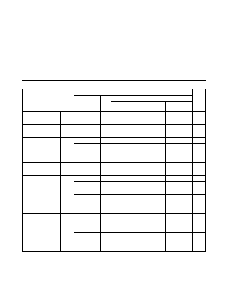
FIGURE 2. BLOCK DIAGRAM OF CDP1855 AND CDP1855C
22
BUS
7
21
BUS
6
20
BUS
5
19
BUS
4
18
BUS
3
17
BUS
2
16
BUS
1
15
BUS
0
11
REGISTER
SELECT LOGIC
12
13
1
SELECT CONTROL
SELECT Z
SELECT Y
SELECT X
SELECT STATUS
X SEQUENCE
COUNTER
RESET
OUT
8
CLOCK
26
CN1
27
CN0
8
ADD/
SUBTRACT
X REGISTER
LOAD
8
SHIFT
GENERATOR
Y REGISTER
LOAD
STATUS
REG
8
8
Y SEQUENCE
COUNTER
RESET
OUT
Z SEQUENCE
COUNTER
RESET
OUT
CHIP
NO.
SHIFT
RESET
Z REGISTER
LOAD
8
SHIFT
RESET
25
3
4
5
24
6
23
LOAD
10
7
2
9
CONTR
OL
REGISTER
RD/WE
SHIFT
CLEAR
STB
C.I.
CTL.
C.O./O.F.
Y
L
Y
R
Z
L
Z
R
RA2 RA1 RA0
CE
C.O.
14
28 V
DD
V
SS
CDP1855, CDP1855C

4-50
Functional Description
The CDP1855 is a multiply-divide unit (MDU) designed to be
compatible with CDP1800 series microprocessor systems. It
can, in fact, be interfaced to most 8-bit microprocessors (see
Figure 5). The CDP1855 performs binary multiply or divide
operations as directed by the microprocessor. It can do a
16N-bit by 8N-bit divide yielding a 8N-bit result plus and 8N-
bit remainder. The multiply is an 8N-bit by 8N-bit operation
with a 16N-bit result. The "N" represent the number of
cascaded CDP1855's and can be 1, 2, 3 or 4. All operations
require 8N + 1 shift pulses (See "DELAY NEEDED WITH
AND WITHOUT PRESCALER").
The CDP1855 contains three registers, X, Y, and Z, which
are loaded with the operands prior to an operation and
contain the results at the completion. In addition, the control
register must be loaded to initiate a multiply or divide. There
is also a status register which contains an overflow flag as
shown in the "CONTROL REGISTER BIT ASSIGNMENT
TABLE". The register address lines (RA0-RA1) are used to
select the appropriate register for loading or reading. The
RD/WE and STB lines are used in conjunction with the RA
lines to determine the exact MDU response (See
"CONTROL TRUTH TABLE").
When multiple MDU's are cascaded, the loading of each reg-
ister is done sequentially. For example, the first selection of
register X for loading loads the most significant CDP1855,
the second loads the next significant, and so on. Registers
are also read out sequentially. This is accomplished by inter-
nal counters on each MDU which are decremented by STB
during each register selection. When the counter matches
the chip number (CN1, CN0 lines), the device is selected.
These counters must be cleared with a clear on pin 2 or with
bit 6 in the control word (See "CONTROL REGISTER BIT
ASSIGNMENT TABLE") in order to start each sequence of
accesses with the most significant device.
The CDP1855 has a built in clock prescaler which can be
selected via bit 7 in the control register. The prescaler may
be necessary in cascaded systems operating at high
frequencies or in systems where a suitable clock frequency
is not readily available. Without the prescaler select, the shift
frequency is equal to the clock input frequency. With the
prescaler selected, the rate depends on the number of
MDU's as defined by bits 4 and 5 of the control word (See
"CONTROL REGISTER BIT ASSIGNMENT TABLE").
1. For one MDU, the clock frequency is divided by 2.
2. For two MDU's the clock frequency is divided by 4.
3. For 3 or 4 MDU's, the clock frequency is divided by 8.
Operation
1. Initialization and Controls
The CDP1855 must be cleared by a low on pin 2 during
power-on which prevents bus contention problems at the Y
L
,
Y
R
and Z
L
, Z
R
terminals and also resets the sequence
counters and the shift pulse generator.
Prior to loading any other registers the control register must
be loaded to specify the number of MDU's being used (See
"CONTROL REGISTER BIT ASSIGNMENT TABLE").
Once the number of devices has been specified and the
sequence counters cleared with a clear pulse or bit 6 of the
control word, the X, Y, and Z registers can be loaded as
defined in the "CONTROL TRUTH TABLE". All bytes of the X
register can be loaded, then all bytes of the Y, and then all
bytes of the Z, or they can be loaded randomly. Successive
loads to a given register will always proceed sequentially
from the most significant byte to the least significant byte, as
previously described. Resetting the sequence counters
select the most significant MDU. In a four MDU system, load-
ing all MDU's results in the sequence counter pointing to the
first MDU again. In all other configurations (1, 2, or 3
MDU's), the sequence counter must be reset prior to each
series of register reads or writes.
2. Divide Operation
For the divide operation, the divisor is loaded in the X
register. The dividend is loaded in the Y and Z registers with
the more significant half in the Y register and the less signifi-
cant half in the Z register. These registers may be loaded in
any order, and after loading is completed, a control word is
loaded to specify a divide operation and the number of
MDU's and also to reset the sequence counters and Y or Z
register and select the clock option if desired. Clearing the
sequence counters with bit 6 will set the MDU's up for read-
ing the results.
The X register will be unaltered by the operation. The
quotient will be in the Z register while the remainder will be in
the Y register. An overflow will be indicated by the C.O./O.F.
of the most significant MDU and can also be determined by
reading the status byte.
While the CDP1855 is specified to perform 16 by 8-bit
divides, if the quotient of a divide operation exceeds the size
of the Z register(s) (8N-bits - where N is the number of
cascaded CDP1855's) the overflow bit in the Status Register
will be set. Neither the quotient in Z nor the remainder in Y
will represent a valid answer. This will always be the result of
a division performed when the divisor (X) is equal to or less
than the most significant 8N-bits of the dividend (Y).
The MDU can still be used for such computations if the
divide is done in two steps. The dividend is split into two
parts-the more significant 8N-bits and the less significant
8N-bits-and a divide done on each part. Each step yields an
8N-bit result for a total quotient of 16N-bits.
The first step consists of dividing the more significant 8N-
bits by the divisor. This is done by clearing the Y register(s),
loading the Z register(s) with the more significant 8N-bits of
the dividend, and loading the X register(s) with the divisor. A
division is performed and the resultant value in Z represents
the more significant 8N-bits of the final quotient. The Z regis-
ter(s) value must be unloaded and saved by the processor.
CDP1855, CDP1855C
4-51
A second division is performed using the remainder from the
first division (in Y) as the more significant 8N-bits of the divi-
dend and the less significant half of the original dividend
loaded into the Z register. The divisor in X remains unaltered
and is, by definition, larger than the remainder from the first
division which is in Y. The resulting value in Z becomes the
less significant 8N-bits of the final quotient and the value in Y
is, as usual, the remainder.
Extending this technique to more steps allows division of any
size number by an 8N-bit divisor.
Note that division by zero is never permitted and must be
tested for and handled in software.
The following example illustrates the use of this algorithm.
Example:
Assume three MDU's capable of a by 24-bit division. The
problem is to divide 00F273, 491C06H by 0003B4H.
The Z register can simply be reset using bit 2 of the control
word and another divide can be done in order to further
divide the remainder.
3. Multiply Operation
For a multiply operation the two numbers to be multiplied are
loaded in the X and Z registers. The result is in the Y and Z
register with Y being the more significant half and Z the less
significant half. The X register will be unchanged after the
operation is completed.
The original contents of the Y register are added to the
product of X and Z. Bit 3 of the control word will reset
register Y to 0 if desired.
Functional Description of
CDP1855 Terminals
CE - Chip Enable (Input):
A high on this pin enables the CDP1855 MDU to respond to
the select lines. All cascaded MDU's must be enabled
together. CE also controls the three-state C.O./O.F., output
of the most significant MDU.
Clear (Input):
The CDP1855 MDU(s) must be cleared upon power-on with
a low-on this pin. The clear signal resets the sequence
counters, the shift pulse generator, and bits 0 and 1 of the
control register.
CTL - Control (Input):
This is an input pin. All CTL pins must be wired together and
to the Y
L
of the most significant CDP1855 MDU and to the
Z
R
of the least significant CDP1855 MDU. This signal is
used to indicate whether the registers are to be operated on
or only shifted.
C.O./O.F. - Carry Out/Over Flow (Output):
This is a three-state output pin. It is the CDP1855 Carry Out
signal and is connected to Cl (CARRY-IN) of the next more
significant CDP1855 MDU, except for on the most significant
MDU. On that MDU it is an overflow indicator and is enabled
when chip enables is true. A low on this pin indicates that an
overflow has occurred. The overflow signal is latched each
time the control register is loaded, but is only meaningful
after a divide command.
Y
L
, Y
R
- Y-Left, Y-Right:
These are three-state bi-directional pins for data transfer
between the Y registers of cascaded CDP1855 MDU's. The
Y
R
pin is an output and Y
L
is an input during a multiply and
the reverse is true at all other times. The Y
L
pin must be
connected to the Y
R
pin of the next more significant MDU.
An exception is that the Y
L
pin of the most significant
CDP1855 MDU must be connected to the Z
R
pin of the least
significant MDU and to the CTL pins of all MDU's. Also the
Y
R
pin of the least significant MDU is tied to the Z
L
pin of the
most significant MDU.
Z
L
, Z
R
- Z-Left, Z-Right:
These are three-state bi-directional pins for data transfers
between the "Z" registers of cascaded MDU's. The Z
R
pin is
an output and Z
L
is an input during a multiply and the
reverse is true at all other times. The Z
L
pin must be tied to
the Y
R
pin of the next more significant MDU. An exception is
that the Z
L
in of the most significant MDU must be con-
nected to the Y
R
pin of the least significant MDU. Also, the
Z
R
pin of the least significant MDU is tied to the Y
L
of the
most significant MDU.
Shift - Shift Clock:
This is a three-state bi-directional pin. It is an output on the
most significant MDU. And an input on all other MDU's. It
provides the MDU system timing pulses. All SHIFT pins must
be connected together for cascaded operation. A maximum
of the 8N +1 shifts are required for an operation where "N"
equals the number of MDU devices that are cascaded.
CLK - Clock (Input):
This pin should be grounded on all but the most significant
MDU. There is an optional reduction of clock frequency avail-
able on this pin if so desired, controlled by bit 7 of the control
byte.
STB - Strobe (Input):
When RD/WE is low, data is latched from bus lines on the
falling edge of this signal. It may be asynchronous to the
clock. Strobe also increments the selected register's
sequence counter during reads and writes. TPB would be
used in CDP1800 systems.
Step 1:
000000
,
00F273
/
0003B4
=
000041
R=0001BF
Y
Z(MS)
X
Z1
Y1
Step 2: 0001BF
,
491C06
/
0003B4
=
78C936
R=00000E
Y1
Z(LS)
X
Z2
Y2
Result:
000041
,
78C936
R=00000E
Z1
Z2
Y2
CDP1855, CDP1855C