
4-76
CDP1872C,
CDP1874C, CDP1875C
High-Speed 8-Bit Input and Output Ports
Description
The CDP1872C, CDP1874C and CDP1875C devices are
high-speed 8-bit parallel input and output ports designed for
use in the CDP1800 microprocessor system and for general
use in other microprocessor systems. The CDP1872C and
CDP1874C are 8-bit input ports; the CDP1875C is an 8-bit
output port.
These devices have flexible capabilities as buffers and data
latches and are reset by CLR input when the data strobe is
not active.
The CDP1872C and CDP1874C are functionally identical
except for device selects.The CDP1872C has one active low
and one active high select; the CDP1874C has two active
high device selects. These devices also feature Three-state
outputs when deselected. Data is strobed into the register on
the leading edge of the CLOCK and latched on the trailing
edge of the CLOCK.
The CDP1875C is an output port with data latched into the
registers when the device selects are active. There are two
active high and one active low selects. The output buffers
are enabled at all times.
Features
∑ Parallel 8-Bit Input/Output Register with Buffered Out-
puts
∑ High-Speed Data-In to Data-Out 85ns (Max) at V
DD
= 5V
∑ Flexible Applications In Microprocessor Systems as
Buffers and Latches
∑ High Order Address-Latch Capability in CDP1800-
Series Microprocessor Systems
∑ Output Sink Current = 5mA (Min) at V
DD
= 5V
∑ Three-State Output - CDP1872C and CDP1874C
Ordering Information
PART
NUMBER
TEMP. RANGE
PACKAGE
PKG.
NO.
CDP1872CE
-40
o
C to +85
o
C
PDIP
E22.4
CDP1874CE
-40
o
C to +85
o
C
PDIP
E22.4
CDP1875CE
-40
o
C to +85
o
C
PDIP
E22.4
March 1997
File Number
1255.2
CDP1874C INPUT PORT
(PDIP)
TOP VIEW
1
11
10
9
8
7
6
5
3
2
4
22
12
13
14
15
16
17
18
19
21
20
DI0
DO0
DI1
D01
DI2
D02
D03
DI3
CLOCK
V
SS
DI7
DI6
D06
DI5
D07
D05
DI4
D04
CLR
CS2
CS1
V
DD
CDP1875C OUTPUT PORT
(PDIP)
TOP VIEW
1
11
10
9
8
7
6
5
3
2
4
22
12
13
14
15
16
17
18
19
21
20
DI0
DO0
DI1
D01
DI2
D02
D03
DI3
CS3
V
SS
DI7
DI6
D06
DI5
D07
D05
DI4
D04
CLR
CS2
CS1
V
DD
Pinouts
CDP1872C INPUT PORT
(PDIP)
TOP VIEW
1
11
10
9
8
7
6
5
3
2
4
22
12
13
14
15
16
17
18
19
21
20
DI0
DO0
DI1
D01
DI2
D02
D03
DI3
CLOCK
V
SS
DI7
DI6
D06
DI5
D07
D05
DI4
D04
CLR
CS2
CS1
V
DD
CAUTION: These devices are sensitive to electrostatic discharge; follow proper IC Handling Procedures.
http://www.intersil.com or 407-727-9207
|
Copyright
©
Intersil Corporation 1999

4-77
Absolute Maximum Ratings
Thermal Information
DC Supply Voltage Range, (V
DD
) . . . . . . . . . . . . . . . . . -0.5V to +7V
(Voltage referenced to V
SS
Terminal)
Input Voltage Range, All Inputs . . . . . . . . . . . . . -0.5V to V
DD
+0.5V
DC Input Current, Any One Input
. . . . . . . . . . . . . . . . . . . . . . . . .±
10mA
Thermal Resistance (Typical)
JA
(
o
C/W)
PDIP Package . . . . . . . . . . . . . . . . . . . . . . . . . . . . .
75
Device Dissipation Per Output Transistor
T
A
= Full Package Temperature Range
(All Package Types) . . . . . . . . . . . . . . . . . . . . . . . . . . . . . . 100mW
Operating Temperature Range (T
A
)
Package Type E . . . . . . . . . . . . . . . . . . . . . . . . . . . -40
o
C to +85
o
C
Storage Temperature Range (T
STG
) . . . . . . . . . . . . -65
o
C to +150
o
C
Lead Temperature (During Soldering)
At distance 1/16
±
1/32 In. (1.59
±
0.79mm)
from case for 10s max . . . . . . . . . . . . . . . . . . . . . . . . . . . . +265
o
C
CAUTION: Stresses above those listed in "Absolute Maximum Ratings" may cause permanent damage to the device. This is a stress only rating and operation
of the device at these or any other conditions above those indicated in the operational sections of this specification is not implied.
Recommended Operating Conditions
At T
A
= -40 to +85
o
C. For maximum reliability, operating conditions should be selected
so that operation is always within the following ranges:
PARAMETER
LIMITS
ALL TYPES
UNITS
DC Operating-Voltage Range
4 to 6.5
V
Input Voltage Range
V
SS
to V
DD
V
Static Electrical Specifications
At T
A
= -40 to +85
o
C, V
DD
±
5%, Unless Otherwise Specified.
PARAMETER
TEST CONDITIONS
LIMITS
ALL TYPES
UNITS
V
O
(V)
V
IN
(V)
V
DD
(V)
MIN
(NOTE 1)
TYP
MAX
Quiescent Device Current
I
DD
-
0, 5
5
-
25
50
µ
A
Output Low Drive (Sink)
Current
I
OL
0.4
0, 5
5
5
10
-
mA
Output High Drive (Source)
Current
I
OH
4.6
0, 5
5
-4
-7
-
mA
Output Voltage Low-Level
(Note 2)
V
OL
-
0, 5
5
-
0
0.1
V
Output Voltage High-Level
(Note 2)
V
OH
-
0, 5
5
4.9
5
-
V
Input Low Voltage
V
IL
0.5, 4.5
-
5
-
-
1.5
V
Input High Voltage
V
IH
0.5, 4.5
-
5
3.5
-
-
V
Input Leakage Current
I
IN
-
0, 5
5
-
-
±
1
µ
A
Three-State Output Leakage
Current (Note 3)
I
OUT
0, 5
0, 5
5
-
-
±
5
µ
A
Input Capacitance
C
IN
-
-
-
-
15
-
pF
Output Capacitance (Note 3)
C
OUT
-
-
-
-
15
-
pF
NOTES:
1. Typical values are for T
A
= +25
o
C and nominal V
DD
±
5%.
2. I
OL
= I
OH
= 1
µ
A
3. For CDP1872C and CDP1874C only.
CDP1872C, CDP1874C, CDP1875C
CDP1872C, CDP1874C, CDP1875C

4-78
Logic Diagrams
FIGURE 1. EQUIVALENT LOGIC DIAGRAM (1 OF 8 LATCHES
SHOWN) FOR CDP1872C
FIGURE 2. EQUIVALENT LOGIC DIAGRAM (1 OF 8 LATCHES
SHOWN) for CDP1874C
FIGURE 3. EQUIVALENT LOGIC DIAGRAM (1 OF 8 LATCHES SHOWN) FOR CDP1875C
Dynamic Electrical Specifications
At T
A
= 25
o
C, V
DD
5V, t
R
, t
F
= 10ns, V
IH
= 0.7V
DD
, V
IL
= 0.3V
DD
, C
L
= 150pF
PARAMETER
LIMITS
UNITS
CDP1872C, CDP1874C
MIN
(NOTE 1)
TYP
(NOTE 2)
MAX
INPUT PORT (FIGURE 4)
Output Enable
t
EN
-
45
90
ns
Output Disable
t
DIS
-
45
90
ns
Clock to Data Out
t
CLO
-
45
90
ns
Clear to Output
t
CRO
-
80
160
ns
Data In to Data Out
t
DIO
-
50
85
ns
Minimum Data Setup Time
t
DSU
-
10
30
ns
Data Hold Time
t
DH
-
10
30
ns
Minimum Clock Pulse Width
t
CL
-
30
60
ns
Minimum Clear Pulse Width
t
CR
-
30
60
ns
NOTES:
1. Typical values are for T
A
= +25
o
C and V
DD
±
5%.
2. Maximum values are for T
A
= +85
o
C and V
DD
±
5%
D
C
R
Q
CS1
CS2
DI
CLOCK
CLR
DO
D
C
R
Q
CS1
CS2
DI
CLOCK
CLR
DO
D
C
R
Q
CS1
CS3
CLR
DO
CS2
DI
CDP1872C, CDP1874C, CDP1875C
4-79
Dynamic Electrical Specifications
At T
A
= 25
o
C, V
DD
5V, t
R
, t
F
= 10ns, V
IH
= 0.7V
DD
, V
IL
= 0.3V
DD
, C
L
= 150pF
PARAMETER
LIMITS
UNITS
CDP1875C
MIN
(NOTE 1)
TYP
(NOTE 2)
MAX
OUTPUT PORT (FIGURE 5)
Clock to Data Out
t
CLO
-
50
100
ns
Clear to Output
t
CRO
-
80
160
ns
Data In to Data Out
t
DIO
-
50
85
ns
Minimum Data Setup Time
t
DS
-
10
30
ns
Data Hold Time
t
DH
-
10
30
ns
Minimum Clear Pulse Width
t
CR
-
30
60
ns
NOTES:
1. Typical values are for T
A
= +25
o
C and V
DD
±
5%.
2. Maximum values are for T
A
= +85
o
C and V
DD
±
5%
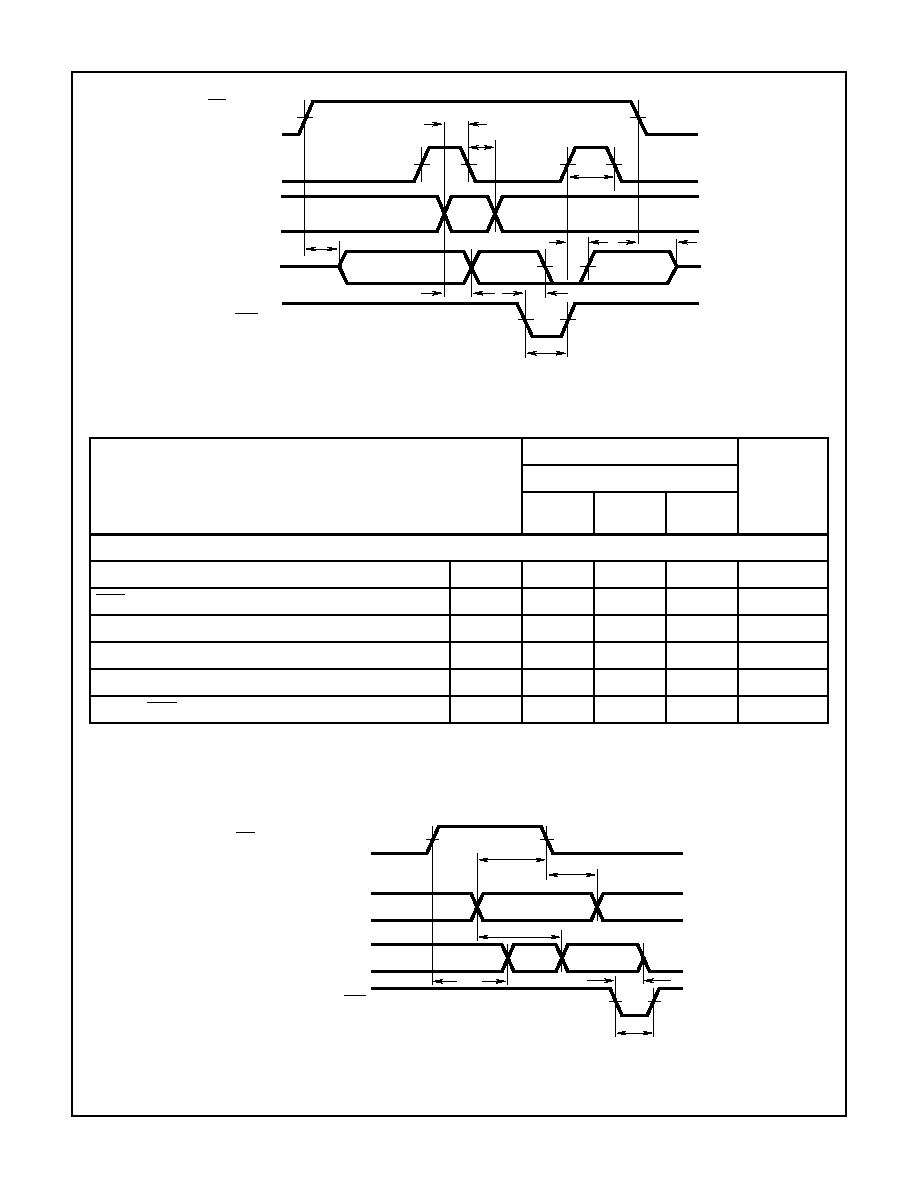
FIGURE 5. TIMING WAVEFORMS FOR CDP1875C (OUTPUT PORT)
t
CL
t
DIS
t
CRO
t
CR
t
DIO
t
DH
t
DSU
t
EN
CSI
∑
CS2
(CDP1872C)
CSI
∑
CS2
(CDP1874C)
CLOCK
DATA IN
DATA BUS
(HIGH Z)
CLR
t
CLO
FIGURE 4. TIMING WAVEFORMS FOR CDP1872C AND CDP1874C (INPUT-PORT TYPES)
t
CRO
t
CR
t
DIO
t
DH
t
DS
t
CLO
CSI
∑
CS2
∑
CS3 = CLOCK
DATA IN
CLR
DATA OUT
CDP1872C, CDP1874C, CDP1875C
