 | –≠–ª–µ–∫—Ç—Ä–æ–Ω–Ω—ã–π –∫–æ–º–ø–æ–Ω–µ–Ω—Ç: CDP1878CE | –°–∫–∞—á–∞—Ç—å:  PDF PDF  ZIP ZIP |

4-91
March 1997
Features
∑ Compatible with General Purpose and CDP1800
Series Microprocessor Systems
∑ Two 16-Bit Down Counters and Two 8-Bit Control
Registers
∑ 5 Modes Including a Versatile Variable-Duty Cycle
Mode
∑ Programmable Gate-Level Select
∑ Two-Complemented Output Pins for Each Counter-
Timer
∑ Software-Controlled Interrupt Output
∑ Addressable in Memory Space or CDP1800-Series I/O
Space
Description
The CDP1878C is a dual counter-timer consisting of two 16-
bit programmable down counters that are independently
controlled by separate control registers. The value in the reg-
isters determine the mode of operation and control func-
tions. Counters and registers are directly addressable in
memory space by any general industry type microproces-
sors, in addition to input/output mapping with the CDP1800
series microprocessors.
Each counter-timer can be configured in five modes with the
additional flexibility of gate-level control. The control regis-
ters in addition to mode formatting, allow software start and
stop, interrupt enable, and an optional read control that
allows a stable readout from the counters. Each counter-
timer has software control of a common interrupt output with
an interrupt status register indicating which counter-timer
has timed out.
In addition to the interrupt output, true and complemented
outputs are provided for each counter-timer for control of
peripheral devices.
This type is supplied in 28-lead dual-in-line ceramic pack-
ages (D suffix), and 28-lead dual-in-line plastic packages (E
suffix).
Pinout
CDP1878C
(DIP)
TOP VIEW
Ordering Information
PART
NUMBER
TEMP. RANGE
PACKAGE
PKG. NO.
CDP1878CE
-40
o
C to +85
o
C PDIP
E28.6
CDP1878CD
-40
o
C to +85
o
C SBDIP
N28.6
INT
TAO
TAO
TAG
TACL
RD
IO/MEM
TPB/WR
TPA
CS
A0
A1
A2
V
SS
V
DD
DB6
DB5
DB4
DB3
DB1
TBO
TBO
TBG
TBCL
RESET
DB7
DB2
DB0
28
27
26
25
24
23
22
21
20
19
18
17
16
15
1
2
3
4
5
6
7
8
9
10
11
12
13
14
TABLE 1. MODE DESCRIPTION
MODE
FUNCTION
APPLICATION
1 Timeout
Outputs change when clock
decrements counter to "0"
Event counter
2 Timeout
Strobe
One clockwide output pulse
when clock decrements
counter to "0"
Trigger pulse
3 Gate-Con-
trolled One
Shot
Outputs change when clock
decrements counter to "0".
Retriggerable
Time-delay
generation
4 Rate Generator Repetitive clockwide output
pulse
Time-base
generator
5 Variable-Duty
Cycle
Repetitive output with
programmed duty cycle
Motor control
File Number
1341.2
CDP1878C
CMOS Dual Counter-Timer
CAUTION: These devices are sensitive to electrostatic discharge; follow proper IC Handling Procedures.
http://www.intersil.com or 407-727-9207
|
Copyright
©
Intersil Corporation 1999

4-92
CDP1878C
Absolute Maximum Ratings
Thermal Information
DC Supply-Voltage Range, (V
DD
)
(All Voltages Referenced to V
SS
Terminal)
CDP1878C . . . . . . . . . . . . . . . . . . . . . . . . . . . . . . . . . -0.5V to +7V
Input Voltage Range, All Inputs . . . . . . . . . . . . . -0.5V to V
DD
+0.5V
DC Input Current, Any One Input
. . . . . . . . . . . . . . . . . . . . . . . . .±
10mA
Thermal Resistance (Typical)
JA
(
o
C/W)
JC
(
o
C/W)
PDIP Package . . . . . . . . . . . . . . . . . . .
55
N/A
SBDIP Package . . . . . . . . . . . . . . . . . .
50
12
Device Dissipation Per Output Transistor
T
A
= Full Package Temperature Range
(All Package Types) . . . . . . . . . . . . . . . . . . . . . . . . . . . . . . 100mW
Operating Temperature Range (T
A
)
Package Type D. . . . . . . . . . . . . . . . . . . . . . . . . .-55
o
C to +125
o
C
Package Type E . . . . . . . . . . . . . . . . . . . . . . . . . . .-40
o
C to +85
o
C
Storage Temperature Range (T
STG
). . . . . . . . . . . .-65
o
C to +150
o
C
Lead Temperature (During Soldering)
At distance 1/16
±
1/32 In. (1.59
±
0.79mm)
from case for 10s max . . . . . . . . . . . . . . . . . . . . . . . . . . . . +265
o
C
CAUTION: Stresses above those listed in "Absolute Maximum Ratings" may cause permanent damage to the device. This is a stress only rating and operation
of the device at these or any other conditions above those indicated in the operational sections of this specification is not implied.
Recommended Operating Conditions
At T
A
= Full Package Temperature Range. For maximum reliability, operating conditions
should be selected so that operation is always within the following ranges:
PARAMETER
SYMBOL
MIN
MAX
UNITS
DC Operating Voltage Range
4
6.5
V
Input Voltage Range
V
SS
V
DD
V
Maximum Clock Input Rise or Fall Time
t
R
, t
F
-
5
µ
s
Minimum Clock Pulse Width
t
WL
, t
WH
200
-
ns
Maximum Clock Input Frequency
f
CL
DC
1
MHz
Static Electrical Specifications
At T
A
= -40
o
C to +85
o
C, V
DD
±
5% Except as noted:
PARAMETER
SYMBOL
CONDITIONS
LIMITS
UNITS
V
O
(V)
V
IN
(V)
V
DD
(V)
MIN
(NOTE 1)
TYP
MAX
Quiescent Device Current
I
DD
-
0, 5
5
-
0.02
200
µ
A
Output Low Drive (Sink) Current
I
OL
0.4
0, 5
5
1.6
3.2
-
mA
Output High Drive (Source) Current
I
OH
4.6
0, 5
5
-1.15
-2.3
-
mA
Output Voltage Low-Level (Note 2)
V
OL
-
0, 5
5
-
0
0.1
V
Output Voltage High-Level (Note 2)
V
OH
-
0, 5
5
4.9
5
-
V
Input Low Voltage
V
IL
0.5, 4.5
-
5
-
-
1.5
V
Input High Voltage
V
IH
0.5, 9.5
-
5
3.5
-
-
V
Input Leakage Current
I
IN
Any Input
0, 5
5
-
-
±
1
µ
A
Operating Current (Note 3)
I
DD1
-
0, 5
5
-
1.5
3
mA
Input Capacitance
C
IN
-
-
-
-
5
7.5
pF
Output Capacitance
C
OUT
-
-
-
-
10
15
pF
NOTES:
1. Typical values are for T
A
= +25
o
C and nominal V
DD
.
2. I
OL
= I
OH
= 1
µ
A
3. Operating current measured at 200kHz for V
DD
= 5V, with open outputs (worst-case frequencies for CDP1802A system operating at max-
imum speed of 3.2MHz).

4-93
Functional Diagram
FUNCTIONAL DEFINITIONS FOR CDP1878C TERMINALS
TERMINAL
USAGE
TERMINAL
USAGE
V
DD
- V
SS
Power
TAO, TAO
Complemented outputs of Timer A
DB0-DB7
Data to and from device
TBO, TBO
Complemented outputs of Timer B
TPB/WR, RD
Directional Control Signals
TPA
Used with CDP1800-series processors, tied high
otherwise
A0, A1, A2
Addresses that select counters or registers
CS
Active high input that enables device
TACL, TBCL
Clocks used to decrement counters
INT
Low when counter is "0"
TAG, TBG
Gate inputs that control counters
RESET
When active, TAO, TBO are low, TAO, TBO are
high. Interrupt status register is cleared.
IO/MEM
Tied high in CDP1800 input/output mode, other-
wise tied low
RESET
RD
TPB/WR
IO/MEM
TPA
CS
A2
A1
A0
V
DD
V
SS
I-O
CONTROL
AND
LOGIC
DATA
BUS
DRIVERS
8-BIT
EXTERNAL
BUS
JAM
REGISTER A
HOLDING
REGISTER A
HOLDING
REGISTER B
JAM
REGISTER B
COUNTER A
COUNTER B
CONTROL REGISTER B
AND MODE CONTROL
INT AND
STATUS REGISTER
CONTROL REGISTER A
AND MODE CONTROL
INT
GATE A
TAO
TAO
CLOCK A
GATE B
TBO
TBO
CLOCK B
CDP1878C
4-94
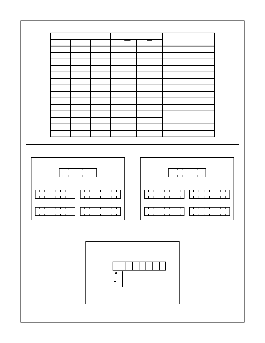
REGISTER TRUTH TABLE
ADDRESS
ACTIVE
REGISTER COUNTER
A2
A1
A0
TPB/WR
RD
1
1
0
X
Write Counter A MSB
1
1
0
X
Read Counter A MSB
0
1
0
X
Write Counter A LSB
0
1
0
X
Read Counter A LSB
1
0
0
X
Control Register A
1
1
1
X
Write Counter B MSB
1
1
1
X
Read Counter B MSB
0
1
1
X
Write Counter B LSB
0
1
1
X
Read Counter B LSB
1
0
1
X
Control Register B
1
0
0
X
Interrupt Status Register
1
0
1
X
0
0
0
Not Used
0
0
1
Not Used
Programming Model
COUNTER A REGISTERS
COUNTER B REGISTERS
INTERRUPT STATUS REGISTER
BUS 7
WRITE ONLY
BUS 0
CONTROL REGISTER
READ ONLY
HOLDING REGISTER LSB
HOLDING REGISTER MSB
WRITE ONLY
JAM REGISTER LSB
JAM REGISTER MSB
BUS 7
WRITE ONLY
BUS 0
CONTROL REGISTER
READ ONLY
HOLDING REGISTER LSB
HOLDING REGISTER MSB
WRITE ONLY
JAM REGISTER LSB
JAM REGISTER MSB
BUS 7
READ ONLY
BUS 0
TIMER A
TIMER B
X
X
0
0
0
0
0
0
CDP1878C

4-95
Functional DescriptIon
The dual counter-timer consists of two programmable 16-bit
down counters, separately addressable and controlled by
two independent 8-bit control registers. The word in the con-
trol register determines the mode and type of operation that
the counter-timer performs. Writing to or reading from a
counter or register is enabled by selective addressing during
a write or read cycle. The data is placed on the data bus by
the microprocessor during the write cycle or read from the
counter during the read cycle. Data to and from the counters
and to the control registers is in binary format.
Each counter-timer consists of three parts. The first is the
counter itself, a 16-bit down counter that is decremented on
the trailing edge of the clock input. The second is the jam
register that receives the data when the counter is written to.
The word in the control register determines when the jam
register value is placed into the counter. The third part is the
holding register that places the counter value on the data
bus when the counter is read.
When the counter has decremented to zero, three events
occur. The first involves the common interrupt output pin that,
if enabled, becomes active low. The second is the setting of a
bit in the interrupt status register. This register can be read to
determine which counter-timer has timed out. The third event
is the logic change of the complemented output pins.
In addition to the clock input used to decrement the counter, a
gate input is available to enable or initiate operation. The
counter-timers are independent and can have different mode
operations.
Write Operation
The counters and registers are separately addressable and
are programmed via the data bus when the chip is selected
with the TPB/WR pin active. Normal sequencing requires that
the counter jam register be loaded first with the required value
(most significant and least significant byte in any order), and
then the control register be accessed and loaded with the
control word. The trailing edge of the TPB/WR pulse will latch
the control word into the control register. The trailing edge of
the first clock to occur with gate valid will cause the counter to
be jammed with its initial value. The counter will decrement on
the trailing edge of succeeding clocks as long as the gate is
valid, until it reaches zero. The output levels will then change,
and if enabled, the interrupt output will become active and the
appropriate timer bit will be set in the interrupt status register.
The interrupt output and the interrupt status register can be
cleared (to their inactive state) by addressing the control reg-
ister with the TPB/WR line active For example, if counter A
times out, control register A must be accessed to reset the
interrupt output high and reset the timer A bit in the status reg-
ister low. Timer B bit in the status register will be unaffected.
Read Operation
Each counter has a holding register that is continuously
being updated by the counter and is accessed when the
counter is addressed during read cycles. Counter reads are
accomplished by halting the holding register and then read-
ing it, or by reading the holding register directly. If the holding
register is read directly, data will appear on the bus if the
counters are addressed with the RD line active. However, if
the clock decrements the counter between the two read
operations (most and least significant byte), an inaccurate
value will be read. To preclude this from happening, writing a
"1" into bit 6 of the control register and then addressing and
reading the counter will result in a stable reading. This oper-
ation prevents the holding register from being updated by the
counter and does not affect the counter's operation.
The interrupt status register is read by addressing either
control register with the RD line active. A "1" in bit 7 indicates
Timer A has timed out and a "1" in bit 6 indicates Timer B
has timed out. Bits 0-5 are zeros.
Control Register
Bits 0, 1 and 2
Mode Selects - See Mode Timing Diagrams (Figures 1, 2, 3,
4, and 5).
Note: When selecting a mode, the timer outputs TAO and TBO
are set low, and TAO and TBO are set high. If bits 0, 1 and 2
are all zero's when the control register is loaded, no mode is
selected, and the counter-timer outputs are unaffected. Issuing
mode 6 will cause an indeterminate condition of the counter,
issuing mode 7 is equivalent to issuing mode 5.
7
6
5
4
3
2
1
0
JAM ENABLE
1 = ENABLE
0 = DISABLE
HOLDING REGISTER CONTROL
1 = FREEZE HOLDING REGISTER
0 = UPDATE CONTINUOUSLY
START/STOP CONTROL
1 = START COUNTER
0 = STOP COUNTER
INTERRUPT ENABLE
1 = ENABLE
0 = DISABLE
GATE LEVEL SELECT
1 = POSITIVE (HIGH)
0 = NEGATIVE (LOW)
MODE SELECT
001 = MODE 1
010 = MODE 2
011 = MODE 3
100 = MODE 4
101 = MODE 5
PLUS BIT 7 = 0
BIT 7
BIT 2
BIT 1
BIT 0
Mode 1 - Timeout
-
0
0
1
Mode 2 - Timeout Strobe
-
0
1
0
Mode 3 - Gate Controlled One Shot
0
0
1
1
Mode 4 - Rate Generator
-
1
0
0
Mode 5 - Variable-Duty Cycle
-
1
0
1
No Mode selected. Counter outputs
unaffected
-
0
0
0
CDP1878C