
6-84
CAUTION: These devices are sensitive to electrostatic discharge; follow proper IC Handling Procedures.
407-727-9207
|
Copyright
©
Intersil Corporation 1999
CDP68HC68S1
Serial Multiplexed Bus Interface
Description
The CDP68HC6SS1 Serial Bus Interface Chip (SBlC) provides
a means of interfacing in a Small Area Network configuration,
various microcomputers (MCU's) containing serial ports. Such
MCU's include the family of 68HC05 microcontrollers. The SBlC
provides a connection from an MCU's Serial Communication
Interface (asynchronous UART type interface) or Serial Periph-
eral Interface (synchronous) to a medium speed asynchronous
two wire differential signal bus designed to minimize electro-
magnetic interference. This two wire bus forms the network bus
to which all MCU's are connected (through SBI chips). See Fig-
ure 1. Each MCU operates independently and may be added or
deleted from the bus with little or no impact on bus operation.
Such a bus is ideal for inter-microcomputer communication in
hazardous electrical environments such as automobiles, aircraft
or industrial control systems.
In addition to acting as bus arbitor and interface for microcom-
puter SCI port to differential bus communication, the
CDP68HC68S1 contains all the circuitry required to convert
and synchronize Non-Return-to-Zero (NRZ) 8-bit data received
on the differential bus and clock the data into a microcomputer's
SPl port. Likewise, data to be sent by a microcomputer's SPI
port is converted to asynchronous format by appending start
and stop bits before transmitting to other microcomputers.
Refer to the data sheet for the CDP68HCO5C4 for additional
information regarding CDP68HCO5 microcomputers and their
Serial Communications and Serial Peripheral Interfaces.
The CDP68HC68S1 is supplied in a 14 lead dual-in-line plastic
package (E suffix), and in a 20 lead small outline plastic pack-
age (M suffix).
Operating voltage ranges from 4V to 7V and operating temper-
ature ranges from -40
o
C to +105
o
C.
Features
∑ Differential Bus for Minimal EMl
∑ High Common Mode Noise Rejection
∑ Ideal for Twisted Pair Wiring
∑ Data Collision Detection
∑ Bus Arbitration
∑ Idle Detection
∑ Programmable Clock Divider
∑ Power-On Reset
Ordering Information
PART
NUMBER
TEMPERATURE
RANGE
PACKAGE
CDP68HC68S1E
-40
o
C to +105
o
C
14 Lead PDIP
CDP68HC68S1M
-40
o
C to +105
o
C
20 Lead SOIC (W)
April 1994
File Number
1918.3
Pinouts
CD68HC68S1 (PDIP)
TOP VIEW
CD68HC68S1 (SOIC)
TOP VIEW
CLK
A
B
MODE
BUS+
BUS-
V
SS
V
DD
CONTROL
IDLE
CS
SCK
REC
XMIT
1
2
3
4
5
6
7
14
13
12
11
10
9
8
11
12
13
14
15
16
17
18
20
19
10
9
8
7
6
5
4
3
2
1
CLK
A
B
MODE
NC
NC
NC
BUS+
BUS-
V
SS
V
DD
NC
IDLE
CS
CONTROL
SCK
NC
NC
REC
XMIT

6-85
CDP68HC68S1
Block Diagram
SCK
XMIT
REC
CS
MODE
TO
FROM
MCU
SPI/SCI
CONVERSION
CLOCK
DIVIDER
CLK
A
B
ARBITRATION
DETECTOR
WORD COUNTER
AND
CLOCK
GENERATOR
COLLISION
DETECTOR
IDLE
DETECTION
AND
CONTROL
CONTROL IDLE
DIFFERNTIAL
DRIVER/RECEIVER
BUS+
BUS-
TO OTHER
SBI CHIPS
6-86
Specifications CDP68HC68S1
Absolute Maximum Ratings
Thermal Information
Supply Voltage (V
DD
) . . . . . . . . . . . . . . . . . . . . . . . . . -0.3V to +7.0V
Input Voltage (V
IN
) . . . . . . . . . . . . . . . . . . V
SS
-0.3V to V
DD
+0.3V
DC
DC Input Current (I
IN
)
. . . . . . . . . . . . . . . . . . . . . . . . . . . . . . . . . .±
10mA
Thermal Resistance
JA
Plastic DIP Package . . . . . . . . . . . . . . . . . . . . . . . . . . . . 100
o
C/W
Plastic SOIC Package . . . . . . . . . . . . . . . . . . . . . . . . . . 120
o
C/W
Storage Temperature Range (T
STG
) . . . . . . . . . . . . -55
o
C to +125
o
C
Lead Temperature (Soldering 10s) . . . . . . . . . . . . . . . . . . . . +265
o
C
CAUTION: Stresses above those listed in "Absolute Maximum Ratings" may cause permanent damage to the device. This is a stress only rating and operation
of the device at these or any other conditions above those indicated in the operational sections of this specification is not implied.
Operating Conditions
Operating Temperature (T
A
) . . . . . . . . . . . . . . . . . . -40
o
C to +105
o
C
DC Operating Voltage Range (V
DD
) . . . . . . . . . . . . . . . . +4V to +7V
DC Electrical Specifications
T
A
= -40
o
C to +105
o
C Unless Otherwise Noted. External Bias (V
O
) shall be 1.8V to 3.13V Unless
Otherwise Noted.
PARAMETERS
SYMBOLS
TEST CONDITIONS
MIN
MAX
UNITS
SIGNAL I/O SECTION
Output Voltage High Level
V
OL
Open Circuit
-
0.05
V
DC
Output Voltage Low Level
V
OH
Open Circuit
V
DD
-0.05
-
V
DC
Input Voltage Low Level
V
IL
-
0.3V
DD
V
DC
Input Voltage High Level
V
IH
0.7V
DD
-
V
DC
Output High Drive (Source) Current
(REC Pin)
I
OH
V
OH
= 4.6V, V
DD
= 5V
-0.12
-
mA
Output High Drive (Source) Current
(IDLE, Control Pins)
I
OH
V
OH
= 4.6V, V
DD
= 5V
-0.04
-
mA
Output Low Drive (Sink) Current
(IDLE, Control, REC)
I
OL
V
OH
= 0.4V, V
DD
= 5V
0.36
-
mA
DIFFERENTIAL TRANSCEIVER (SEE FIGURE 4) TRANSMITTER
BUS+
I
AOL
V
O
= V
DD
/2, R
L
= 120
2.75
-
mA
I
AOH
V
O
= V
DD
/2, R
L
= 120
-1.0
1.0
µ
A
BUS-
I
BOL
V
O
= V
DD
/2, R
L
= 120
-
-2.75
mA
I
BOH
V
O
= V
DD
/2, R
L
= 120
-1.0
1.0
µ
A
I
AOL
- I
BOL
Match
I
M
V
O
= V
DD
/2, R
L
= 120
,
V
DD
= 5V
±
0.5V
-
5
%
Output Rise Time (BUS+)
t
R
V
DD
= 5V, C
L
= 25pF
-
1.5
µ
s
Output Fall Time (BUS-)
t
F
V
DD
= 5V, C
L
= 25pF
-
1.5
µ
s
Transition match (50% Point)
t
M
V
DD
= 5V, C
L
= 25pF
-50
50
ns
RECEIVER
Differential Sensitivity
V
IDH
V
O
= 2.5V, R
L
= 120
, V
DD
= 5V
-
120
mV
V
IDL
V
O
= 2.5V, R
L
= 120
, V
DD
= 5V
20
-
mV
Hysteresis (Within V
IDH
, V
IDL
Limits)
V
H
V
O
= 2.5V, R
L
= 120
, V
DD
= 5V
20
-
mV
Propagation Delay
t
P
V
IDH
=120mV, V
DD
= 5V
-
700
ns
Out of Range
V
AX
V
DD
= 5V
3.8
-
V
V
MIN
V
DD
= 5V
-
1.2
V
Quiescent Device Current
I
DD
V
DD
= 0V, V
O
= 2.5V
-10
10
µ
A
Clock Speed
f
OP
V
DD
= 5, R
L
= 120
, C
L
= 25pF
-
TBD
(Note)
MHz
NOTE: Although 1MHz is generally used as an example throughout this datasheet, the maximum speed limit may be higher and depends
upon user's noise tolerance requirements.

6-87
CDP68HC68S1
The Serial Bus IC offers the user three possible modes of
operation as defined by Table 1 - SCl (Note 1), SPl, and Buff-
ered SPl. Also included is a "three-state mode" entered by
pulling the CS pin high while in the Buffered SPI mode. As
the name implies, the SCl mode is used when communicat-
ing through the microcomputer's SCl port. In this mode,
asynchronous NRZ data format (1 start bit, 8 data bits `least
significant bit first', and 1 stop bit) and baud rate remain the
same on each "side" of the SBlC, i.e. to and from the micro
and to and from the differential network bus.
During data transmission, while a byte is being transmitted
from the MCU through the SBl chip onto the differential bus,
it is also reflected and simultaneously received back at the
micro, (this is required for bus arbitration as described later).
FIGURE 1. POSSIBLE NETWORK CONFIGURATION-VARIOUS
MICROCOMPUTERS USING SBI CHIPS TO COM-
MUNICATE ALONG DIFFERENTIAL BUS.
In addition to performing a framing error check in the SCI
mode, other advantages gained by using the SBlC (in any
mode) include greater system EMl tolerance and automatic
TABLE 1. MODE AND CHIP SELECT DEFINITION
SBI CHIP MODE
MODE PIN
CS PIN
SCI
1
1
SPI
1
0
Buffered SPI
0
0
Three-State (Note 2)
0
1
NOTES:
1. SCI is the UART interface of a 68HCO5 MCU. The
CDP68HC68S1 is compatable with most UART devices.
2. The three-state mode is only entered when using the Buffered
SPI mode. In the three-state mode, only the XMIT, REC, and
SCK pins are three-stated. The CONTROL and IDLE pins are al-
ways active.
SBI
SBI
SBI
SPI OR SCI
SPI OR SCI
SPI OR SCI
MCU
MCU
MCU
DIFFERENTIAL BUS
bus "monitoring". The Serial BUS Interface chip handles bus
arbitration, data collision detection, and provides short circuit
protection.
A 68HC0S MCU's SPI port may instead be used for bus
communication. Two modes of SPl operation are available
with the SBIC - one essentially places the 68HC05 micro-
computer in the slave mode and the other allows the MCU to
remain a master. In the normal SPl mode the SBIC acts as a
master and supplies a data-synchronizing serial clock signal
to the micro (which operates in the slave mode) for shifting
data in or out of the micro's 8-bit SPl data register. Again,
baud rates are the same on each side of the SBlC, however,
the user must reverse the bit order of a byte transmitted or
received via the SPI port due to the SPl's most significant bit
first serial data nature. In addition, since the user microcom-
puter is operating in the slave mode it must signal the SBI
chip (by pulling the CONTROL line low) to initiate a transmis-
sion. As in the SCl mode, during a transmission, the byte
originally in the SPI data register is replaced by the byte
reflected from the bus.
Transmission and reception of data in the Buffered SPI mode
allows the user to free the micro's SPl port by allowing fast
data communication (1M bits/second) between the SPI port
and SBlC. For instance, if the MCU is transmitting, the SBlC
converts the data stream from the MCU's SPl port to a
slower speed for transmission along the differential bus
when the bus becomes idle. Data speed conversion is
accomplished via a 2 byte (16-bit) data buffer register resid-
ing in the serial bus chip. In this mode the MCU operates as
a master and provides the serial clock signal to the slave
SBlC peripheral. After fast data has been sent to or received
from the SBIC, the micro can pull the SBlC's CS pin high
(placing the SBlC chip in the three-state mode) and then use
the SPl port to access other SPl peripherals.
All transfers between the user MCU and the SBlC in the
Buffered SPI mode consist of 2 bytes, i.e. a message con-
sists an even number of 8-bit transfers. A microcomputer
wishing to transmit loads 2 bytes into the serial bus IC data
register and then pulls the control pin low to initiate transmis-
sion. During transmission the 2 bytes placed into the buffer
are replaced by the two reflected bytes received from the
bus. After every 2 byte transmission the user micro should
transfer the two reflected bytes out of the buffer and the next
2 bytes to be transmitted into the buffer.
TABLE 2. CLOCK PROGRAMMING
CLOCK INPUT
DIVIDE FACTOR
A PIN
B PIN
˜
1
0
0
˜
2
0
1
˜
4
1
0
˜
10
1
1

6-88
All Intersil semiconductor products are manufactured, assembled and tested under ISO9000 quality systems certification.
Intersil products are sold by description only. Intersil Corporation reserves the right to make changes in circuit design and/or specifications at any time without
notice. Accordingly, the reader is cautioned to verify that data sheets are current before placing orders. Information furnished by Intersil is believed to be accurate
and reliable. However, no responsibility is assumed by Intersil or its subsidiaries for its use; nor for any infringements of patents or other rights of third parties which
may result from its use. No license is granted by implication or otherwise under any patent or patent rights of Intersil or its subsidiaries.
For information regarding Intersil Corporation and its products, see web site http://www.intersil.com
CDP68HC68S1
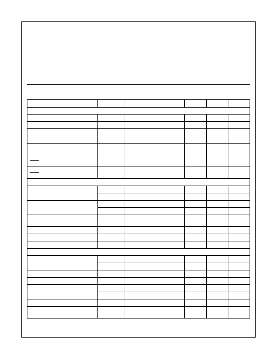
Functional Pin Description
PIN NUMBER
SYMBOL
IN/OUT
DESCRIPTION
1
CLK
Input
This is the clock input that shall be divided by the SBIC (as described in Table 2) and used
as an internal synchronizing clock. The internal clock is then further divided by 128 to de-
termine baud rate, i.e. 128 internal clock periods constitute 1-bit length.
2, 3
A and B
Input
Programing inputs of the clock divider. These inputs are tied to +V
DD
or V
SS
depending
upon speed of external clock source. (See Table 2)
4
Mode
Input
This input shall be used in conjunction with CS input to define the mode of operation (see
Table 1). It may be permanently wired to +V
DD
or V
SS
or driven high or low by MCU I/O
lines.
5, 6
BUS+
and BUS-
Input/Output
This is the two wire differential bus I/O used to transmit and receive data to and from the
differential bus. BUS+ is both responsive to, or driven positive by sourcing current from
an externally established bias point. This sourcing current matches the BUS- I/Os sinking
current. BUS- is both responsive to, or driven negative by sinking current from an exter-
nally established bias point. This sinking current matches the BUS+ I/Os sourcing current.
14, 7
V
DD
and
V
SS
-
Power and ground reference are supplied to the device via these pins. V
DD
is power and
V
SS
is ground.
8
XMIT
Input
In the SCI mode this data input shall come from the microcomputer standard NRZ asyn-
chronous communications output port (68HC05 SCI port pin TxD). In the SPI modes, it
shall come from the microcomputer's synchronous output port (68HC05 SPI port pin
MOSl or MlSO).
9
REC
Output
In the SCI mode this data output shall be fed into the microcomputer asynchronous com-
munications input port (68HC05 SCI port pin RxD). In the SPI modes it shall be fed into
the microcomputer's synchronous input port (6805 SP1 port pin MOSl or MISO).
10
SCK
Input/Output
In the SCI mode, this I/O is not required. In both SPI modes this pin is connected to the
68HC05's SPI port SCK pin. In the normal SPl mode, the SBlC shall produce shift clock
pulses via this pin for synchronously shifting data into and out of the microcomputer. In
the Buffered SPl mode this pin is an input and the microcomputer shall generate the shift
clock pulses. Figure 3 shows the relationship between the serial clock signal and other
SBIC signals in the SPI mode.
11
CS
Input
This input shall be used in conjunction with the mode input and shall be used as a chip
select (see Table 1). It may be permanently wired to +V
DD
or V
SS
or driven high or low by
MCU I/O lines.
12
IDLE
Input/Output
The microcomputer shall monitor this signal to determine the bus condition and also pull
this line low to generate a break. The IDLE signal goes low when the bus is idle (after
sensing an End of Message condition) and high when the bus is active. On reset, this pin
is set to a logic zero.
13
Control
Input/Output
The microcomputer shall monitor this I/O pin in the SPl mode to handle transmission and
reception of data. In the SCI and SPI modes, as an output, this pin will go low to indicate
that a data byte is currently active on the bus. In the Buffered SPI mode the control pin
indicates whether the user microcomputer has current access to the SBI chip's internal 2
byte buffer (signified by a logic high on the control pin). In both SPI modes the control pin
is also effective as an input. In these modes the control pin is pulled low by the user mi-
crocomputer to initiate a transmit operation by the SBlC. The control pin is normally high
when the bus is inactive. On reset, this pin is set to a logic high.