 | –≠–ª–µ–∫—Ç—Ä–æ–Ω–Ω—ã–π –∫–æ–º–ø–æ–Ω–µ–Ω—Ç: DG407/883 | –°–∫–∞—á–∞—Ç—å:  PDF PDF  ZIP ZIP |
1
TM
Features
∑ This Circuit is Processed in Accordance to MIL-STD-883
and is Fully Conformant Under the Provisions of
Paragraph 1.2.1.
∑ ON-Resistance 100
(Max)
∑ Low Power Consumption (P
D
<1.2mW)
∑ Fast Transition Time (300ns Max)
∑ Low Charge Injection
∑ TTL, CMOS Compatible
∑ Single or Split Supply Operation
Applications
∑ Battery Operated Systems
∑ Data Acquisition
∑ Medical Instrumentation
∑ Hi-Rel Systems
∑ Communication Systems
∑ Automatic Test Equipment
Description
The DG406/883 and DG407/883 monolithic CMOS analog
multiplexers are drop-in replacements for the popular
DG506A/883 and DG507A/883 series devices. They each
include an array of sixteen analog switches, a TTL and
CMOS compatible digital decode circuit for channel selec-
tion, a voltage reference for logic thresholds, and an
ENABLE input for device selection when several multiplex-
ers are present.
These multiplexers feature lower signal ON resistance
(<100
) and faster transition time (t
TRANS
<250ns)
compared to the DG506A/883 and DG507A/883. Charge
injection has been reduced, simplifying sample and hold
applications.
The improvements in the DG406 series are made possible by
using a high voltage silicon-gate process. An epitaxial layer
prevents the latch-up associated with older CMOS technolo-
gies. The 44V maximum voltage range permits controlling
30V
P-P
signals when operating with
±15V power supplies.
The sixteen switches are bilateral, equally matched for AC or
bidirectional signals. The ON resistance variation with
analog signals is quite low over a
±5V analog input range.
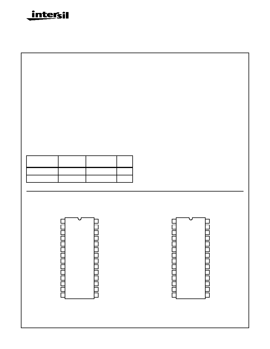
Pinouts
Ordering Information
PART
NUMBER
TEMP. RANGE
(
o
C)
PACKAGE
PKG.
NO.
DG406AK/883
-55 to 125
28 Ld CERDIP
F28.6
DG407AK/883
-55 to 125
28 Ld CERDIP
F28.6
DG406/883
(CERDIP)
TOP VIEW
DG407/883
(CERDIP)
TOP VIEW
V+
NC
NC
S
16
S
15
S
14
S
13
S
12
S
11
S
10
S
9
GND
NC
A
3
D
S
8
S
7
S
6
S
5
S
3
S
1
EN
A
0
A
1
A
2
V-
S
4
S
2
28
27
26
25
24
23
22
21
20
19
18
17
16
15
1
2
3
4
5
6
7
8
9
10
11
12
13
14
V+
D
B
NC
S
8B
S
7B
S
6B
S
5B
S
4B
S
3B
S
2B
S
1B
GND
NC
NC
D
A
S
8A
S
7A
S
6A
S
5A
S
3A
S
1A
EN
A
0
A
1
A
2
V-
S
4A
S
2A
28
27
26
25
24
23
22
21
20
19
18
17
16
15
1
2
3
4
5
6
7
8
9
10
11
12
13
14
April 1997
DG406/883,
DG407/883
Single 16-Channel/Differential
8-Channel CMOS Analog Multiplexers
Spec Number
512041-883
FN3720.1
CAUTION: These devices are sensitive to electrostatic discharge; follow proper IC Handling Procedures.
1-888-INTERSIL or 321-724-7143
|
Intersil (and design) is a trademark of Intersil Americas Inc.
Copyright © Intersil Americas Inc. 2002. All Rights Reserved
2
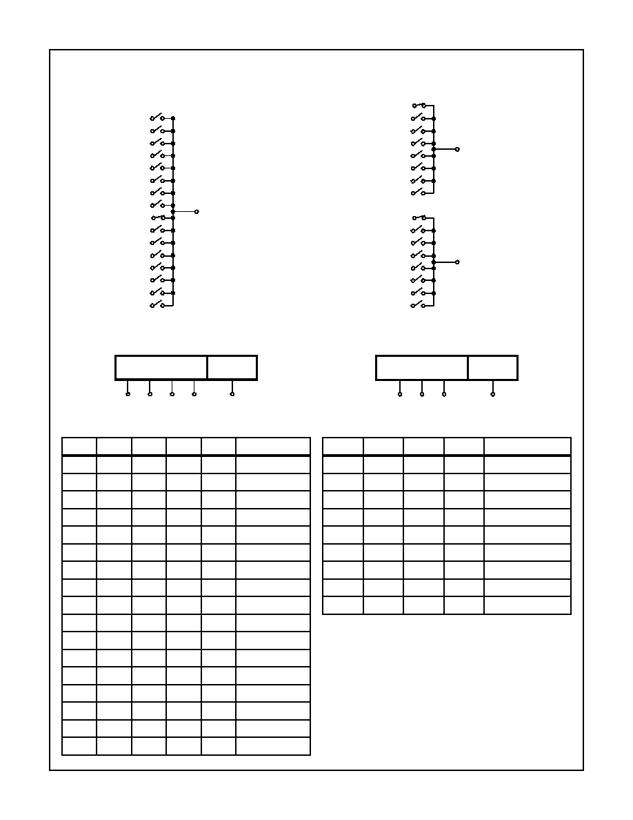
Functional Block Diagrams
DG406
DG407
DG406 TRUTH TABLE
A
3
A
2
A
1
A
0
EN
ON SWITCH
X
X
X
X
0
None
0
0
0
0
1
1
0
0
0
1
1
2
0
0
1
0
1
3
0
0
1
1
1
4
0
1
0
0
1
5
0
1
0
1
1
6
0
1
1
0
1
7
0
1
1
1
1
8
1
0
0
0
1
9
1
0
0
1
1
10
1
0
1
0
1
11
1
0
1
1
1
12
1
1
0
0
1
13
1
1
0
1
1
14
1
1
1
0
1
15
1
1
1
1
1
16
S
1
S
2
S
3
S
4
S
5
S
6
S
7
S
8
S
9
S
10
S
11
S
12
S
13
S
14
S
15
S
16
D
TO DECODER LOGIC
CONTROLLING BOTH
TIERS OF MUXING
ADDRESS DECODER
1 OF 16
ENABLE
A
0
A
1
A
2
A
3
EN
DG407 TRUTH TABLE
A
2
A
1
A
0
EN
ON SWITCH PAIR
X
X
X
0
None
0
0
0
1
1
0
0
1
1
2
0
1
0
1
3
0
1
1
1
4
1
0
0
1
5
1
0
1
1
6
1
1
0
1
7
1
1
1
1
8
Logic "0" = V
AL
< 0.8V
Logic "1" = V
AH
> 2.4V
X = Don't Care
S
2A
S
3A
S
4A
S
5A
S
6A
S
7A
S
8A
S
1B
S
2B
S
3B
S
4B
S
5B
S
6B
S
7B
S
8B
D
A
TO DECODER LOGIC
CONTROLLING BOTH
TIERS OF MUXING
ADDRESS DECODER
1 OF 8
ENABLE
A
0
A
1
A
2
EN
S
1A
D
B
DG406/883, DG407/883
Spec Number
512041-883
3
Absolute Maximum Ratings
Thermal Information
Voltages Referenced to V-
V+ . . . . . . . . . . . . . . . . . . . . . . . . . . . . . . . . . . . . . . . . . . . . +44.0V
GND . . . . . . . . . . . . . . . . . . . . . . . . . . . . . . . . . . . . . . . . . . . . 25V
Digital Inputs, V
S
, V
D
(Note 1) . . . . . . (V-) -2V to (V+) +2V or 20mA,
Whichever Occurs First
Current (Any Terminal) . . . . . . . . . . . . . . . . . . . . . . . . . . . . . . . 30mA
Peak Current, S or D . . . . . . . . . . . . . . . . . . . . . . . . . . . . . . . 100mA
(Pulsed 1ms, 10% Duty Cycle Max)
Operating Conditions
Temperature Range . . . . . . . . . . . . . . . . . . . . . . . . . -55
o
C to 125
o
C
Thermal Resistance (Typical, Note 2)
JA
(
o
C/W)
JC
(
o
C/W)
CERDIP Package . . . . . . . . . . . . . . . .
55
12
Maximum Junction Temperature. . . . . . . . . . . . . . . . . . . . . . . 150
o
C
Maximum Storage Temperature Range . . . . . . . . . . -65
o
C to 150
o
C
CAUTION: Stresses above those listed in "Absolute Maximum Ratings" may cause permanent damage to the device. This is a stress only rating and operation
of the device at these or any other conditions above those indicated in the operational sections of this specification is not implied.
NOTES:
1. Signals on S
X
, D
X
or IN
X
exceeding V+ or V- will be clamped by internal diodes. Limit forward diode current to maximum current ratings.
2.
JA
is measured with the component mounted on an evaluation PC board in free air.
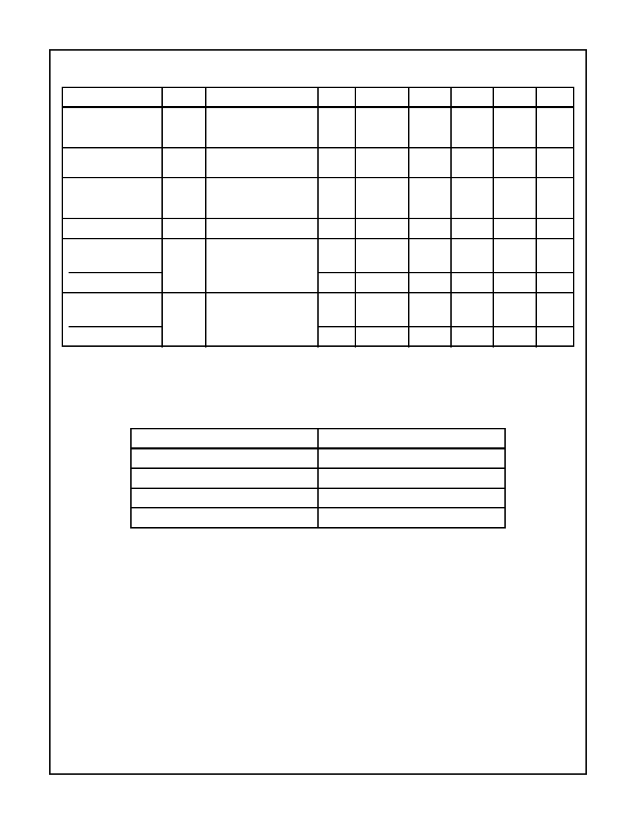
TABLE 1. DC ELECTRICAL PERFORMANCE SPECIFICATIONS
Devices tested at +V
SUPPLY
= +15V, -V
SUPPLY
= -15V, V
AL
= 0.8V, V
AH
= 2.4V, Unless Otherwise Specified
PARAMETER
SYMBOL
CONDITIONS
GROUP A
SUB-
GROUP
DEVICE
TYPE
(NOTE 3)
MIN
(NOTE 3)
MAX
UNITS
Drain-Source ON Resistance
r
DS(ON)
V
D
= 10V, I
S
= -10mA
VD = -10V, IS = 10mA
(Note 4)
1, 3
All
-
90
2
All
-
120
Matching Between Channels
r
DS(ON)
r
DS(ON)
Max - r
DS(ON)
Min
(Note 3)
1
All
-
15
Source OFF Leakage Current
I
S(OFF)
V
EN
= 0V, V
S
=
±10V,
V
D
= +10V
1
All
-0.5
0.5
nA
2, 3
All
-50
50
nA
Drain OFF Leakage Current
I
D(OFF)
V
EN
= 0V, V
S
=
±10V,
V
D
= +10V
DG406
1
DG406
-1
1
nA
2, 3
-200
200
nA
DG407
1
DG407
-1
1
nA
2, 3
-100
100
nA
Drain ON Leakage Current
I
D(ON)
V
S
= V
D
=
±10V
Sequence Each Switch ON
(Note 4)
DG406
1
DG406
-1
1
nA
2, 3
-200
200
nA
DG407
1
DG407
-1
1
nA
2, 3
-100
100
nA
Logic High Input Current
I
AH
V
A
= 2.4V, 15V
1, 2, 3
All
-1
1
µA
Logic Low Input Current
I
AL
V
EN
= 0V, 2.4V, V
A
= 0V
1, 2, 3
All
-1
1
µA
Positive Supply Current
I
CC
V
EN
= 2.4V, V
A
= 0V
1
All
-
100
µA
2, 3
All
-
500
µA
Negative Supply Current
I
EE
1
All
-1
-
µA
2, 3
All
-10
-
µA
DG406/883, DG407/883
Spec Number
512041-883
4
Spec Number
512041-883
Positive Standby Current
I
CC
Standby
V
EN
= V
A
= 0V or 5V
1
All
-
30
µA
2, 3
All
-
75
µA
Negative Standby Current
I
EE
Standby
1
All
-1
-
µA
2, 3
All
-10
-
µA
NOTES:
3. The algebraic convention whereby the most negative value is a minimum and the most positive a maximum, is used in this data sheet.
4. Room = 25
o
C, Cold and Hot = as determined by the operating temperature suffix.
TABLE 1A. ELECTRICAL PERFORMANCE SPECIFICATIONS (SINGLE SUPPLY)
Devices tested at +V
SUPPLY
= +12V, -V
SUPPLY
= 0V, V
AL
= 0.8V, V
AH
= 2.4V, Unless Otherwise Specified
PARAMETER
SYMBOL
CONDITIONS
GROUP A
SUB-
GROUP
DEVICE
TYPE
MIN
MAX
UNITS
Drain-Source ON Resistance
r
DS(ON)
V
D
= 3V, 10V
I
S
= -1mA
1
All
-
120
Positive Current
I
CC
V
EN
= 0V or 5V,
V
A
= 0V or 5V
1
All
-
30
µA
2, 3
All
-
75
µA
Negative Current
I
EE
1
All
-1
-
µA
2, 3
All
-5
-
µA
Switching Time of Multiplexer
t
TRANS
V
S1
= 8V, V
SS
- 0V,
V
IN
= 2.4V
1
All
-
450
ns
Enable Turn-ON Time
t
ON(EN)
V
INH
= 2.4V, V
INL
= 0V,
V
S1
= 5V
1
All
-
600
ns
Enable Turn-OFF Time
t
OFF(EN)
1
All
-
300
ns
TABLE 1. DC ELECTRICAL PERFORMANCE SPECIFICATIONS
Devices tested at +V
SUPPLY
= +15V, -V
SUPPLY
= -15V, V
AL
= 0.8V, V
AH
= 2.4V, Unless Otherwise Specified (Continued)
PARAMETER
SYMBOL
CONDITIONS
GROUP A
SUB-
GROUP
DEVICE
TYPE
(NOTE 3)
MIN
(NOTE 3)
MAX
UNITS
TABLE 2. AC ELECTRICAL PERFORMANCE SPECIFICATIONS
Devices tested at +V
SUPPLY
= +15V, -V
SUPPLY
= -15V, V
AL
= 0.8V, V
AH
= 2.4V, Unless Otherwise Specified
PARAMETER
SYMBOL
CONDITIONS
GROUP A
SUB-
GROUP
DEVICE
TYPE
MIN
MAX
UNITS
Transition Time
t
TRANS
C
L
= 35pF, R
L
= 300
,
See Figure 1
9
All
-
300
ns
10, 11
All
-
400
ns
Enable Turn-ON Time
t
ON(EN)
C
L
= 35pF, R
L
= 300
,
See Figure 2
9
All
-
200
ns
10, 11
All
-
400
ns
Enable Turn-OFF Time
t
OFF(EN)
9
All
-
150
ns
10, 11
All
-
300
ns
Break Before Leakage Current
t
OPEN
C
L
= 35pF, R
L
= 300
,
See Figure 3
9
All
25
-
ns
10, 11
All
10
-
ns
DG406/883, DG407/883
5
TABLE 3. DC ELECTRICAL PERFORMANCE SPECIFICATIONS
Devices tested at +V
SUPPLY
= +15V, -V
SUPPLY
= -15V, V
AL
= 0.8V, V
AH
= 2.4V, Unless Otherwise Specified
PARAMETER
SYMBOL
CONDITIONS
NOTE
TEMP (
o
C)
MIN
TYP
MAX
UNITS
Off Isolation Time
V
ISO
V
EN
= 0V, R
L
= 1K,
f = 100kHz, GEN = 1V
P-P
Sine Wave, See Figure 5
5
25
50
-
-
dB
Charge Transfer Error
V
CTE
C
L
= 10nF, V
S
= 0V, R
S
= 0
,
See Figure 4
5
25
-
-
10
mV
Crosstalk
V
CT
R
L
= 1K, f = 100kHz,
GEN = 1V
P-P
Sine Wave, See
Figure 5
5
25
50
-
-
dB
Source OFF Capacitance
C
S(OFF)
V
EN
= 0V, V
S
= 0V, f = 1MHz
65
25
-
-
10
pF
Drain OFF Capacitance
C
D(OFF)
V
EN
= 0V, V
D
= 0V, f = 1MHz
DG406
5
25
-
-
200
pF
DG407
5
25
-
-
100
pF
Drain ON Capacitance
C
D(ON)
V
EN
= 0V, V
D
= 0V, f = 1MHz
DG406
5
25
-
-
400
pF
DG407
5
25
-
-
200
pF
NOTE:
5. Parameters listed via process parameters and are not directly tested at final production. These parameters are lab characterized upon
design release, or upon design changes. These parameters are guaranteed by characterization based upon data from multiple produc-
tion rich reflect lot to lot and within lot variation.
TABLE 4. ELECTRICAL TEST REQUIREMENTS
MIL-STD-883 TEST REQUIREMENTS
SUBGROUPS (SEE TABLES 1 AND 2)
Interim Electrical Parameters (Pre Burn0In)
1
Final Electrical Test Parameters
1 (Note 6), 2, 3, 9, 10, 11
Group A Test Requirements
1, 2, 3, 9, 10, 11
Group C and D Endpoints
1
NOTE:
6. PDA applied to Subgroup 1 only.
DG406/883, DG407/883
Spec Number
512041-883
6
Spec Number
512041-883
Test Circuits and Waveforms
FIGURE 1A.
FIGURE 1B.
FIGURE 1C.
FIGURE 1. TRANSITION TIME
FIGURE 2A.
FIGURE 2B.
FIGURE 2C.
EN
A3
DG406
GND
A
2
A
1
S
1
S
2
- S
15
S
16
D
V-
V+
±
±10V
V
O
35pF
300
50
+15V
+2.4V
-
15V
A
0
10V
EN
A
0
DG407
GND
A
1
A
2
S
1B
S
8B
D
B
V-
V+
±10V
V
O
35pF
300
50
+15V
+2.4V
-
15V
= S
1A
- S
8A
, S
2B
- S
7B
, D
A
±
10V
LOGIC
INPUT
SWITCH
OUTPUT
V
O
3V
V
S1B
50%
t
r
< 20ns
t
f
< 20ns
t
TRANS
50%
0V
0V
V
S8B
t
TRANS
S
8
ON
80%
80%
S
1
ON
EN
A3
DG406
GND
A
2
A
1
S
1
S
2
- S
16
D
V-
V+
-5V
V
O
35pF
300
50
+15V
-
15V
A
0
EN
A
0
DG407
GND
A
1
A
2
S
1B
D
B
V-
V+
-5V
V
O
35pF
300
50
+15V
-
15V
= S
1A
- S
8A
, S
2B
- S
8B
, D
A
LOGIC
INPUT
SWITCH
OUTPUT
V
O
3V
V
O
50%
t
r
< 20ns
t
f
< 20ns
t
ON(EN)
0V
50%
t
OFF(EN)
90%
0V
DG406/883, DG407/883
7
FIGURE 2. ENABLE SWITCHING TIME
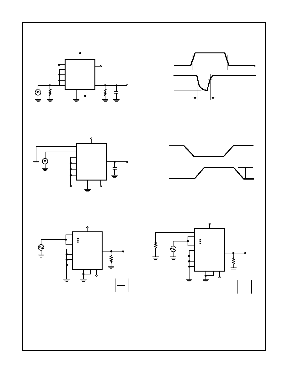
FIGURE 3A.
FIGURE 3B.
FIGURE 3. BREAK-BEFORE-MAKE INTERVAL
FIGURE 4. CHARGE INJECTION
FIGURE 5. OFF ISOLATION
FIGURE 6. CROSSTALK
Test Circuits and Waveforms
(Continued)
EN
A3
DG406
GND
A
2
A
1
ALL S
D,
V-
V+
+5V
V
O
35pF
300
50
+15V
+2.4V
-
15V
A
0
DG407
AND D
A
D
B
LOGIC
INPUT
SWITCH
OUTPUT
V
O
3V
V
D
t
r
< 20ns
t
f
< 20ns
t
OPEN
0V
0V
80%
50%
S
X
A
0
DG406
GND
A
1
A
2
D
V-
V+
V
O
C
L
+15V
-
15V
A
3
DG407
EN
V
GEN
= 0-3V
10nF
5V
V
O
OFF
OFF
ON
3V
0V
LOGIC
INPUT
SWITCH
OUTPUT
S
X1
A
0
DG406
GND
A
1
A
2
D
V-
V+
V
O
R
L
R
G
= 50
+15V
-
15V
A
3
DG407
S
X16
V
GEN
= 1V
P-P
1k
OFF ISOLATION = 20LOG
V
OUT
V
IN
EN
V
S
A
0
DG406
GND
A
1
A
2
D
V-
V+
V
O
R
L
R
G
= 50
+15V
-
15V
A
3
DG407
1V
P-P
1k
EN
S
1
1k
V
S
CROSSTALK = 20LOG
V
OUT
V
IN
S
X2
S
X16
DG406/883, DG407/883
Spec Number
512041-883
8
Spec Number
512041-883
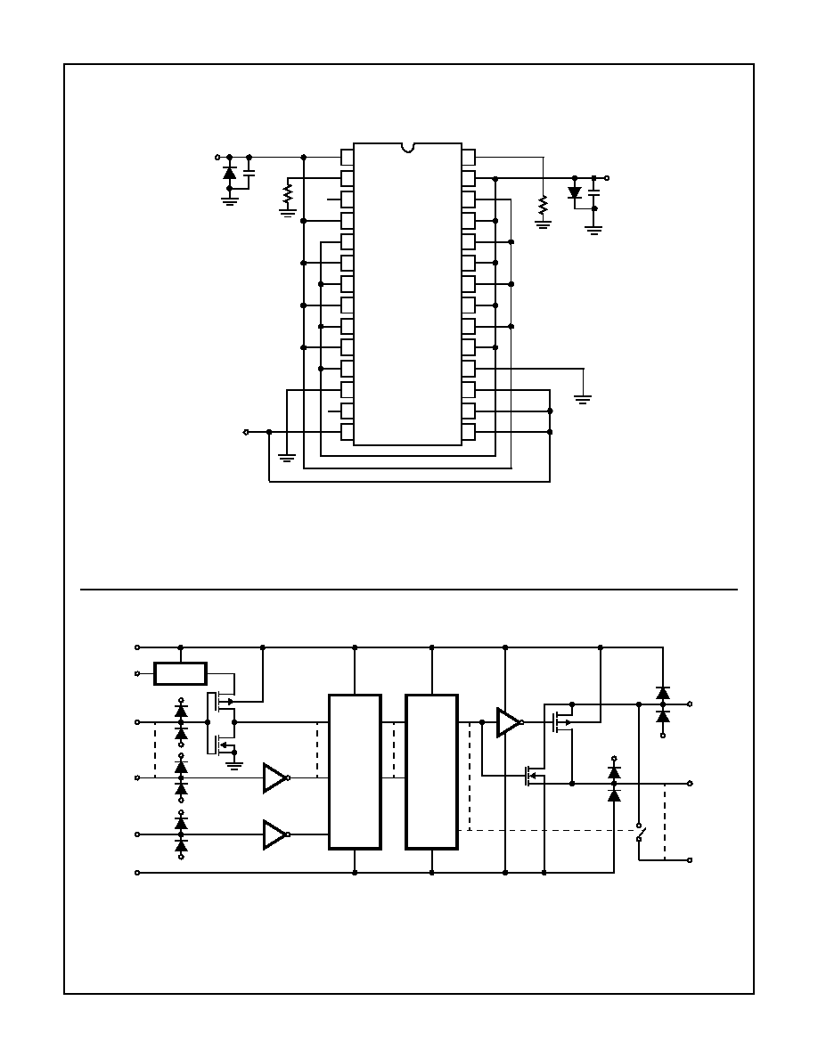
Burn-In Circuit
CERDIP BURN-IN SCHEMATIC
DG406/407AK/883
NOTE:
R
1
, R
2
= 10k
±5%, 1/2W or 1/4W (Per Socket)
C
1
, C
2
= 0.01
µF (Min, Per Socket) or 0.1µF (Min, Per Row)
D
1
, D
2
= IN402 (or Equivalent, Per Board)
Schematic Diagram
(Typical Channel)
+15V
D
1
C
1
R
1
28
27
26
25
24
23
22
21
20
19
18
17
16
15
1
2
3
4
5
6
7
8
9
10
11
12
13
14
OUT/OUTA
-V
IN 8/8A
IN 7/7A
IN 6/6A
IN 5/5A
IN 4/4A
IN 3/3A
IN 2/2A
IN 1/1A
EN
A0
A1
A2
A3/NC
VREF
GND
IN 9/1B
IN 10/2B
IN 11/3B
IN 12/4B
IN 13/5B
IN 14/6B
IN 15/7B
IN 16/8B
NC
NC/OUT B
+V
R
2
-15V
D
2
C
2
+5V
V+
GND
A
0
A
X
EN
V-
V
REF
LEVEL
SHIFT
DECODE/
DRIVE
V+
V+
V-
D
S
1
S
N
DG406/883, DG407/883
9
Typical Design Information
The information contained in this section has been developed through characterization by Harris Semiconductor and is for use as applica-
tion and design information only. No guarantee is implied.
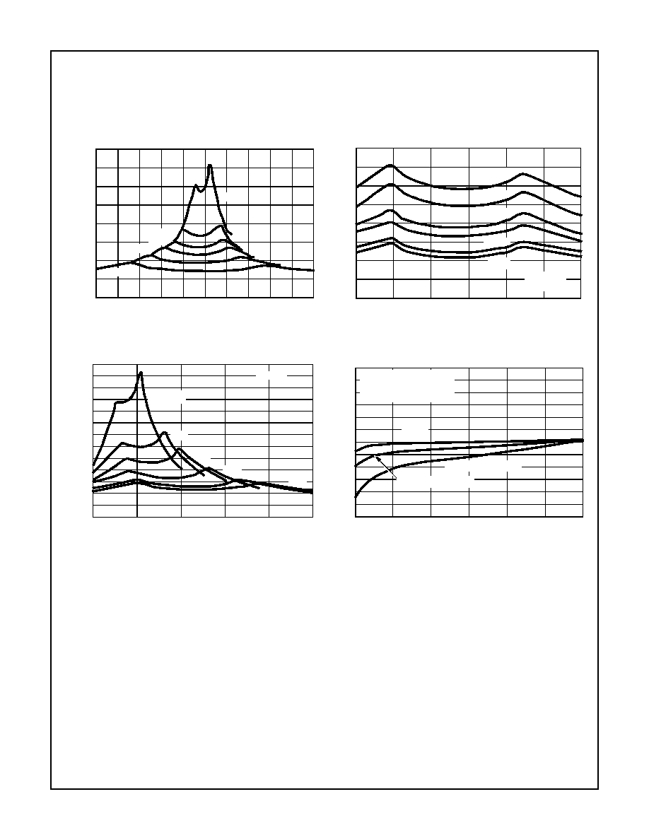
Typical Performance Curves
FIGURE 7. r
DS(ON)
vs V
D
AND SUPPLY
FIGURE 8. r
DS(ON)
vs V
D
AND TEMPERATURE
FIGURE 9. r
DS(ON)
vs V
D
AND SUPPLY
FIGURE 10. I
D
, I
S
LEAKAGE CURRENTS vs ANALOG VOLT-
AGE
±5V
±8V
±10V
±12V
±15V
±20V
160
140
120
100
80
60
40
20
0
-20
-16
-12
-8
-4
0
4
8
12
16
20
V
D
, DRAIN VOLTAGE (V)
r
DS
(O
N)
,
O
N
RE
S
I
S
T
ANCE
(
)
125
o
C
-40
o
C
-55
o
C
25
o
C
85
o
C
0
o
C
V+ = 15V
V- = -15V
80
70
60
50
40
30
20
10
0
-15
-10
-5
5
10
0
15
V
D
, DRAIN VOLTAGE (V)
r
DS
(
O
N
)
, O
N
-
R
E
S
IS
T
ANCE
(
)
V- = 0V
V+ = 7.5V
10V
12V
15V
20V
22V
240
200
160
120
80
40
0
0
4
8
12
16
20
V
D
, DRAIN VOLTAGE (V)
r
DS
(O
N)
, O
N
-
R
E
S
IS
T
ANCE
(
)
-10
-5
5
10
0
15
V
S
, V
D
, SOURCE DRAIN VOLTAGE (V)
V+ = 15V, V- = -15V
V
S
= -V
D
FOR I
D(OFF)
V
D
= V
S(OPEN)
FOR I
D(ON)
I
S(OFF)
DG406 I
D(ON)
, I
D(OFF)
-15
120
80
40
0
-40
-80
-120
I
D
, I
S
, CURR
E
N
T
(
p
A)
DG407 I
D(ON)
, I
D(OFF)
DG406/883, DG407/883
Spec Number
512041-883
10
Spec Number
512041-883
FIGURE 11. I
D
, I
S
LEAKAGE vs TEMPERATURE
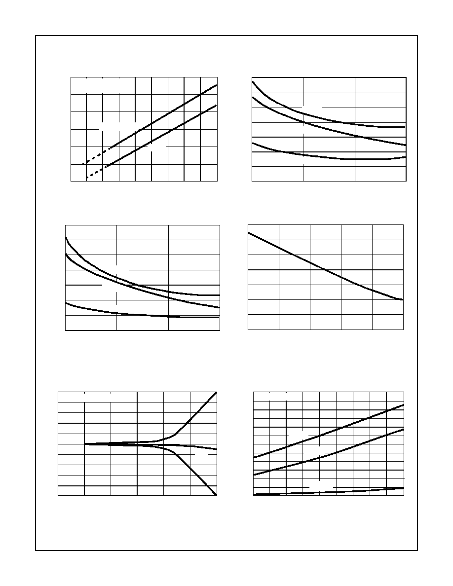
FIGURE 12. SWITCHING TIMES vs BIPOLAR SUPPLIES
FIGURE 13. SWITCHING TIMES vs SINGLE SUPPLY
FIGURE 14. OFF-ISOLATION vs FREQUENCY
FIGURE 15. SUPPLY CURRENTS vs SWITCHING FREQUENCY
FIGURE 16. t
ON
/t
OFF
vs TEMPERATURE
Typical Performance Curves
(Continued)
V+ = 15V, V- = -15V
V
S
OR V
D
=
±10V
I
S(OFF)
I
D(ON)
, I
D(OFF)
100nA
10nA
1nA
100pA
10pA
1pA
0.1pA
I
D
, I
S
, CURRE
NT
(
A
)
-55
-35
-15
5
25
45
65
85
105
125
TEMPERATURE (
o
C)
350
300
250
200
150
100
50
0
5
10
15
20
V
SUPPLY
, SUPPLY VOLTAGE (
±V)
TI
M
E
(
n
s
)
t
TRANS
t
ON(EN)
t
OFF(EN)
700
600
500
400
300
200
100
0
5
10
15
20
V+, SUPPLY VOLTAGE (V)
TI
M
E
(ns
)
t
TRANS
t
ON(EN)
t
OFF(EN)
V- = 0V
1K
10K
1M
100K
10M
f, FREQUENCY (Hz)
100
-140
-120
-100
-80
-60
-40
-20
IS
O
L
(
d
B
)
0
100
1K
100K
1M
10K
10M
f, FREQUENCY (Hz)
E
N
= 5V, A
X
= 0V OR 5V
I
GND
10
10
8
6
0
-4
-8
-10
I
,
CURRE
NT
(
m
A)
I+
I-
4
2
-2
-6
300
280
260
240
220
200
140
120
60
-55
-35
-15
5
25
45
65
85
105
125
TEMPERATURE (
o
C)
TI
M
E
(ns
)
180
160
100
80
t
TRANS
t
ON(EN)
t
OFF(EN)
V+ = 15V, V- = -15V
DG406/883, DG407/883
11
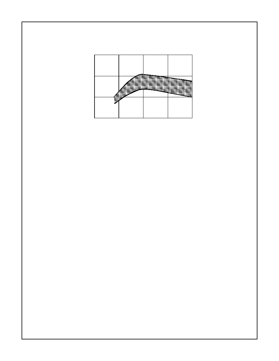
FIGURE 17. SWITCHING THRESHOLD vs SUPPLY VOLTAGE
Typical Performance Curves
(Continued)
5
10
15
20
V
SUPPLY
, SUPPLY VOLTAGE (
±V)
0
0
1
2
3
V
A
(V
)
DG406/883, DG407/883
Spec Number
512041-883
12
Spec Number
512041-883
Die Characteristics
DIE DIMENSIONS:
2490
µm x 4560µm x 485µm ±25µm
METALLIZATION:
Type: SiAl
Thickness: 12k
≈
±1k
≈
PASSIVATION:
Type: Nitride
Thickness: 8k
≈
±1k
≈
WORST CASE CURRENT DENSITY:
9.1 x 10
4
A/cm
2
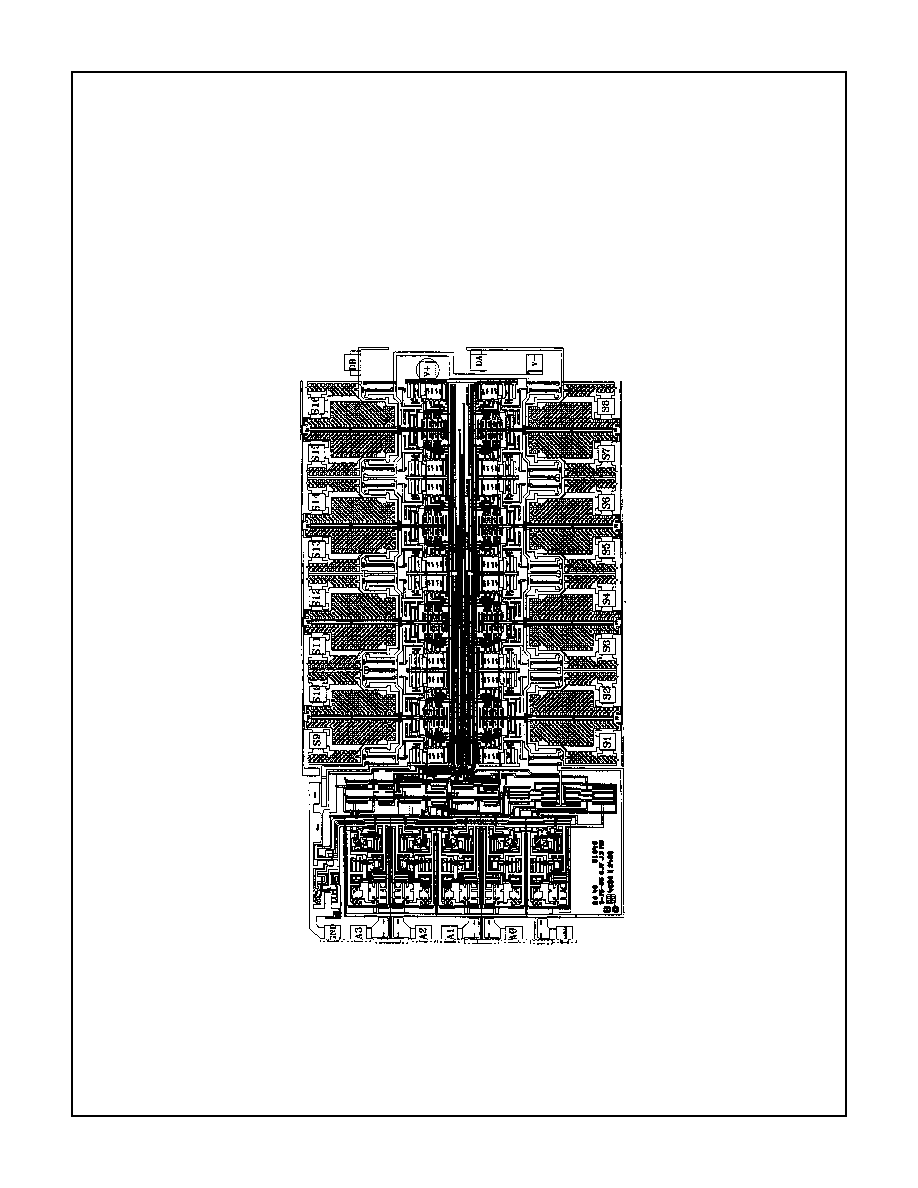
Metallization Mask Layout
DG406/883
Die Characteristics
DIE DIMENSIONS:
2490
µm x 4560µm x 485µm ±25µm
V-
S
16
D
NC
V+
S
8
A
0
EN
S
7
S
6
S
5
S
4
S
3
S
2
S
1
A
1
A
2
A
3
GND
S
15
S
14
S
13
S
12
S
11
S
10
S
9
DG406/883, DG407/883
13
All Intersil U.S. products are manufactured, assembled and tested utilizing ISO9000 quality systems.
Intersil Corporation's quality certifications can be viewed at www.intersil.com/design/quality
Intersil products are sold by description only. Intersil Corporation reserves the right to make changes in circuit design, software and/or specifications at any time without
notice. Accordingly, the reader is cautioned to verify that data sheets are current before placing orders. Information furnished by Intersil is believed to be accurate and
reliable. However, no responsibility is assumed by Intersil or its subsidiaries for its use; nor for any infringements of patents or other rights of third parties which may result
from its use. No license is granted by implication or otherwise under any patent or patent rights of Intersil or its subsidiaries.
For information regarding Intersil Corporation and its products, see www.intersil.com
Sales Office Headquarters
NORTH AMERICA
Intersil Corporation
7585 Irvine Center Drive
Suite 100
Irvine, CA 92618
TEL: (949) 341-7000
FAX: (949) 341-7123
Intersil Corporation
2401 Palm Bay Rd.
Palm Bay, FL 32905
TEL: (321) 724-7000
FAX: (321) 724-7946
EUROPE
Intersil Europe Sarl
Ave. William Graisse, 3
1006 Lausanne
Switzerland
TEL: +41 21 6140560
FAX: +41 21 6140579
ASIA
Intersil Corporation
Unit 1804 18/F Guangdong Water Building
83 Austin Road
TST, Kowloon Hong Kong
TEL: +852 2723 6339
FAX: +852 2730 1433
DG406/883, DG407/883
Spec Number
512041-883
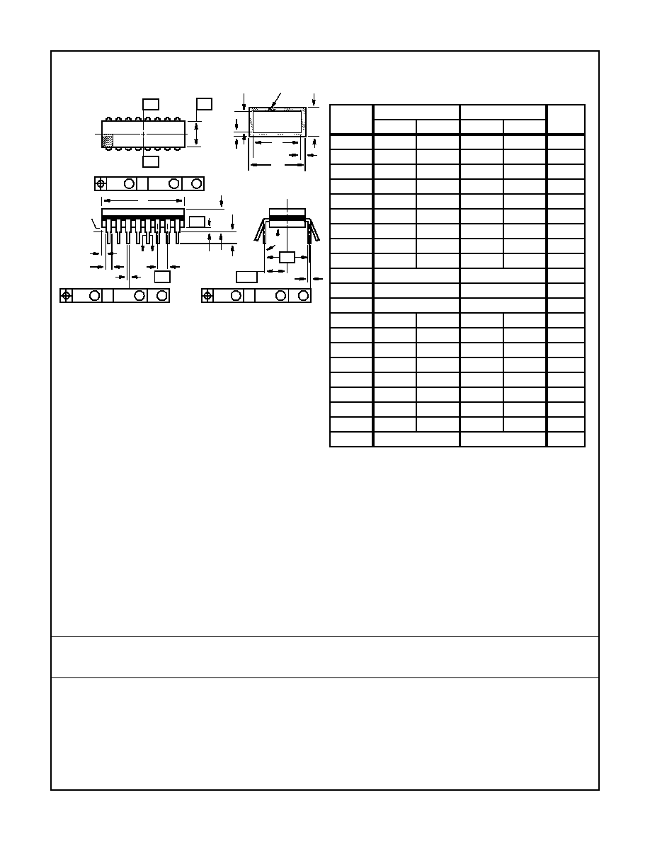
NOTES:
1. Index area: A notch or a pin one identification mark shall be lo-
cated adjacent to pin one and shall be located within the shaded
area shown. The manufacturer's identification shall not be used
as a pin one identification mark.
2. The maximum limits of lead dimensions b and c or M shall be
measured at the centroid of the finished lead surfaces, when
solder dip or tin plate lead finish is applied.
3. Dimensions b1 and c1 apply to lead base metal only. Dimension
M applies to lead plating and finish thickness.
4. Corner leads (1, N, N/2, and N/2+1) may be configured with a
partial lead paddle. For this configuration dimension b3 replaces
dimension b2.
5. This dimension allows for off-center lid, meniscus, and glass
overrun.
6. Dimension Q shall be measured from the seating plane to the
base plane.
7. Measure dimension S1 at all four corners.
8. N is the maximum number of terminal positions.
9. Dimensioning and tolerancing per ANSI Y14.5M - 1982.
10. Controlling dimension: INCH.
bbb
C A - B
S
c
Q
L
A
SEATING
BASE
D
PLANE
PLANE
-D-
-A-
-C-
-B-
D
E
S1
b2
b
A
e
M
c1
b1
(c)
(b)
SECTION A-A
BASE
LEAD FINISH
METAL
e
A/2
A
M
S
S
ccc
C A - B
M
D
S
S
aaa
C A - B
M
D
S
S
e
A
Ceramic Dual-In-Line Frit Seal Packages (CERDIP)
F28.6
MIL-STD-1835 GDIP1-T28 (D-10, CONFIGURATION A)
28 LEAD CERAMIC DUAL-IN-LINE FRIT SEAL PACKAGE
SYMBOL
INCHES
MILLIMETERS
NOTES
MIN
MAX
MIN
MAX
A
-
0.232
-
5.92
-
b
0.014
0.026
0.36
0.66
2
b1
0.014
0.023
0.36
0.58
3
b2
0.045
0.065
1.14
1.65
-
b3
0.023
0.045
0.58
1.14
4
c
0.008
0.018
0.20
0.46
2
c1
0.008
0.015
0.20
0.38
3
D
-
1.490
-
37.85
5
E
0.500
0.610
12.70
15.49
5
e
0.100 BSC
2.54 BSC
-
eA
0.600 BSC
15.24 BSC
-
eA/2
0.300 BSC
7.62 BSC
-
L
0.125
0.200
3.18
5.08
-
Q
0.015
0.060
0.38
1.52
6
S1
0.005
-
0.13
-
7
90
o
105
o
90
o
105
o
-
aaa
-
0.015
-
0.38
-
bbb
-
0.030
-
0.76
-
ccc
-
0.010
-
0.25
-
M
-
0.0015
-
0.038
2, 3
N
28
28
8
Rev. 0 4/94