 | –≠–ª–µ–∫—Ç—Ä–æ–Ω–Ω—ã–π –∫–æ–º–ø–æ–Ω–µ–Ω—Ç: DG409/883 | –°–∫–∞—á–∞—Ç—å:  PDF PDF  ZIP ZIP |

5-34
DG408/883,
DG409/883
Single 8-Channel/Differential
4-Channel CMOS Analog Multiplexers
Description
The DG408/883 Single 8-Channel and DG409/883 Differen-
tial 4-Channel monolithic CMOS analog multiplexers are
drop-in replacements for the popular DG508A and DG509A
series devices. They each include an array of eight analog
switches, a TTL/CMOS compatible digital decode circuit for
channel selection, a voltage reference for logic thresholds
and an ENABLE input for device selection when several mul-
tiplexers are present.
The DG408/883 and DG409/883 feature lower signal ON
resistance (<100
) and faster switch transition time (t
TRANS
<250ns) compared to the DG508A or DG509A. Charge
injection has been reduced, simplifying sample and hold
applications. The improvements in the DG408/883 series are
made possible by using a high-voltage silicon-gate process.
An epitaxial layer prevents the latch-up associated with older
CMOS technologies. Power supplies may be single-ended
from +5V to +34V, or split from
±
5V to
±
20V.
The analog switches are bilateral, equally matched for AC or
bidirectional signals. The ON resistance variation with ana-
log signals is quite low over a
±
5V analog input range.
Ordering Information
PART
NUMBER
TEMPERATURE
RANGE
PACKAGE
DG408AK/883
-55
o
C to +125
o
C
16 Lead CerDIP
DG409AK/883
-55
o
C to +125
o
C
16 Lead CerDIP
Features
∑ This Circuit is Processed in Accordance to MIL-STD-
883 and is Fully Conformant Under the Provisions of
Paragraph 1.2.1.
∑ ON-Resistance 100
Maximum (+25
o
C)
∑ Low Power Consumption (P
D
<11mW)
∑ Fast Switching Action
- t
TRANS
<250ns
- t
ON/OFF(EN)
<150ns
∑ Low Charge Injection
∑ Upgrade from DG508A/DG509A
∑ TTL, CMOS Compatible
∑ Single or Split Supply Operation
Applications
∑ Data Acquisition Systems
∑ Audio Switching Systems
∑ Automatic Testers
∑ Hi-Rel Systems
∑ Sample and Hold Circuits
∑ Communication Systems
∑ Analog Selector Switch
June 1994
Pinouts
DG408/883
(CERDIP)
TOP VIEW
DG409/883
(CERDIP)
TOP VIEW
14
15
16
9
13
12
11
10
1
2
3
4
5
7
6
8
A
0
EN
V-
S
1
S
2
S
3
D
S
4
A
1
GND
V+
S
5
S
6
S
7
S
8
A
2
14
15
16
9
13
12
11
10
1
2
3
4
5
7
6
8
A
0
EN
V-
S
1A
S
2A
S
3A
D
A
S
4A
A
1
V+
S
1B
S
3B
S
4B
D
B
GND
S
2B
Spec Number
512045
File Number
3688

5-35
DG408/883, DG409/883
Functional Block Diagrams
DG408/883
DG409/883
DECODER/
DRIVER
D
LEVEL
SHIFT
*
*
*
*
5V
REF
DIGITAL
INPUT
PROTECTION
*
S
1
S
2
S
8
A
0
A
1
A
2
EN
DECODER/
DRIVER
D
A
LEVEL
SHIFT
*
*
*
5V
REF
DIGITAL
INPUT
PROTECTION
*
S
1A
S
4A
S
1B
A
0
A
1
EN
D
B
S
4B
Spec Number
512045

5-36
DG408/883, DG409/883
Pin Description
- (DG408/883)
PIN
SYMBOL
DESCRIPTION
1
A
0
Logic Decode Input (Bit 0, LSB)
2
EN
Enable Input
3
V-
Negative Power Supply Terminal
4
S
1
Source (Input) for Channel 1
5
S
2
Source (Input) for Channel 2
6
S
3
Source (Input) for Channel 3
7
S
4
Source (Input) for Channel 4
8
D
Drain (Output)
9
S
8
Source (Input) for Channel 8
10
S
7
Source (Input) for Channel 7
11
S
6
Source (Input) for Channel 6
12
S
5
Source (Input) for Channel 5
13
V+
Positive Power Supply Terminal (Substrate)
14
GND
Ground Terminal (Logic Common)
15
A
2
Logic Decode Input (Bit 2, MSB)
16
A
1
Logic Decode Input (Bit 1)
TRUTH TABLE DG408/883
A
2
A
1
A
0
EN
ON SWITCH
X
X
X
0
NONE
0
0
0
1
1
0
0
1
1
2
0
1
0
1
3
0
1
1
1
4
1
0
0
1
5
1
0
1
1
6
1
1
0
1
7
1
1
1
1
8
Pin Description
- (DG409/883)
PIN
SYMBOL
DESCRIPTION
1
A
0
Logic Decode Input (Bit 0, LSB)
2
EN
Enable Input
3
V-
NegAtive Power Supply Terminal
4
S
1A
Source (Input) for Channel 1A
5
S
2A
Source (Input) for Channel 2A
6
S
3A
Source (Input) for Channel 3A
7
S
4A
Source (Input) for Channel 4A
8
D
A
Drain A (Output A)
9
D
B
Drain B (Output B)
10
S
4B
Source (Input) for Channel 4B
11
S
3B
Source (Input) for Channel 3B
12
S
2B
Source (Input) for Channel 2B
13
S
1B
Source (Input) for Channel 1B
14
V+
Positive Power Supply Terminal
15
GND
Ground Terminal (Logic Common)
16
A
1
Logic Decode Input (Bit 1, MSB))
TRUTH TABLE DG409/883
A
1
A
0
EN
ON SWITCH
X
X
0
NONE
0
0
1
1
0
1
1
2
1
0
1
3
1
1
1
4
NOTES:
1. V
AH
Logic "1"
2.4V.
2. V
AL
Logic "0"
0.8V.
Spec Number
512045

5-37
Specifications DG408/883, DG409/883
Absolute Maximum Ratings
Thermal Information
V+ to V-. . . . . . . . . . . . . . . . . . . . . . . . . . . . . . . . . . . . . . . . . . +44.0V
GND to V- . . . . . . . . . . . . . . . . . . . . . . . . . . . . . . . . . . . . . . . . . . 25V
Digital Inputs (Note 1). . . . . . . . . . . . (V-) -2V to (V+) + 2V or 20mA,
Whichever Occurs First
Current (Any Terminal, Except S or D) . . . . . . . . . . . . . . . . . . . 30mA
Continuous Current, S or D . . . . . . . . . . . . . . . . . . . . . . . . . . . 20mA
Peak Current, S or D . . . . . . . . . . . . . . . . . . . . . . . . . . . . . . . . 40mA
(Pulsed 1ms, 10% Duty Cycle)
Storage Temperature Range . . . . . . . . . . . . . . . . . -65
o
C to +125
o
C
Lead Temperature (Soldering, 10s) . . . . . . . . . . . . . . . . . . . +300
o
C
Thermal Resistance
JA
JC
CerDIP Package . . . . . . . . . . . . . . . . . . .
70
o
C/W
20
o
C/W
Operating Temperature . . . . . . . . . . . . . . . . . . . . . . -55
o
C to +125
o
C
Junction Temperature . . . . . . . . . . . . . . . . . . . . . . . . . . . . . . +175
o
C
CAUTION: Stresses above those listed in "Absolute Maximum Ratings" may cause permanent damage to the device. This is a stress only rating and operation
of the device at these or any other conditions above those indicated in the operational sections of this specification is not implied.
TABLE 1. DC ELECTRICAL PERFORMANCE CHARACTERISTICS
Device Tested at: -55
o
C
T
A
+125
o
C, V+ = +15V, V- = -15V, Unless Otherwise Specified
PARAMETERS
SYMBOL
CONDITIONS
GROUP A
SUBGROUP
TEMPERATURE
LIMITS
UNITS
MIN
MAX
Drain-Source ON
Resistance
r
DS(ON)
V
D
=
±
10V, V
AL
= 0.8V,
V
AH
= 2.4V, I
S
= -10mA,
Sequence Each Switch On
1, 3
+25
o
C, -55
o
C
-
100
2
+125
o
C
-
125
Difference In Drain-
Source ON Resistance
Between Channels
r
DS(ON)
V
D
=
±
10V, V
AL
= 0.8V,
V
AH
= 2.4V, I
S
= -10mA,
(Note 2)
1
+25
o
C
-
15
Source OFF Leakage
Current
I
S(OFF)
V
S
=
±
10V, V
D
=
10V,
V
EN
= 0V
1
+25
o
C
-0.5
+0.5
nA
2
+125
o
C
-50
+50
nA
Drain OFF Leakage
Current
I
D(OFF)
V
S
=
±
10V, V
D
=
10V,
V
EN
= 0V
1
+25
o
C
-1
+1
nA
DG408/883
2
+125
o
C
-200
+200
nA
DG409/883
1
+25
o
C
-1
+1
nA
2
+125
o
C
-100
+100
nA
Drain ON Leakage
Current
I
D(ON)
V
S
= V
D
=
±
10V,
V
AL
= 0.8V, V
AH
= 2.4V,
V
EN
= 2.4V,
Sequence Each Switch On
1
+25
o
C
-1
+1
nA
DG408/883
2
+125
o
C
-200
+200
nA
DG409/883
1
+25
o
C
-1
+1
nA
2
+125
o
C
-150
+150
nA
Logic Input Current,
Input Voltage High
I
AH
V
EN
= 0.8V, V
A
= 2.4V
1, 2, 3
+25
o
C, +125
o
C,
-55
o
C
-10
+10
µ
A
V
EN
= 0.8V, V
A
= 15V
-10
+10
µ
A
Logic Input Current,
Input Voltage Low
I
AL
V
EN
= 0V, V
A
= 0V
1, 2, 3
+25
o
C, +125
o
C,
-55
o
C
-10
+10
µ
A
V
EN
= 2.4V, V
A
= 0V
-10
+10
µ
A
Positive Supply
Current Standby
I+
(SB)
V
EN
= 0V, V
A
= 0V
1, 2, 3
+25
o
C, +125
o
C,
-55
o
C
-
75
µ
A
±
±
Spec Number
512045
5-38
Specifications DG408/883, DG409/883
Negative Supply
Current Standby
I-
(SB)
V
EN
= 0V, V
A
= 0V
1, 2, 3
+25
o
C, +125
o
C,
-55
o
C
-75
-
µ
A
Positive Supply
Current
I+
V
EN
= 2.4V, V
A
= 0V
1, 3
+25
o
C, -55
o
C
-
0.5
mA
2
+125
o
C
-
2
mA
Negative Supply
Current
I-
V
EN
= 2.4V, V
A
= 0V
1, 2, 3
+25
o
C, +125
o
C,
-55
o
C
-0.5
-
mA
TABLE 2. AC ELECTRICAL PERFORMANCE CHARACTERISTICS
Device Tested at: -55
o
C
T
A
+125
o
C, V+ = +15V, V- = -15V, Unless Otherwise Specified
PARAMETERS
SYMBOL
CONDITIONS
GROUP A
SUBGROUP
TEMPERATURE
LIMITS
UNITS
MIN
MAX
Switching Time of
Multiplexer
t
TRANS
9, 10, 11
+25
o
C, +125
o
C,
-55
o
C
-
250
ns
Enable Turn ON Time
t
ON(EN)
9, 11
+25
o
C, -55
o
C
-
150
ns
10
+125
o
C
-
225
ns
Enable Turn OFF Time
t
OFF(EN)
9, 10, 11
+25
o
C, +125
o
C,
-55
o
C
-
150
ns
Break-Before-Make
Interval
t
OPEN
9
+25
o
C
10
-
ns
TABLE 3. ELECTRICAL PERFORMANCE CHARACTERISTICS
Table 3 Intentionally Left Blank.
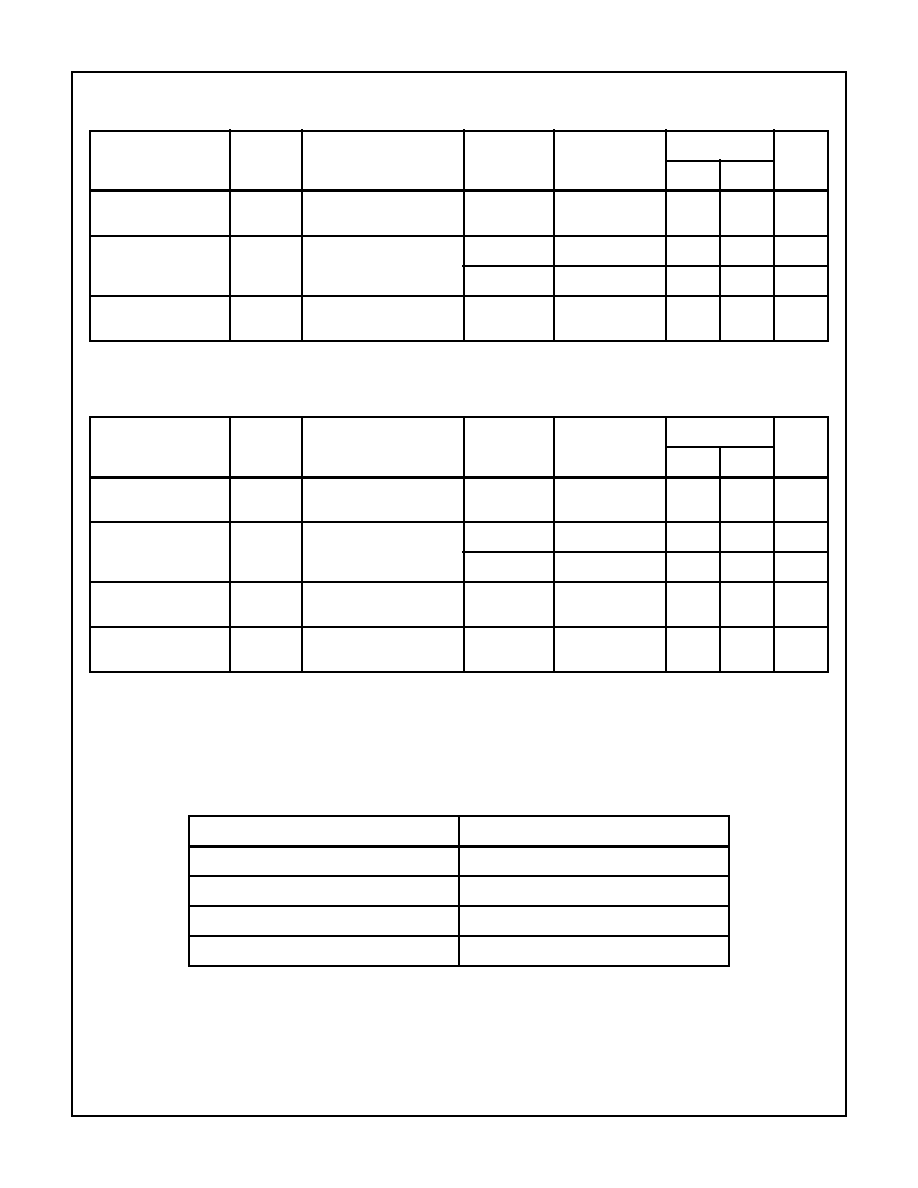
TABLE 4. ELECTRICAL TEST REQUIREMENTS
MIL-STD-883 TEST REQUIREMENTS
SUBGROUPS (SEE TABLES 1 AND 2)
Interim Electrical Parameters (Pre Burn-In)
1
Final Electrical Test Parameters
1 (Note 3), 2, 3, 9, 10, 11
Group A Test Requirements
1, 2, 3, 9, 10, 11
Groups C and D Endpoints
1
NOTES:
1. Signals on S
X
, D
X
, or IN
X
exceeding V+ or V- will be clamped by internal diodes. Limit forward diode
current to maximum current ratings.
2.
r
DS(ON)
= r
DS(ON)
MAX - r
DS(ON)
MIN.
3. PDA applies to Subgroup 1 only.
TABLE 1. DC ELECTRICAL PERFORMANCE CHARACTERISTICS
(Continued)
Device Tested at: -55
o
C
T
A
+125
o
C, V+ = +15V, V- = -15V, Unless Otherwise Specified
PARAMETERS
SYMBOL
CONDITIONS
GROUP A
SUBGROUP
TEMPERATURE
LIMITS
UNITS
MIN
MAX
Spec Number
512045