 | –≠–ª–µ–∫—Ç—Ä–æ–Ω–Ω—ã–π –∫–æ–º–ø–æ–Ω–µ–Ω—Ç: DG412 | –°–∫–∞—á–∞—Ç—å:  PDF PDF  ZIP ZIP |
1
File Number
3282.5
CAUTION: These devices are sensitive to electrostatic discharge; follow proper IC Handling Procedures.
http://www.intersil.com or 407-727-9207 | Copyright © Intersil Corporation 1999
DG411, DG412, DG413
Monolithic Quad SPST, CMOS Analog
Switches
The DG411 series monolithic CMOS analog switches are
drop-in replacements for the popular DG211 and DG212
series devices. They include four independent single pole
throw (SPST) analog switches, and TTL and CMOS
compatible digital inputs.
These switches feature lower analog ON resistance (<35
)
and faster switch time (t
ON
< 175ns) compared to the
DG211 or DG212. Charge injection has been reduced,
simplifying sample and hold applications.
The improvements in the DG411 series are made possible
by using a high voltage silicon-gate process. An epitaxial
layer prevents the latch-up associated with older CMOS
technologies. The 44V maximum voltage range permits
controlling 40V
P-P
signals. Power supplies may be
single-ended from +5V to +34V, or split from
±
5V to
±
20V.
The four switches are bilateral, equally matched for AC or
bidirectional signals. The ON resistance variation with
analog signals is quite low over a
±
15V analog input range.
The switches in the DG411 and DG412 are identical,
differing only in the polarity of the selection logic. Two of the
switches in the DG413 (#1 and #4) use the logic of the
DG211 and DG411 (i.e., a logic "0" turns the switch ON) and
the other two switches use DG212 and DG412 positive logic.
This permits independent control of turn-on and turn-off
times for SPDT configurations, permitting "break-before-
make" or "make-before-break" operation with a minimum of
external logic.
Features
∑ ON Resistance (Max) . . . . . . . . . . . . . . . . . . . . . . . . . 35
∑ Low Power Consumption (P
D
) . . . . . . . . . . . . . . . . . . <35
µ
W
∑ Fast Switching Action
- t
ON
(Max) . . . . . . . . . . . . . . . . . . . . . . . . . . . . . . 175ns
- t
OFF
(Max) . . . . . . . . . . . . . . . . . . . . . . . . . . . . . 145ns
∑ Low Charge Injection
∑ Upgrade from DG211/DG212
∑ TTL, CMOS Compatible
∑ Single or Split Supply Operation
Applications
∑ Audio Switching
∑ Battery Operated Systems
∑ Data Acquisition
∑ Hi-Rel Systems
∑ Sample and Hold Circuits
∑ Communication Systems
∑ Automatic Test Equipment
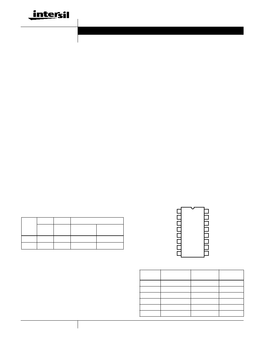
Pinout
DG411, DG412, DG413
(PDIP, SOIC)
TOP VIEW
TRUTH TABLE
LOGIC
DG411
DG412
DG413
SWITCH
SWITCH
SWITCH
1, 4
SWITCH
2, 3
0
ON
OFF
OFF
ON
1
OFF
ON
ON
OFF
NOTE:
Logic "0"
0.8V. Logic "1"
2.4V.
Ordering Information
PART
NUMBER
TEMP. RANGE
(
o
C)
PACKAGE
PKG. NO.
DG411DJ
-40 to 85
16 Ld PDIP
E16.3
DG411DY
-40 to 85
16 Ld SOIC
M16.15
DG412DJ
-40 to 85
16 Ld PDIP
E16.3
DG412DY
-40 to 85
16 Ld SOIC
M16.15
DG413DJ
-40 to 85
16 Ld PDIP
E16.3
DG413DY
-40 to 85
16 Ld SOIC
M16.15
14
15
16
9
13
12
11
10
1
2
3
4
5
7
6
8
IN
1
D
1
S
1
V-
GND
S
4
IN
4
D
4
IN
2
S
2
V+
V
L
S
3
D
3
IN
3
D
2
Data Sheet
June 1999
2
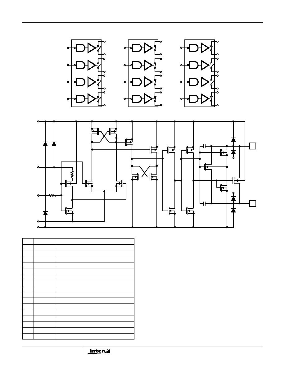
Functional Diagrams
Four SPST Switches per Package Switches Shown for Logic "1" Input
Schematic Diagram
(1 Channel)
S
1
D
1
S
2
D
2
S
3
D
3
S
4
D
4
DG411
S
1
D
1
S
2
D
2
S
3
D
3
S
4
D
4
IN
1
DG412
IN
2
IN
3
IN
4
S
1
D
1
S
2
D
2
S
3
D
3
S
4
D
4
IN
1
DG413
IN
2
IN
3
IN
4
IN
2
IN
3
IN
4
IN
1
S
V+
IN
X
GND
V-
V-
V
L
D
V+
Pin Descriptions
PIN
SYMBOL
DESCRIPTION
1
IN
1
Logic Control for Switch 1.
2
D
1
Drain (Output) Terminal for Switch 1.
3
S
1
Source (Input) Terminal for Switch 1.
4
V-
Negative Power Supply Terminal.
5
GND
Ground Terminal (Logic Common).
6
S
4
Source (Input) Terminal for Switch 4.
7
D
4
Drain (Output) Terminal for Switch 4.
8
IN
4
Logic Control for Switch 4.
9
IN
3
Logic Control for Switch 3.
10
D
3
Drain (Output) Terminal for Switch 3.
11
S
3
Source (Input) Terminal for Switch 3.
12
V
L
Logic Reference Voltage.
13
V+
Positive Power Supply Terminal (Substrate).
14
S
2
Source (Input) Terminal for Switch 2.
15
D
2
Drain (Output) Terminal for Switch 2.
16
IN
2
Logic Control for Switch 2.
DG411, DG412, DG413
3
Absolute Maximum Ratings
Thermal Information
V+ to V- . . . . . . . . . . . . . . . . . . . . . . . . . . . . . . . . . . . . . . . . . . . 44V
GND to V-. . . . . . . . . . . . . . . . . . . . . . . . . . . . . . . . . . . . . . . . . . 25V
V
L
. . . . . . . . . . . . . . . . . . . . . . . . . . . . . . (GND -0.3V) to (V+) +0.3V
Digital Inputs, V
S
, V
D
(Note 1). . . . . (V-) -2V to (V+) + 2V or 30mA,
Whichever Occurs First
Continuous Current (Any Terminal) . . . . . . . . . . . . . . . . . . . . . 30mA
Peak Current, S or D (Pulsed 1ms, 10% Duty Cycle Max) . . 100mA
Operating Conditions
Voltage Range . . . . . . . . . . . . . . . . . . . . . . . . . . . . . . . .
±
20V (Max)
Temperature Range . . . . . . . . . . . . . . . . . . . . . . . . . . -40
o
C to 85
o
C
Input Low Voltage . . . . . . . . . . . . . . . . . . . . . . . . . . . . . 0.8V (Max)
Input High Voltage . . . . . . . . . . . . . . . . . . . . . . . . . . . . . . 2.4V (Min)
Input Rise and Fall Time . . . . . . . . . . . . . . . . . . . . . . . . . . . .
20ns
Thermal Resistance (Typical, Note 2)
JA
(
o
C/W)
PDIP Package . . . . . . . . . . . . . . . . . . . . . . . . . . . . .
90
SOIC Package . . . . . . . . . . . . . . . . . . . . . . . . . . . . .
100
Maximum Junction Temperature (Plastic Packages) . . . . . . . .150
o
C
Maximum Storage Temperature Range . . . . . . . . . . -65
o
C to 150
o
C
Maximum Lead Temperature (Soldering 10s) . . . . . . . . . . . . 300
o
C
(SOIC - Lead Tips Only)
CAUTION: Stresses above those listed in "Absolute Maximum Ratings" may cause permanent damage to the device. This is a stress only rating and operation of the
device at these or any other conditions above those indicated in the operational sections of this specification is not implied.
NOTES:
1. Signals on S
X
, D
X
, or IN
X
exceeding V+ or V- will be clamped by internal diodes. Limit forward diode current to maximum current ratings.
2.
JA
is measured with the component mounted on an evaluation PC board in free air.
Electrical Specifications
Test Conditions: V+ = +15V, V- = -15V, V
L
= 5V, V
IN
= 2.4V, 0.8V (Note 3),
Unless Otherwise Specified
PARAMETER
TEST CONDITIONS
TEMP
(
o
C)
(NOTE 4)
MIN
(NOTE 5)
TYP
(NOTE 4)
MAX
UNITS
DYNAMIC CHARACTERISTICS
Turn-ON Time, t
ON
R
L
= 300
, C
L
= 35pF, V
S
=
±
10V (Figure 1)
25
-
110
175
ns
85
-
-
220
ns
Turn-OFF Time, t
OFF
25
-
100
145
ns
85
-
-
160
ns
Break-Before-Make Time Delay
DG413 Only, R
L
= 300
, C
L
= 35pF (Figure 2)
25
-
25
-
ns
Charge Injection, Q (Figure 3)
C
L
= 10nF, V
G
= 0V, R
G
= 0
25
-
5
-
pC
OFF Isolation (Figure 5)
R
L
= 50
, C
L
= 5pF, f = 1MHz
25
-
68
-
dB
Crosstalk (Channel-to-Channel),
(Figure 4)
25
-
-85
-
dB
Source OFF Capacitance, C
S(OFF)
f = 1MHz (Figure 6)
25
-
9
-
pF
Drain OFF Capacitance, C
D(OFF)
25
-
9
-
pF
Channel ON Capacitance,
C
D(ON)
+ C
S(ON)
25
-
35
-
pF
DIGITAL INPUT CHARACTERISTICS
Input Current V
IN
Low, I
IL
V
IN
Under Test = 0.8V, All Others = 2.4V
Full
-0.5
0.005
0.5
µ
A
Input Current V
IN
High, I
IH
V
IN
Under Test = 2.4V, All Others = 0.8V
Full
-0.5
0.005
0.5
µ
A
ANALOG SWITCH CHARACTERISTICS
Analog Signal Range, V
ANALOG
I
S
=
10mA
Full
-15
-
15
V
Drain-Source ON Resistance,
r
DS(ON)
I
S
=
10mA, V
D
=
±
8.5V, V+ = 13.5V, V- = -13.5V
25
-
25
35
Full
-
-
45
±
±
DG411, DG412, DG413

4
Source OFF Leakage Current,
I
S(OFF)
Drain OFF Leakage Current,
I
D(OFF)
V+ = 16.5V, V- = -16.5V, V
D
=
±
15.5V, V
S
=
15.5V
25
-0.25
±
0.1
0.25
nA
Full
-5
-
+5
nA
25
-0.25
±
0.1
0.25
nA
Full
-5
-
+5
nA
Channel ON Leakage Current,
I
D(ON)
+ I
S(ON)
V+ = 16.5V, V- = -16.5V, V
S
= V
D
=
±
15.5V
25
-0.4
±
0.1
0.4
nA
Full
-10
-
+10
nA
POWER SUPPLY CHARACTERISTICS
Positive Supply Current, I+
V+ = 16.5V, V- = -16.5V, V
IN
= 0V or 5V
25
-
0.0001
1
µ
A
85
-
5
µ
A
Negative Supply Current, I-
25
-1
-0.0001
-
µ
A
85
-5
-
-
µ
A
Logic Supply Current, I
L
25
-
0.0001
1
µ
A
85
-
-
5
µ
A
Ground Current, I
GND
25
-1
-0.0001
-
µ
A
85
-5
-
-
µ
A
Electrical Specifications
(Single Supply) Test Conditions: V+ = +12V, V- = 0V, V
L
= 5V, V
IN
= 2.4V, 0.8V (Note 3),
Unless Otherwise Specified
PARAMETER
TEST CONDITIONS
TEMP
(
o
C)
(NOTE 4)
MIN
(NOTE 5)
TYP
(NOTE 4)
MAX
UNITS
DYNAMIC CHARACTERISTICS
Turn-ON Time, t
ON
R
L
= 300
, C
L
= 35pF,
V
S
= 8V, (Figure 1)
25
-
175
250
ns
85
-
-
315
ns
Turn-OFF Time, t
OFF
25
-
95
125
ns
85
-
-
140
ns
Break-Before-Make Time Delay
DG413 Only, R
L
= 300
,
C
L
= 35pF, V
S
= 8V
25
-
25
-
ns
Charge Injection, Q
C
L
= 10nF, V
G
= 6.0V, R
G
= 0
25
-
25
-
pC
ANALOG SWITCH CHARACTERISTICS
Analog Signal Range, V
ANALOG
Full
0
-
12
V
Drain-Source ON Resistance,
r
DS(ON)
I
S
= -10mA, V
D
= 3V, 8V
V+ = 10.8V
25
-
40
80
Full
-
-
100
Electrical Specifications
Test Conditions: V+ = +15V, V- = -15V, V
L
= 5V, V
IN
= 2.4V, 0.8V (Note 3),
Unless Otherwise Specified (Continued)
PARAMETER
TEST CONDITIONS
TEMP
(
o
C)
(NOTE 4)
MIN
(NOTE 5)
TYP
(NOTE 4)
MAX
UNITS
±
DG411, DG412, DG413

5
POWER SUPPLY CHARACTERISTICS
Positive Supply Current, I+
V+ = 13.2V, V- = 0V
V
IN
= 0V or 5V
25
-
0.0001
1
µ
A
85
-
5
µ
A
Negative Supply Current, I-
25
-1
-0.0001
-
µ
A
85
-5
-
-
µ
A
Logic Supply Current, I
L
25
-
0.0001
1
µ
A
85
-
-
5
µ
A
Ground Current, I
GND
25
-1
-0.0001
-
µ
A
85
-5
-
-
µ
A
NOTES:
3. V
IN
= input voltage to perform proper function.
4. The algebraic convention whereby the most negative value is a minimum and the most positive a maximum, is used in this data sheet.
5. Typical values are for DESIGN AID ONLY, not guaranteed nor subject to production testing.
Test Circuits and Waveforms
V
O
is the steady state output with the switch on. Feedthrough via switch capacitance may result in spikes at the leading and trailing
edge of the output waveform.
NOTE: Logic input waveform is inverted for switches that have the
opposite logic sense.
FIGURE 1A. MEASUREMENTS POINTS
Repeat test for all IN and S.
For load conditions, see Specifications. C
L
includes fixture and stray
capacitance.
FIGURE 1B. TEST CIRCUIT
FIGURE 1. SWITCHING TIMES
FIGURE 2A. MEASUREMENT POINTS
FIGURE 2B. TEST CIRCUITS
FIGURE 2. BREAK-BEFORE-MAKE TIME
Electrical Specifications
(Single Supply) Test Conditions: V+ = +12V, V- = 0V, V
L
= 5V, V
IN
= 2.4V, 0.8V (Note 3),
Unless Otherwise Specified (Continued)
PARAMETER
TEST CONDITIONS
TEMP
(
o
C)
(NOTE 4)
MIN
(NOTE 5)
TYP
(NOTE 4)
MAX
UNITS
50%
t
r
< 20ns
t
f
< 20ns
t
OFF
90%
3V
0V
V
S
0V
t
ON
V
O
LOGIC
INPUT
SWITCH
INPUT
SWITCH
OUTPUT
90%
V
O
V
S
R
L
R
L
r
DS ON
(
)
+
------------------------------------
=
SWITCH
INPUT
LOGIC
INPUT
S
1
IN
1
V+
D
1
R
L
C
L
V
O
GND
V-
V
L
+15V
+5V
SWITCH
OUTPUT
-15V
t
D
3V
0V
V
S1
0V
t
D
LOGIC
INPUT
SWITCH
OUTPUT
SWITCH
OUTPUT
90%
0V
V
S2
(V01)
V
O2
90%
S
1
IN
1
, IN
2
V+
D
1
R
L1
C
L1
V
O1
GND
V-
V
L
V
S1
= 10V
300
+15V
+5V
35pF
S
2
D
2
R
L2
C
L2
V
O2
V
S2
= 10V
300
35pF
-15V
LOGIC
INPUT
C
L
includes fixture and
stray capacitance.
DG411, DG412, DG413