 | ÐлекÑÑоннÑй компоненÑ: DG412AK | СкаÑаÑÑ:  PDF PDF  ZIP ZIP |
Äîêóìåíòàöèÿ è îïèñàíèÿ www.docs.chipfind.ru
1
®
DG411/883, DG412/883
DG413/883
Monolithic Quad SPST CMOS Analog Switches
Features
· This Circuit is Processed in Accordance to MIL-STD-
883 and is Fully Conformant Under the Provisions of
Paragraph 1.2.1.
· ON-Resistance <35
Max
· Low Power Consumption (P
D
<35
µ
W)
· Fast Switching Action
- t
ON
<175ns
- t
OFF
<145ns
· Low Charge Injection
· Upgrade from DG211/DG212
· TTL, CMOS Compatible
· Single or Split Supply Operation
Applications
· Audio Switching
· Battery Operated Systems
· Data Acquisition
· Hi-Rel Systems
· Sample and Hold Circuits
· Communication Systems
· Automatic Test Equipment
Part Number Information
PART NUMBER
TEMP. RANGE
PACKAGE
DG411AK/883
-55
o
C to +125
o
C
16 Lead CerDIP
DG412AK/883
-55
o
C to +125
o
C
16 Lead CerDIP
DG413AK/883
-55
o
C to +125
o
C
16 Lead CerDIP
August 2003
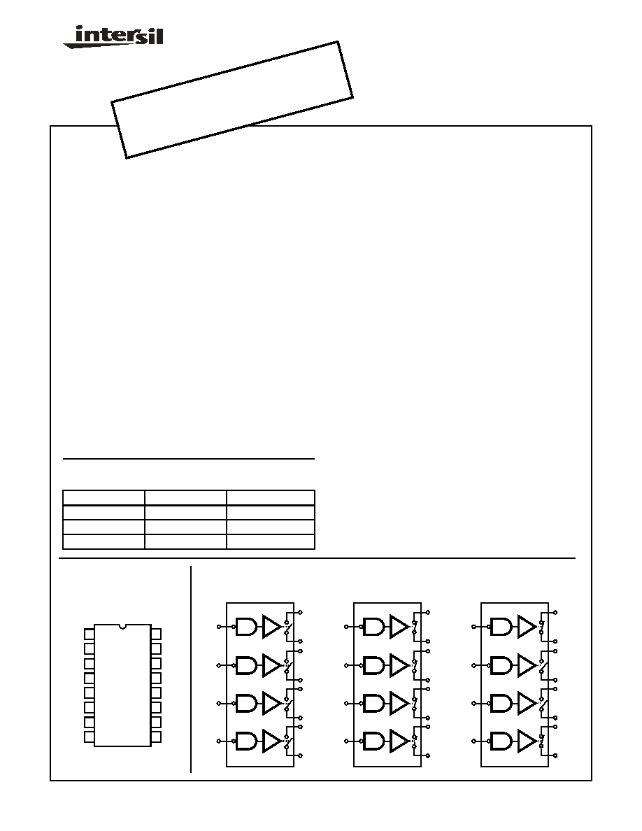
Pinout
DG411/883, DG412/883,
DG413/883 (CERDIP)
TOP VIEW
14
15
16
9
13
12
11
10
1
2
3
4
5
7
6
8
IN
1
D
1
S
1
V-
GND
S
4
IN
4
D
4
IN
2
S
2
V+
V
L
S
3
D
3
IN
3
D
2
(NC) NO CONNECTION
Functional Diagrams
Four SPST Switches per Package Switches Shown for Logic "1" Inpu
t
S
1
D
1
S
2
D
2
S
3
D
3
S
4
D
4
DG411/883
S
1
D
1
S
2
D
2
S
3
D
3
S
4
D
4
IN
1
DG412/883
IN
2
IN
3
IN
4
S
1
D
1
S
2
D
2
S
3
D
3
S
4
D
4
IN
1
DG413/883
IN
2
IN
3
IN
4
IN
2
IN
3
IN
4
IN
1
Description
The DG411/883 series monolithic CMOS analog switches
are drop-in replacements for the popular DG211 and DG212
series devices. They include four independent single pole
throw (SPST) analog switches, and TTL and CMOS compat-
ible digital inputs.
These switches feature lower analog ON resistance (<35
)
and faster switch time (t
ON
<175ns) compared to the DG211
or DG212. Charge injection has been reduced, simplifying
sample and hold applications.
The improvements in the DG411/883 series are made possi-
ble by using a high voltage silicon-gate process. An epitaxial
layer prevents the latch-up associated with older CMOS
technologies. The 44V maximum voltage range permits con-
trolling 40V
P-P
signals. Power supplies may be single-ended
from +5V to +34V, or split from
±
5V to
±
20V.
The four switches are bilateral, equally matched for AC or
bidirectional signals. The ON resistance variation with analog
signals is quite low over a
±
15V analog input range. The
switches in the DG411/883 and DG412/883 are identical, dif-
fering only in the polarity of the selection logic. Two of the
switches in the DG413/883 (#1 and #4) use the logic of the
DG211 and DG411/883 (i.e. a logic "0" turns the switch ON)
and the other two switches use DG212 and DG412/883 posi-
tive logic. This permits independent control of turn-on and
turn-off times for SPDT configurations, permitting "break-
before-make" or "make-before-break" operation with a mini-
mum of external logic.
Spec Number
512043
File Number
3681.1
OBSO
LETE
PRO
DUCT
NO R
ECOM
MEN
DED
REPL
ACEM
ENT
conta
ct ou
r Tec
hnica
l Sup
port
Cent
er at
1-888
-INTE
RSIL
or w
ww.in
tersil
.com
/tsc
CAUTION: These devices are sensitive to electrostatic discharge; follow proper IC Handling Procedures.
1-888-INTERSIL or 321-724-7143
|
Intersil (and design) is a registered trademark of Intersil Americas Inc.
Copyright © Intersil Americas Inc. 2003. All Rights Reserved
All other trademarks mentioned are the property of their respective owners.
2
DG411/883, DG412/883, DG413/883
Pin Description
PIN
SYMBOL
DESCRIPTION
1
IN
1
Logic Control for Switch 1
2
D
1
Drain (Output) Terminal for Switch 1
3
S
1
Source (Input) Terminal for Switch 1
4
V-
Negative Power Supply Terminal
5
GND
Ground Terminal (Logic Common)
6
S
4
Source (Input) Terminal for Switch 4
7
D
4
Drain (Output) Terminal for Switch 4
8
IN
4
Logic Control for Switch 4
9
IN
3
Logic Control for Switch 3
10
D
3
Drain (Output) Terminal for Switch 3
11
S
3
Source (Input) Terminal for Switch 3
12
V
L
Logic Reference Voltage
13
V+
Positive Power Supply Terminal (Substrate)
14
S
2
Source (Input) Terminal for Switch 2
15
D
2
Drain (Output) Terminal for Switch 2
16
IN
2
Logic Control for Switch 2
TRUTH TABLE
LOGIC
DG411/
883
DG412/
883
DG413/883
SWITCH
SWITCH
SWITCH
1, 4
SWITCH
2, 3
0
ON
OFF
OFF
ON
1
OFF
ON
ON
OFF
NOTE: Logic "0"
0.8V. Logic "1"
2.4V.
Spec Number
512043
3
Specifications DG411/883, DG412/883, DG413/883
Absolute Maximum Ratings
Thermal Information
V+ to V- . . . . . . . . . . . . . . . . . . . . . . . . . . . . . . . . . . . . . . . . . . . 44V
GND to V- . . . . . . . . . . . . . . . . . . . . . . . . . . . . . . . . . . . . . . . . . . 25V
V
L
(Note 2) . . . . . . . . . . . . . . . . . . . . . . . (GND -0.3V) to (V+) +0.3V
Digital Inputs, V
S
, V
D
(Note 2) . . . . . (V-) -2V to (V+) + 2V or 30mA,
Whichever Occurs First
Continuous Current (Any Terminal) . . . . . . . . . . . . . . . . . . . . . 30mA
Current, S or D (Pulsed 1ms, 10% Duty Cycle) . . . . . . . . . . . 100mA
Storage Temperature Range (A Suffix) . . . . . . . . . -65
o
C to +125
o
C
Lead Temperature (Soldering 10s). . . . . . . . . . . . . . . . . . . . +300
o
C
Thermal Resistance (Note 3)
JA
JC
CerDIP Package . . . . . . . . . . . . . . . . . . .
75
o
C/W
20
o
C/W
Junction Temperature . . . . . . . . . . . . . . . . . . . . . . . . . . . . . . +175
o
C
Operating Temperature (A Suffix) . . . . . . . . . . . . . . -55
o
C to +125
o
C
CAUTION: Stresses above those listed in "Absolute Maximum Ratings" may cause permanent damage to the device. This is a stress only rating and operation
of the device at these or any other conditions above those indicated in the operational sections of this specification is not implied.
Operating Conditions
Operating Voltage Range
. . . . . . . . . . . . . . . . . . . . . . . . . . . . ±
20V Max
Operating Temperature Range. . . . . . . . . . . . . . . . -55
o
C to +125
o
C
Input Low Voltage. . . . . . . . . . . . . . . . . . . . . . . . . . . . . . . . 0.8V Max
Input High Voltage. . . . . . . . . . . . . . . . . . . . . . . . . . . . . . . . 2.4V Min
Input Rise and Fall Time
. . . . . . . . . . . . . . . . . . . . . . . . . . . . . . . . .
20ns
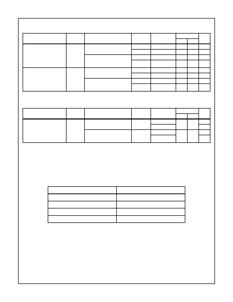
TABLE 1. DC ELECTRICAL PERFORMANCE CHARACTERISTICS
Device Tested at: V+ = +15V, V- = -15V, V
L
= 5V, GND = 0V, Unless Otherwise Specified
PARAMETERS
SYMBOL
CONDITIONS
GROUP A
SUBGROUP TEMPERATURE
LIMITS
UNITS
MIN
MAX
Drain-to-Source
ON Resistance
R
DS(ON)
V+ = +13.5V,
V- = -13.5V,
I
S
= -10mA,
V
D
=
±
8.5V
V
IN
= 0.8V
1, 3
+25
o
C, -55
o
C
0
35
DG411/883
2
+125
o
C
0
45
DG412/883
V
IN
= 2.4V
1, 3
+25
o
C, -55
o
C
0
35
2
+125
o
C
0
45
DG413/883
V
IN
= 0.8V or
2.4V (Note 1)
1, 3
+25
o
C, -55
o
C
0
35
2
+125
o
C
0
45
DG411/883
V+ = +10.8V,
V- = -0V,
I
S
= -10mA,
V
D
= 3.0V and
8.0V
V
IN
= 0.8V
1, 3
+25
o
C, -55
o
C
0
80
2
+125
o
C
0
100
DG412/883
V
IN
= 2.4V
1, 3
+25
o
C, -55
o
C
0
80
2
+125
o
C
0
100
DG413/883
V
IN
= 0.8V or
2.4V (Note 1)
1, 3
+25
o
C, -55
o
C
0
80
2
+125
o
C
0
100
Source OFF Leakage Current
I
S(OFF)
V+ = 16.5V,
V- = -16.5V,
V
D
= -15.5V,
V
S
= 15.5V
V
IN
= 2.4V
1
+25
o
C
-0.25
+0.25
nA
DG411/883
2, 3
+125
o
C, -55
o
C
-20
+20
nA
DG412/883
V
IN
= 0.8V
1
+25
o
C
-0.25
+0.25
nA
2, 3
+125
o
C, -55
o
C
-20
+20
nA
DG413/883
V
IN
= 0.8V or
2.4V (Note 1)
1
+25
o
C
-0.25
+0.25
nA
2, 3
+125
o
C, -55
o
C
-20
+20
nA
DG411/883
V+ = 16.5V,
V- = -16.5V,
V
D
= 15.5V,
V
S
= -15.5V
V
IN
= 2.4V
1
+25
o
C
-0.25
+0.25
nA
2, 3
+125
o
C, -55
o
C
-20
+20
nA
DG412/883
V
IN
= 0.8V
1
+25
o
C
-0.25
+0.25
nA
2, 3
+125
o
C, -55
o
C
-20
+20
nA
DG413/883
V
IN
= 0.8V or
2.4V (Note 1)
1
+25
o
C
-0.25
+0.25
nA
2, 3
+125
o
C, -55
o
C
-20
+20
nA
Spec Number
512043
4
Specifications DG411/883, DG412/883, DG413/883
Drain OFF Leakage Current
I
D(OFF)
V+ = 16.5V,
V- = -16.5V,
V
D
= -15.5V,
V
S
= 15.5V
V
IN
= 2.4V
1
+25
o
C
-0.25
+0.25
nA
DG411/883
2, 3
+125
o
C, -55
o
C
-20
+20
nA
DG412/883
V
IN
= 0.8V
1
+25
o
C
-0.25
+0.25
nA
2, 3
+125
o
C, -55
o
C
-20
+20
nA
DG413/883
V
IN
= 0.8V or
2.4V (Note 1)
1
+25
o
C
-0.25
+0.25
nA
2, 3
+125
o
C, -55
o
C
-20
+20
nA
DG411/883
V+ = 16.5V,
V- = -16.5V,
V
D
= 15.5V,
V
S
= -15.5V
V
IN
= 2.4V
1
+25
o
C
-0.25
+0.25
nA
2, 3
+125
o
C, -55
o
C
-20
+20
nA
DG412/883
V
IN
= 0.8V
1
+25
o
C
-0.25
+0.25
nA
2, 3
+125
o
C, -55
o
C
-20
+20
nA
DG413/883
V
IN
= 0.8V or
2.4V (Note 1)
1
+25
o
C
-0.25
+0.25
nA
2, 3
+125
o
C, -55
o
C
-20
+20
nA
Channel ON Leakage Current
I
D(ON) +
I
S(ON)
V+ = 16.5V,
V- = -16.5V,
V
S
= V
D
=
±
15.5V
V
IN
= 0.8V
1
+25
o
C
-0.4
+0.4
nA
DG411/883
2, 3
+125
o
C, -55
o
C
-40
+40
nA
DG412/883
V
IN
= 2.4V
1
+25
o
C
-0.4
+0.4
nA
2, 3
+125
o
C, -55
o
C
-40
+40
nA
DG413/883
V
IN
= 0.8V or
2.4V (Note 1)
1
+25
o
C
-0.4
+0.4
nA
2, 3
+125
o
C, -55
o
C
-40
+40
nA
Input Current with V
IN
Low
I
IL
Input Under Test = 0.8V,
All Others = 2.4V
1, 2, 3
+25
o
C, +125
o
C,
-55
o
C
-0.5
+0.5
µ
A
Input Current with V
IN
High
I
IH
Input Under Test = 2.4V,
All Others = 0.8V
1, 2, 3
+25
o
C, +125
o
C,
-55
o
C
-0.5
+0.5
µ
A
Positive Supply Current
I+
V+ = 16.5V, V- = -16.5,
V
IN
= 0Vor 5.0V
1
+25
o
C
-
+1.0
µ
A
2, 3
+125
o
C, -55
o
C
-
+5.0
µ
A
V+ = 13.2V, V- = 0V,
V
IN
= 0Vor 5.0V
V
L
= 5.25V
1
+25
o
C
-
+1.0
µ
A
2, 3
+125
o
C, -55
o
C
-
+5.0
µ
A
Negative Supply Current
I-
V+ = 16.5V, V- = -16.5,
V
IN
= 0V or 5.0V
1
+25
o
C
-1.0
-
µ
A
2, 3
+125
o
C, -55
o
C
-5.0
-
µ
A
V+ = 13.2V, V- = 0V,
V
IN
= 0V or 5.0V
V
L
= 5.25V
1
+25
o
C
-1.0
-
µ
A
2, 3
+125
o
C, -55
o
C
-5.0
-
µ
A
Logic Supply Current
I
L
V+ = 16.5V, V- = -16.5,
V
IN
= 0V or 5.0V
1
+25
o
C
-
+1.0
µ
A
2, 3
+125
o
C, -55
o
C
-
+5.0
µ
A
V+ = 13.2V, V- = 0V,
V
IN
= 0V or 5.0V
V
L
= 5.25V
1
+25
o
C
-
+1.0
µ
A
2, 3
+125
o
C, -55
o
C
-
+5.0
µ
A
Ground Current
I
GND
V+ = 16.5V, V- = -16.5,
V
IN
= 0V or 5.0V
1
+25
o
C
-1.0
-
µ
A
2, 3
+125
o
C, -55
o
C
-5.0
-
µ
A
V+ = 13.2V, V- = 0V,
V
IN
= 0V or 5.0V
V
L
= 5.25V
1
+25
o
C
-1.0
-
µ
A
2, 3
+125
o
C, -55
o
C
-5.0
-
µ
A
TABLE 1. DC ELECTRICAL PERFORMANCE CHARACTERISTICS (Continued)
Device Tested at: V+ = +15V, V- = -15V, V
L
= 5V, GND = 0V, Unless Otherwise Specified
PARAMETERS
SYMBOL
CONDITIONS
GROUP A
SUBGROUP TEMPERATURE
LIMITS
UNITS
MIN
MAX
Spec Number
512043
5
Specifications DG411/883, DG412/883, DG413/883
TABLE 2. AC ELECTRICAL PERFORMANCE CHARACTERISTICS
Device Tested at: V+ = +15V, V- = -15V, V
L
= 5V, GND = 0V, Unless Otherwise Specified
PARAMETERS
SYMBOL
CONDITIONS
GROUP A
SUBGROUP TEMPERATURE
LIMITS
UNITS
MIN
MAX
Turn ON Time
t
ON
C
L
= 35pF, V
S
=
±
10V,
R
L
= 300
9, 11
+25
o
C, -55
o
C
0
175
ns
10
+125
o
C
0
240
ns
V+ = 12V, V- = 0V,
C
L
= 35pF, V
S
= +8V,
R
L
= 300
9, 11
+25
o
C, -55
o
C
0
250
ns
10
+125
o
C
0
400
ns
Turn OFF Time
t
OFF
C
L
= 35pF, V
S
=
±
10V,
R
L
= 300
9, 11
+25
o
C, -55
o
C
0
145
ns
10
+125
o
C
0
160
ns
V+ = 12V, V- = 0V,
C
L
= 35pF, V
S
= +8V,
R
L
= 300
9, 11
+25
o
C, -55
o
C
0
125
ns
10
+125
o
C
0
140
ns
TABLE 3. ELECTRICAL PERFORMANCE CHARACTERISTICS (NOTE 1)
Device Tested at: V+ = +15V, V- = -15V, V
L
= 5V, GND = 0V, Unless Otherwise Specified
PARAMETERS
SYMBOL
CONDITIONS
GROUP A
SUBGROUP TEMPERATURE
LIMITS
UNITS
MIN
MAX
Charge Injection
Q
See Figure 2, V
G
= 0V, R
G
= 0
,
T
A
= +25
o
C, C
L
= 10nF
9
+25
o
C
-100
+100
pC
+25
o
C
pC
See Figure 2,
V
G
= 6V, R
G
= 0
, T
A
= +25
o
C
C
L
= 10nF, V+ = 12V, V- = 0V
9
+25
o
C
-100
+100
pC
+25
o
C
pC
NOTES:
1. V
IN
= Input Voltage to Perform Proper Function.
2. Signals on S
X
, D
X
or IN
X
exceeding V+ or V- will be clamped by internal diodes. Limit forward diode current to maximum current ratings.
3. All leads soldered or welded to PC board.
4. Parameters listed in Table 3 are controlled via design or process and are not directly tested at final production. These parameters are lab
characterized upon initial design release or upon design changes. These parameters are guaranteed by characterization based upon
data from multiple production runs which reflect lot to lot and within lot variation.
TABLE 4. ELECTRICAL TEST REQUIREMENTS
MIL-STD-883 TEST REQUIREMENTS
SUBGROUPS (SEE TABLES 1 AND 2)
Interim Electrical Parameters (Pre Burn-In)
1
Final Electrical Test Parameters
1 (Note 1), 2, 3, 9, 10, 11
Group A Test Requirements
1, 2, 3, 9, 10, 11
Groups C and D Endpoints
1
NOTE:
1. PDA applies to Subgroup 1 only.
Spec Number
512043