 | –≠–ª–µ–∫—Ç—Ä–æ–Ω–Ω—ã–π –∫–æ–º–ø–æ–Ω–µ–Ω—Ç: DG506AA | –°–∫–∞—á–∞—Ç—å:  PDF PDF  ZIP ZIP |
1
File Number
3137.4
DG508A
CMOS Analog Multiplexers
The DG508A is a CMOS Monolithic 8-Channel Analog
Multiplexer, which can also be used as a demultiplexer. An
enable input is provided. When the enable input is high, a
channel is selected by the address inputs, and when low, all
channels are off.
A channel in the ON state conducts current equally well in
both directions. In the OFF state each channel blocks
voltages up to the supply rails. The address inputs and the
enable input are TTL and CMOS compatible over the full
specified operating temperature range.
The DG508A is pinout compatible with the industry standard
devices.
Features
∑ Low Power Consumption
∑ TTL and CMOS-Compatible Address and Enable Inputs
∑ 44V Maximum Power Supply Rating
∑ High Latch-Up Immunity
∑ Break-Before-Make Switching
∑ Alternate Source
Applications
∑ Data Acquisition Systems
∑ Communication Systems
∑ Signal Multiplexing/Demultiplexing
∑ Audio Signal Multiplexing
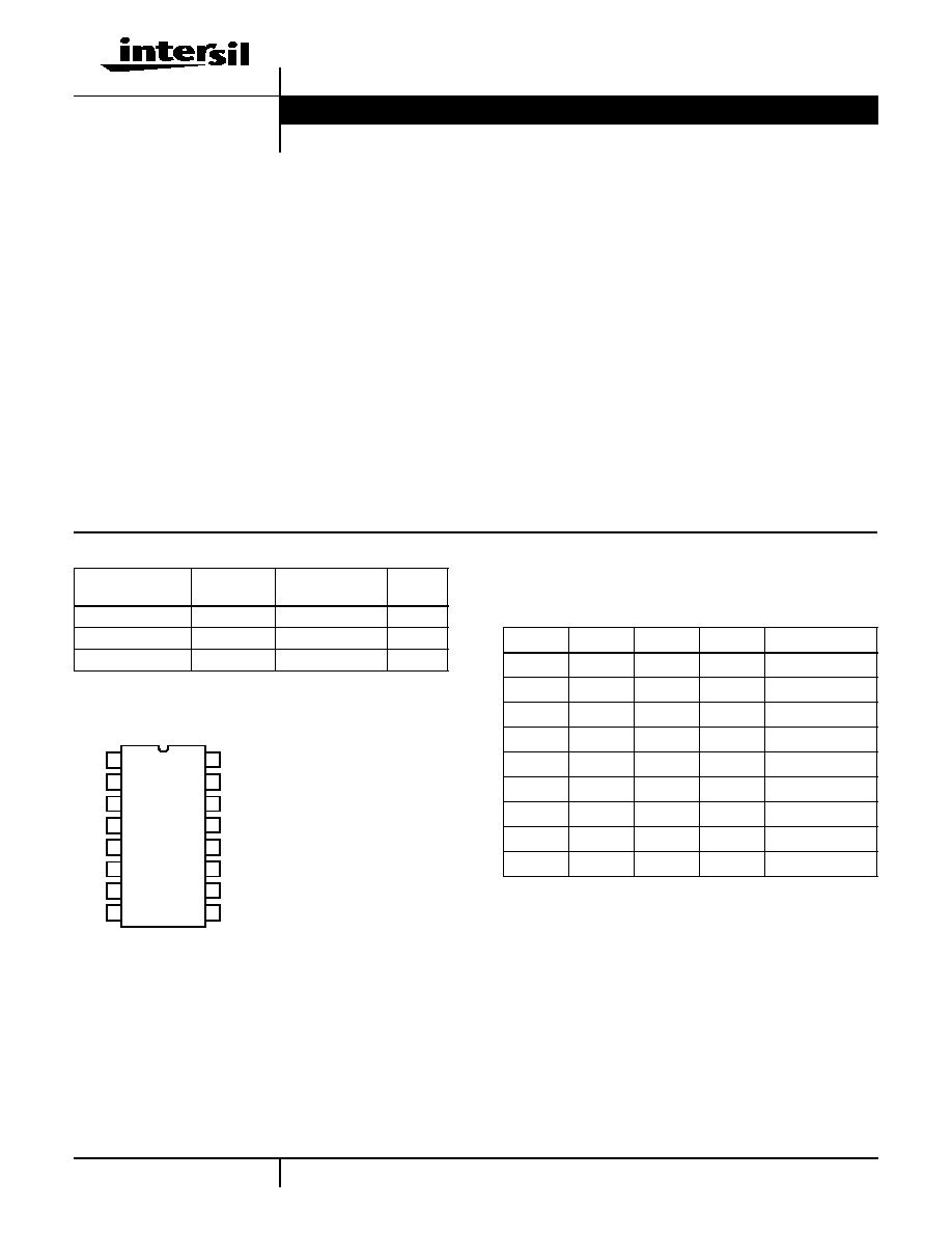
Ordering Information
Truth Table
PART NUMBER
TEMP.
RANGE (
o
C)
PACKAGE
PKG.
NO.
DG508AAK
-55 to 125
16 Ld CERDIP
F16.3
DG508ABK
-25 to 85
16 Ld CERDIP
F16.3
DG508ACJ
0 to 70
16 Ld PDIP
E16.3
Pinout
DG508A (PDIP, CERDIP)
TOP VIEW
14
15
16
9
13
12
11
10
1
2
3
4
5
7
6
8
A
0
EN
V-
S
1
S
2
S
3
D
S
4
A
1
GND
V+
S
5
S
6
S
7
S
8
A
2
DG508A
A
2
A
1
A
0
EN
ON SWITCH
X
X
X
0
None
0
0
0
1
1
0
0
1
1
2
0
1
0
1
3
0
1
1
1
4
1
0
0
1
5
1
0
1
1
6
1
1
0
1
7
1
1
1
1
8
A
0
, A
1
, A
2
, EN
Logic "1" = V
AH
2.4V, Logic "0" = V
AL
0.8V
Data Sheet
June 2001
itle
G50
,
507
508
509
b-
t
MO
na-
lti-
x-
)
utho
)
ey-
rds
ter-
rpo-
ion,
i-
n-
ctor,
lti-
xer,
x,
an-
l,
ched
eo)
re-
r ()
CAUTION: These devices are sensitive to electrostatic discharge; follow proper IC Handling Procedures.
1-888-INTERSIL or 321-724-7143
|
Intersil and Design is a trademark of Intersil Americas Inc.
|
Copyright © Intersil Americas Inc. 2001
2
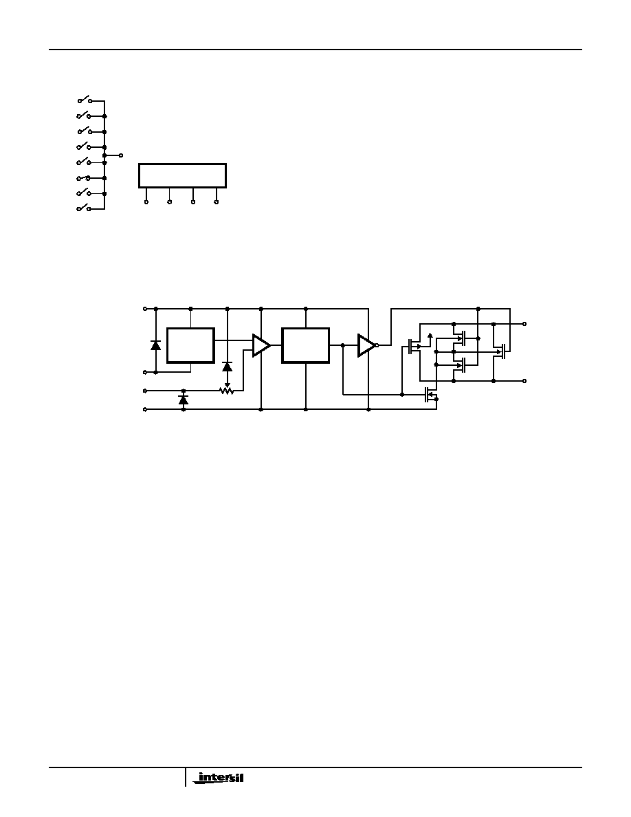
Schematic Diagram
Functional Diagram
DG508A
3 Line Binary Address Inputs
(1 0 1) and EN = 1
Above example shows channel 6 turned ON.
S
1
S
3
S
2
S
4
S
5
S
6
S
7
S
8
A
0
D
ADDRESS DECODER
1 OF 8
A
1
A
2
EN (ENABLE INPUT)
LOGIC TRIP
POINT REF
LOGIC INTERFACE
AND LEVEL SHIFTER
+
-
DECODER
A
X
V+
TYPICAL
SWITCH
S
X
D
X
V+
GND
LOGIC A
X
INPUT OR EN
V-
DG508A

3
Absolute Maximum Ratings
Thermal Information
V+ to V- . . . . . . . . . . . . . . . . . . . . . . . . . . . . . . . . . . . . . . . . . . . 44V
V- to Ground. . . . . . . . . . . . . . . . . . . . . . . . . . . . . . . . . . . . . . . . 25V
Digital Inputs, V
S
, V
D
(Note 1). . . . . . . . . . . . . (V- -2V) To (V+ +2V)
Continuous Current, (Any Terminal Except S or D) . . . . . . . . . 30mA
Continuous Current, (S or D) . . . . . . . . . . . . . . . . . . . . . . . . . . 20mA
Peak Current, S or D (Pulsed 1ms, 10% Duty Cycle Max) . . . . . 40mA
Operating Conditions
Temperature Range
"A" Suffix. . . . . . . . . . . . . . . . . . . . . . . . . . . . . . . . -55
o
C to 125
o
C
"B" Suffix. . . . . . . . . . . . . . . . . . . . . . . . . . . . . . . . . -25
o
C to 85
o
C
"C" Suffix . . . . . . . . . . . . . . . . . . . . . . . . . . . . . . . . . 0
o
C to 70
o
C
Thermal Resistance (Typical, Note 2)
JA
(
o
C/W)
JC
(
o
C/W)
16 Ld CERDIP Package. . . . . . . . . . . .
75
20
16 Ld PDIP Package . . . . . . . . . . . . . .
90
N/A
Maximum Junction Temperature
CERDIP Package. . . . . . . . . . . . . . . . . . . . . . . . . . . . . . . . .175
o
C
PDIP Package . . . . . . . . . . . . . . . . . . . . . . . . . . . . . . . . . . . 150
o
C
Maximum Storage Temperature
"A" and "B" Suffix . . . . . . . . . . . . . . . . . . . . . . . . . -65
o
C to 150
o
C
"C" Suffix . . . . . . . . . . . . . . . . . . . . . . . . . . . . . . . -65
o
C to 125
o
C
Maximum Lead Temperature (Soldering 10s) . . . . . . . . . . . . . 300
o
C
CAUTION: Stresses above those listed in "Absolute Maximum Ratings" may cause permanent damage to the device. This is a stress only rating and operation of the
device at these or any other conditions above those indicated in the operational sections of this specification is not implied.
NOTES:
1. Signals on S
X
, D, E
N
, or A
X
exceeding V+ or V- are clamped by internal diodes. Limit diode current to maximum current ratings.
2.
JA
is measured with the component mounted on an evaluation PC board in free air.
Electrical Specifications
T
A
= 25
o
C, V+ = +15V, V- = -15V, GND = 0V, V
EN
= 2.4V, Unless Otherwise Specified
PARAMETER
TEST CONDITIONS
"A" SUFFIX
"B" AND "C" SUFFIX
UNITS
(NOTE 4)
MIN
(NOTE 3)
TYP
(NOTE 4)
MAX
(NOTE 4)
MIN
(NOTE 3)
TYP
(NOTE 4)
MAX
DYNAMIC CHARACTERISTICS
Switching Time of
Multiplexer, t
TRANSITION
See Figure 1
-
0.6
1
-
0.6
-
µ
s
Break-Before-Make
Interval, t
OPEN
See Figure 3
-
0.2
-
-
0.2
-
µ
s
Enable Turn-ON Time,
t
ON(EN)
See Figure 2
-
1
1.5
-
1
-
µ
s
Enable Turn-OFF Time,
t
OFF(EN)
See Figure 2
-
0.4
1.0
-
0.4
-
µ
s
OFF Isolation, OIRR
V
EN
= 0V, R
L
= 1k
, C
L
= 15pF,
V
S
= 7V
RMS
, f = 500kHz (Note 5)
-
68
-
-
68
-
dB
Source OFF Capacitance,
C
S(OFF)
V
S
= 0V, V
EN
= 0V, f = 140kHz
-
5
-
-
5
-
pF
Drain OFF Capacitance,
C
D(OFF)
V
D
= 0V, V
EN
= 0V, f = 140kHz
-
25
-
-
25
-
pF
Charge Injection, Q
See Figure 4
-
4
-
-
4
-
pC
DIGITAL INPUT CHARACTERISTICS
Address Input Current,
Input Voltage High, I
AH
V
A
= 2.4V
-10
-0.002
-
-10
-0.002
-
µ
A
V
A
= 15V
-
0.006
10
-
0.006
10
µ
A
Address Input Current Input
Voltage Low, I
AL
V
EN
= 2.4V
V
A
= 0V
-10
-0.002
-
-10
-0.002
-
µ
A
V
EN
= 0V
-10
-0.002
-
-10
-0.0002
-
µ
A
ANALOG SWITCH CHARACTERISTICS
Analog Signal Range,
V
ANALOG
(Note 7)
-15
-
+15
-15
-
+15
V
Drain-Source ON
Resistance, r
DS(ON)
Sequence Each
Switch ON
V
AL
= 0.8V,
V
AH
= 2.4V
I
S
= -200
µ
A, V
D
= +10V
-
270
400
-
270
450
I
S
= -200
µ
A, V
D
= -10V
-
230
400
-
230
450
r
DS(ON)
Matching
Between Channels
-10V
V
S
+10V
-
6
-
-
6
-
%
r
D S ON
(
)
r
DS(ON)MAX
r
DS ON
(
)
MI N
≠
r
DS ON
(
)
AVG
-----------------------------------------------------------------------
=
DG508A

4
Source OFF Leakage
Current, I
S(OFF)
V
EN
= 0V
V
S
= +10V, V
D
= -10V
-1
0.002
1
-5
0.002
5
nA
V
S
= -10V, V
D
= +10V
-1
-0.005
1
-5
-0.005
5
nA
Drain OFF Leakage
Current, I
D(OFF)
V
EN
= 0V
V
S
= -10V, V
D
= +10V
-
0.01
10
-
0.01
20
nA
V
S
= +10V, V
D
= -10V
-10
-0.015
-
-20
-0.015
-
nA
Drain ON Leakage Current,
I
D(ON)
(Note 6)
Sequence Each
Switch ON
V
AL
= 0.8V,
V
AH
= 2.4V
V
D
= V
S(ALL)
= +10V
-
0.015
10
-
0.015
20
nA
V
D
= V
S(ALL)
= -10V
-10
-0.03
-
-20
-0.03
-
nA
POWER SUPPLY CHARACTERISTICS
Positive Supply Current, I+
V
EN
= 5.0V (Enabled) or
V
EN
= 0V (Standby), V
A
= 0V
-
1.3
2.4
-
1.3
2.4
mA
Negative Supply Current, I-
-1.5
-0.7
-
-1.5
-0.7
-
mA
Electrical Specifications
T
A
= 25
o
C, V+ = +15V, V- = -15V, GND = 0V, V
EN
= 2.4V, Unless Otherwise Specified
(Continued)
PARAMETER
TEST CONDITIONS
"A" SUFFIX
"B" AND "C" SUFFIX
UNITS
(NOTE 4)
MIN
(NOTE 3)
TYP
(NOTE 4)
MAX
(NOTE 4)
MIN
(NOTE 3)
TYP
(NOTE 4)
MAX
Electrical Specifications
T
A
= Over Operating Temperature Range, V+ = +15V, V- = -15V, GND = 0V, V
EN
= 2.4V,
Unless Otherwise Specified
PARAMETER
TEST CONDITIONS
"A" SUFFIX
UNITS
MIN
(NOTE 3)
TYP
MAX
DIGITAL INPUT CHARACTERISTICS
Address Input Current, Input Voltage
High, I
AH
V
A
= 2.4V
-30
-
-
µ
A
V
A
= 15V
-
-
30
µ
A
Address Input Current Input Voltage
Low, I
AL
V
EN
= 2.4V
V
A
= 0V
-30
-
-
µ
A
V
EN
= 0V
-30
-
-
µ
A
ANALOG SWITCH CHARACTERISTICS
Analog Signal Range, V
ANALOG
(Note 7)
-15
-
+15
V
Drain-Source ON Resistance, r
DS(ON)
Sequence Each Switch ON
V
AL
= 0.8V, V
AH
= 2.4V
I
S
= -200
µ
A, V
D
= +10V
-
-
500
I
S
= -200
µ
A, V
D
= -10V
-
-
500
Source OFF Leakage Current, I
S(OFF)
V
EN
= 0V
V
S
= +10V, V
D
= -10V
-
-
50
nA
V
S
= -10V, V
D
= +10V
-50
-
-
nA
Drain OFF Leakage Current, I
D(OFF)
V
EN
= 0V
V
S
= -10V, V
D
= +10V
-
-
200
nA
V
S
= +10V, V
D
= -10V
-200
-
-
nA
Drain ON Leakage Current, I
D(ON)
(Note 6) Sequence Each Switch ON
V
AL
= 0.8V, V
AH
= 2.4V
V
D
= V
S(ALL)
= +10V
-
-
200
nA
V
D
= V
S(ALL)
= -10V
-200
-
-
nA
POWER SUPPLY CHARACTERISTICS
Positive Supply Current, I+
V
EN
= 5.0V, V
A
= 0V
-3.2
-
4.5
mA
Negative Supply Current, I-
-3.2
-
4.5
mA
Positive Standby Supply Current, I+
V
EN
= 0V, V
A
= 0V
-3.2
-
4.5
mA
Negative Standby Supply Current, I-
-3.2
-
4.5
mA
NOTES:
3. Typical values are for design aid only, not guaranteed and not subject to production testing.
4. The algebraic convention whereby the most negative value is a minimum, and the most positive value is a maximum, is used in this data sheet.
5. Off isolation = 20Log | V
S
|/| V
D
|, where V
S
= input to Off switch, and V
D
= output due to V
S
.
6. I
D(ON)
is leakage from driver into "ON" switch.
7. Parameter not tested. Parameter guaranteed by design or characterization.
DG508A
5
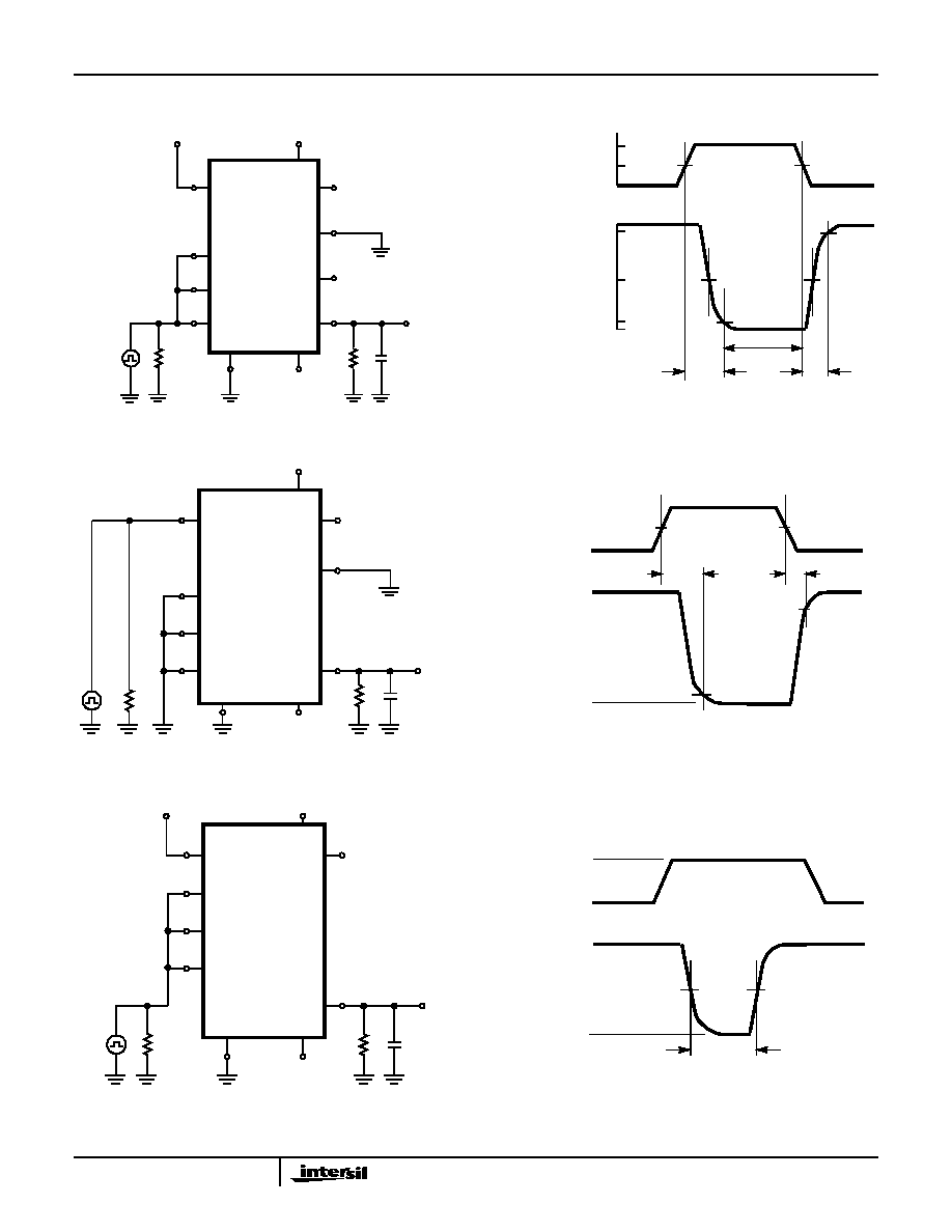
Test Circuits and Waveforms
FIGURE 1A. TEST CIRCUIT
FIGURE 1B. MEASUREMENT POINTS
FIGURE 1. SWITCHING TIME
FIGURE 2A. TEST CIRCUIT
FIGURE 2B. MEASUREMENT POINTS
FIGURE 2. ENABLE TIMES
FIGURE 3A. TEST CIRCUIT
FIGURE 3B. MEASUREMENT POINTS
FIGURE 3. BREAK-BEFORE-MAKE INTERVAL
EN
A
2
S
2
THRU S
7
A
1
A
0
LOGIC
INPUT
50
+2.4V
SWITCH
OUTPUT
35pF
1M
+15V
-15V
-10V
+10V
GND
V-
DG508A
S
1
S
8
D
V+
V
O
3V
50%
0
V
S1
0.8V
S1
0
0.8V
S8
V
S8
SWITCH
OUTPUT
V
O
TRANSITION
S
1
ON
S
8
ON
LOGIC INPUT
t
r
< 20ns
t
f
< 20ns
TIME
TRANSITION
TIME
EN
A
2
S
2
THRU S
8
A
1
A
0
EN
50
SWITCH
OUTPUT
35pF
1k
+15V
-15V
GND
V-
DG508A
S
1
D
V+
V
O
-5V
3V
50%
0V
SWITCH
OUTPUT
V
O
t
r
< 20ns
t
f
< 20ns
0V
V
O
t
ON (EN)
t
OFF (EN)
EN
50%
0.9V
O
0.1V
O
EN
A
1
A
2
LOGIC
INPUT
50
+2.4V
SWITCH
OUTPUT
35pF
1k
+15V
-15V
GND
V-
DG508A
S
1
THRU S
8
D
V+
V
O
A
0
+5V (V
S
)
3V
50%
0V
SWITCH
OUTPUT
V
O
t
r
< 20ns
t
f
< 20ns
0V
LOGIC
t
OPEN
INPUT
50%
V
S
DG508A