12-1
Semiconductor
Features
∑ Direct RESET
∑ TTL and CMOS Compatible Address and Enable
Inputs
∑ Maximum Power Supply Rating . . . . . . . . . . . . . . . . 44V
∑ Break-Before-Make Switching
∑ Alternate Source
Applications
∑ Data Acquisition Systems
∑ Communication Systems
∑ Automatic Test Equipment
∑ Microprocessor Controlled Systemd
Description
The DG526, DG527, DG528, and DG529 are CMOS
Monolithic 16-Channel/Dual 4-Channel Analog Multiplexers.
Each device has on-chip address and control latches to sim-
plify design in microprocessor based applications. The DG526
uses 4 address lines to control its 16 channels; the DG527,
DG528 both use 3 address lines to control their 8 channels;
and the DG529 uses 2 address lines to control its 4 channels.
The enable pin is used to enable the address latches during
the WR pulse. It can be hard wired to the logic supply if one of
the channels will always be used (except during a reset) or it
can be tied to address decoding circuitry for memory mapped
operation. The RS pin is used to clear all latches regardless of
the state of any other latch or control line. The WR pin is used
to transfer the state of the address control lines to their
latches, except during a reset or when EN is low.
A channel in the ON state conducts signals equally well in
both directions. In the OFF state each channel blocks volt-
ages up to the supply rails. The address inputs, WR, RS and
the enable input are TTL and CMOS compatible over the full
specified operation temperature range.
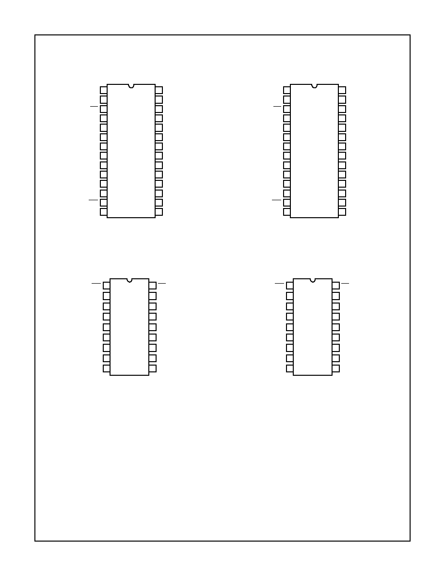
Part Number Information
PART
NUMBER
TEMP.
RANGE (
o
C)
PACKAGE
PKG. NO.
DG526AK
-55 to 125
28 Ld CERDIP
F28.6
DG526AK/883B
-55 to 125
28 Ld CERDIP
F28.6
DG526BK
-25 to 85
28 Ld CERDIP
F28.6
DG526BY
-25 to 85
28 Ld SOIC
M28.3
DG526CJ
0 to 70
28 Ld PDIP
E28.6
DG526CK
0 to 70
28 Ld CERDIP
F28.6
DG526CY
0 to 70
28 Ld SOIC
M28.3
DG527AK
-55 to 125
28 Ld CERDIP
F28.6
DG527AK/883B
-55 to 125
28 Ld CERDIP
F28.6
DG527BK
-25 to 85
28 Ld CERDIP
F28.6
DG527BY
-25 to 85
28 Ld SOIC
M28.3
DG527CJ
0 to 70
28 Ld PDIP
E28.6
DG527CK
0 to 70
28 Ld CERDIP
F28.6
DG527CY
0 to 70
28 Ld SOIC
M28.3
DG528AK
-55 to 125
18 Ld CERDIP
F18.3
DG528AK/883B
-55 to 125
18 Ld CERDIP
F18.3
DG528BK
-25 to 85
18 Ld CERDIP
F18.3
DG528BY
-25 to 85
18 Ld SOIC
M18.3
DG528CJ
0 to 70
18 Ld PDIP
E18.3
DG528CK
0 to 70
18 Ld CERDIP
F18.3
DG528CY
0 to 70
18 Ld SOIC
M18.3
DG529AK
-55 to 125
18 Ld CERDIP
F18.3
DG529AK/883B
-55 to 125
18 Ld CERDIP
F18.3
DG529BK
-25 to 85
18 Ld CERDIP
F18.3
DG529BY
-25 to 85
18 Ld SOIC
M18.3
DG529CJ
0 to 70
18 Ld PDIP
E18.3
DG529CK
0 to 70
18 Ld CERDIP
F18.3
DG529CY
0 to 70
18 Ld SOIC
M18.3
PART
NUMBER
TEMP.
RANGE (
o
C)
PACKAGE
PKG. NO.
April 1999
CAUTION: These devices are sensitive to electrostatic discharge. Users should follow proper IC Handling Procedures.
Copyright
©
Harris Corporation 1999
DG526, DG527,
DG528, DG529
Analog CMOS
Latchable Multiplexers
File Number
3139.2
FOR A POSSIBLE SUBSTITUTE PR
ODUCT
call Central Applications 1-800-442-7747
or email: centapp@harris.com
OBSOLETE PR
ODUCT

12-3
Functional Diagrams
DG526
16-CHANNEL SINGLE ENDED MULTIPLEXER
DG527
DIFFERENTIAL 8-CHANNEL MULTIPLEXER
DG528
8-CHANNEL SINGLE ENDED MULTIPLEXER
DG529
DUAL 4-CHANNEL MULTIPLEXER
S
1
S
2
S
3
S
4
S
5
S
6
S
7
S
8
S
9
S
10
S
11
S
12
S
13
S
14
S
15
S
16
WR
RS
D
V+
V-
GND
EN
A
3
A
2
A
1
A
0
DECODER LOGIC AND LATCHES
S
1A
S
2A
S
3A
S
4A
S
5A
S
6A
S
7A
S
8A
S
1B
S
2B
S
3B
S
4B
S
5B
S
6B
S
7B
S
8B
WR
RS
D
A
V+
V-
GND
EN
A
2
A
1
A
0
DECODER LOGIC AND LATCHES
D
B
S
1
S
2
S
3
S
4
S
5
S
6
S
7
S
8
WR
A
2
A
1
A
0
DECODER LOGIC AND LATCHES
EN
RS
LATCHES
D
V+
V-
GND
S
1A
S
2A
S
3A
S
4A
WR
A
0
DECODER LOGIC
EN
RS
LATCHES
S
1B
S
2B
S
3B
S
4B
D
B
A
0
DECODER LOGIC AND LATCHES
D
A
V+
V-
GND
DG526, DG527, DG528, DG529

12-5
Absolute Maximum Ratings
Thermal Information
V+ to V-. . . . . . . . . . . . . . . . . . . . . . . . . . . . . . . . . . . . . . . . . . . +44V
V- to Ground . . . . . . . . . . . . . . . . . . . . . . . . . . . . . . . . . . . . . . . .-25V
V
IN
to Ground (Note 1) . . . . . . . . . . . . . . . . . . . . (V- - 2V), (V+ + 2V)
V
S
or V
D
to V+ (Note 1) . . . . . . . . . . . . . . . . . . . . . . . . +2V, (V- - 2V)
V
S
or V
D
to V- (Note 1). . . . . . . . . . . . . . . . . . . . . . . . -2V, (V+ + 2V)
Current, Any Terminal Except S or D . . . . . . . . . . . . . . . . . . . . 30mA
Continuous Current, S or D . . . . . . . . . . . . . . . . . . . . . . . . . . . 20mA
Peak Current, S or D . . . . . . . . . . . . . . . . . . . . . . . . . . . . . . . . 40mA
(Pulsed at 1ms, 10% Duty Cycle Max)
Operating Conditions
Operating Temperature
C Suffix . . . . . . . . . . . . . . . . . . . . . . . . . . . . . . . . . . . .0
o
C to 70
o
C
B Suffix . . . . . . . . . . . . . . . . . . . . . . . . . . . . . . . . . . -25
o
C to 85
o
C
A Suffix . . . . . . . . . . . . . . . . . . . . . . . . . . . . . . . . . -55
o
C to 125
o
C
Thermal Resistance (Typical, Note 1)
JA
(
o
C/W)
JC
(
o
C/W)
18 Ld PDIP Package . . . . . . . . . . . . . .
90
N/A
18 Ld CERDIP Package . . . . . . . . . . .
75
22
18 Ld SOIC Package . . . . . . . . . . . . . .
95
N/A
28 Ld PDIP Package . . . . . . . . . . . . . .
60
N/A
28 Ld CERDIP Package . . . . . . . . . . .
55
18
28 Ld SOIC Package . . . . . . . . . . . . . .
70
N/A
Maximum Junction Temperature
Ceramic Packages. . . . . . . . . . . . . . . . . . . . . . . . . . . . . . . . 175
o
C
Plastic Packages . . . . . . . . . . . . . . . . . . . . . . . . . . . . . . . . . 150
o
C
Maximum Storage Temperature Range
C Suffix . . . . . . . . . . . . . . . . . . . . . . . . . . . . . . . . .-65
o
C to 125
o
C
A and B Suffix . . . . . . . . . . . . . . . . . . . . . . . . . . . .-65
o
C to 150
o
C
Maximum Lead Temperature (Soldering 10s) . . . . . . . . . . . . . 300
o
C
(SOIC - Lead Tips Only)
CAUTION: Stresses above those listed in "Absolute Maximum Ratings" may cause permanent damage to the device. This is a stress only rating and operation of
the device at these or any other conditions above those indicated in the operational sections of this specification is not implied.
NOTE:
1.
JA
is measured with the component mounted on an evaluation PC board in free air.
Electrical Specifications
(Note 3) V+ = +15V, V- = -15V, GND = 0V, WR = 0V, RS = 2.4V, EN = 2.4V, T
A
= 25
o
C,
Unless Otherwise Specified
PARAMETER
(NOTE 6)
TEST CONDITIONS
A SUFFIX
B AND C SUFFIX
UNITS
MIN
(NOTE 2)
TYP
MAX
MIN
(NOTE 2)
TYP
MAX
DYNAMIC
Switching Time
of Multiplexer,
t
TRANSITION
DG526,
DG527
See Figure 3 (Note 7)
-
0.65
1
-
0.65
-
µ
s
DG528,
DG529
See Figure 3
-
0.6
1
-
0.6
-
µ
s
Break-Before-
Make Interval,
t
OPEN
DG526,
DG527
See Figure 4
-
0.2
-
-
0.2
-
µ
s
DG528,
DG529
-
0.2
-
-
0.2
-
µ
s
Enable and
Write Turn-ON
Time,
t
ON
(EN, WR)
DG526,
DG527
See Figures 1, 6 (Note 7)
-
0.7
1.5
-
0.7
-
µ
s
DG528,
DG529
See Figures 5, 6 (Note 7)
-
1
1.5
-
1
-
µ
s
Enable and
Reset Turn
OFF Time,
t
OFF
(EN, RS)
DG526,
DG527
See Figures 2, 7 (Note 7)
-
0.4
1
-
0.4
-
µ
s
DG528,
DG529
See Figures 5, 6 (Note 7)
-
0.4
1
-
0.4
-
µ
s
Off Isolation,
OIRR
DG526,
DG527
V
EN
= 0V, R = 1k
, C
L
= 15pF,
V
S
= 7V
RMS
, f = 500kHz (Note 4)
-
55
-
-
55
-
dB
DG528,
DG529
-
68
-
-
68
-
dB
Logic Input
Capacitance,
C
IN
DG526,
DG527
f = 1MHz
-
6
-
-
6
-
pF
DG528,
DG529
-
2.5
-
-
2.5
-
pF
Source OFF
Capacitance,
C
S(OFF)
DG526,
DG527
V
S
= 0V
V
EN
= 0V,
f = 140kHz
-
10
-
-
10
-
pF
DG528,
DG529
-
5
-
-
5
-
pF
DG526, DG527, DG528, DG529