 | ÐлекÑÑоннÑй компоненÑ: EL1516ISZ | СкаÑаÑÑ:  PDF PDF  ZIP ZIP |
Äîêóìåíòàöèÿ è îïèñàíèÿ www.docs.chipfind.ru
1
®
FN7328.0
EL1516, EL1516A
Dual Ultra Low Noise Amplifier
The EL1516 is a dual, ultra low noise amplifier, ideally suited
to line receiving applications in ADSL, VDSL, and home
PNA designs. With low noise specification of just 1.3nV/
Hz
and 1.5pA/
Hz, the EL1516 is perfect for the detection of
very low amplitude signals.
The EL1516 features a -3dB bandwidth of 350MHz @ A
V
=
-1 and is gain-of-2 stable. The EL1516 also affords minimal
power dissipation with a supply current of just 5.5mA per
amplifier. The amplifier can be powered from supplies
ranging from 5V to 12V.
The EL1516A incorporates an enable and disable function to
reduce the supply current to 5nA typical per amplifier,
allowing the EN pins to float or apply a low logic level will
enable the amplifiers.
The EL1516 is available in space-saving 8-pin MSOP and
industry-standard 8-pin SO packages and the EL1516A is
available in a 10-pin MSOP package. All are specified for
operation over the -40°C to +85°C temperature range.
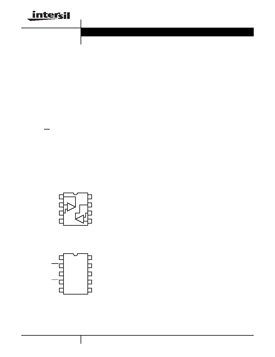
Pinouts
EL1516
(8-PIN SO, MSOP)
TOP VIEW
Features
· EL2227 upgrade replacement
· Voltage noise of only 1.3nV/
Hz
· Current noise of only 1.5pA/
Hz
· Bandwidth (-3dB) of 350MHz @ A
V
= -1
· Bandwidth (-3dB) of 250MHz @ A
V
= +2
· Gain-of-2 stable
· Just 5.5mA per amplifier
· 100mA I
OUT
· Fast enable/disable (EL1516A only)
· 5V to 12V operation
· Pb-free available (RoHS compliant)
Applications
· ADSL receivers
· VDSL receivers
· Home PNA receivers
· Ultrasound input amplifiers
· Wideband instrumentation
· Communications equipment
· AGC & PLL active filters
· Wideband sensors
VINB+
VINA-
VS-
ENA
VINA+
VOUTA
VS+
VINB-
VS-
VS+
VINA+
VINA-
VOUTA
VOUTB
VINB-
VINB+
1
2
3
4
8
7
6
5
-
+
-
+
ENB
VOUTB
EL1516A
(10-PIN MSOP)
TOP VIEW
1
2
3
4
10
9
8
7
5
6
Data Sheet
CAUTION: These devices are sensitive to electrostatic discharge; follow proper IC Handling Procedures.
1-888-INTERSIL or 321-724-7143
|
Intersil (and design) is a registered trademark of Intersil Americas Inc.
Copyright © Intersil Americas Inc. 2005. All Rights Reserved.
All other trademarks mentioned are the property of their respective owners.
May 4, 2005
2
FN7328.0
May 4, 2005
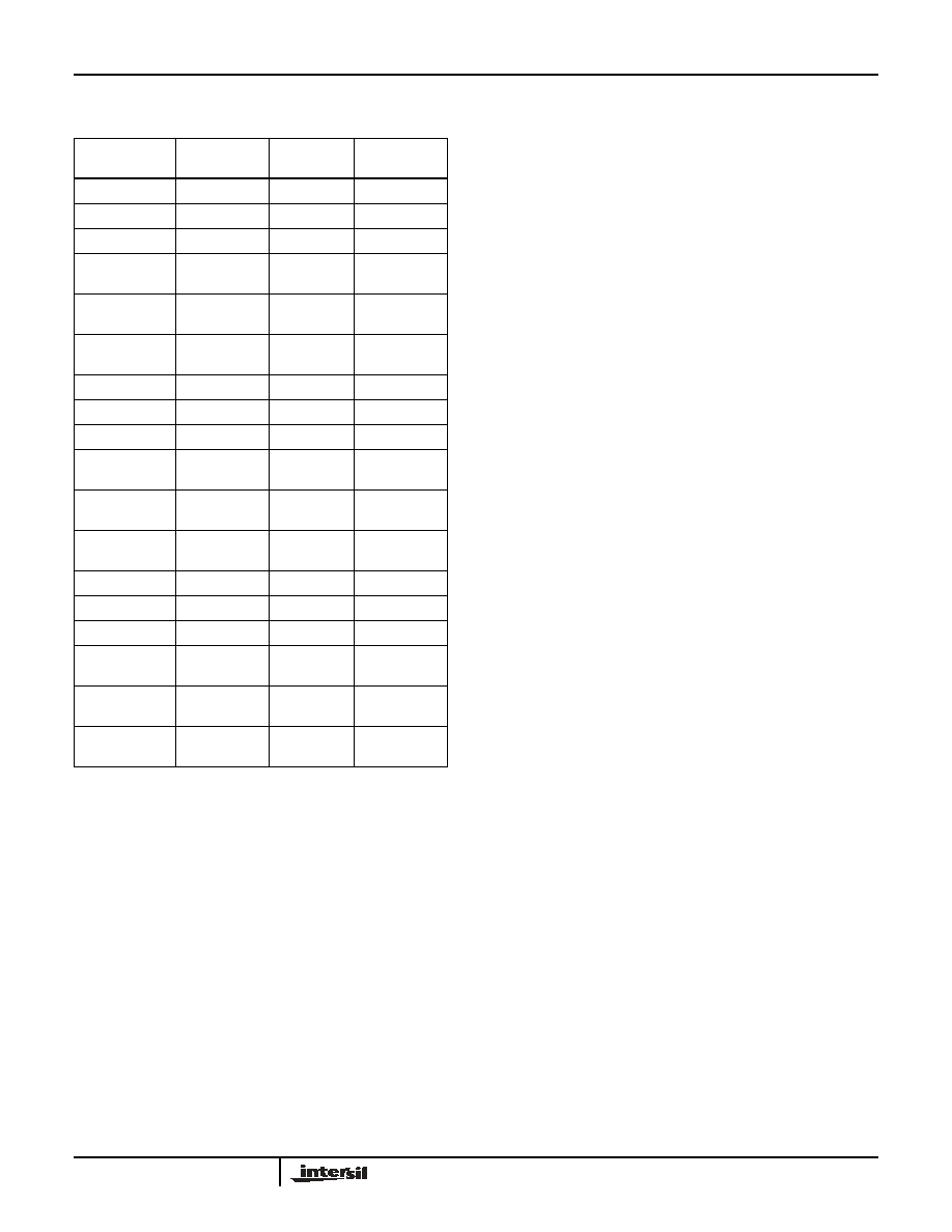
Ordering Information
PART
NUMBER
PACKAGE
TAPE &
REEL
PKG. DWG. #
EL1516IY
8-Pin MSOP
-
MDP0043
EL1516IY-T13
8-Pin MSOP
13"
MDP0043
EL1516IY-T7
8-Pin MSOP
7"
MDP0043
EL1516IYZ
(See Note)
8-Pin MSOP
(Pb-free)
-
MDP0043
EL1516IYZ-T13
(See Note)
8-Pin MSOP
(Pb-free)
13"
MDP0043
EL1516IYZ-T7
(See Note)
8-Pin MSOP
(Pb-free)
7"
MDP0043
EL1516IS
8-Pin SO
-
MDP0027
EL1516IS-T13
8-Pin SO
13"
MDP0027
EL1516IS-T7
8-Pin SO
7"
MDP0027
EL1516ISZ
(See Note)
8-Pin SO
(Pb-free)
-
MDP0027
EL1516ISZ-T13
(See Note)
8-Pin SO
(Pb-free)
13"
MDP0027
EL1516ISZ-T7
(See Note)
8-Pin SO
(Pb-free)
7"
MDP0027
EL1516AIY
10-Pin MSOP
-
MDP0043
EL1516AIY-T13
10-Pin MSOP
13"
MDP0043
EL1516AIY-T7
10-Pin MSOP
7"
MDP0043
EL1516AIYZ
(See Note)
10-Pin MSOP
(Pb-free)
-
MDP0043
EL1516AIYZ-
T13 (See Note)
10-Pin MSOP
(Pb-free)
13"
MDP0043
EL1516AIYZ-T7
(See Note)
10-Pin MSOP
(Pb-free)
7"
MDP0043
NOTE: Intersil Pb-free products employ special Pb-free material sets;
molding compounds/die attach materials and 100% matte tin plate
termination finish, which are RoHS compliant and compatible with
both SnPb and Pb-free soldering operations. Intersil Pb-free products
are MSL classified at Pb-free peak reflow temperatures that meet or
exceed the Pb-free requirements of IPC/JEDEC J STD-020.
EL1516, EL1516A
3
FN7328.0
May 4, 2005
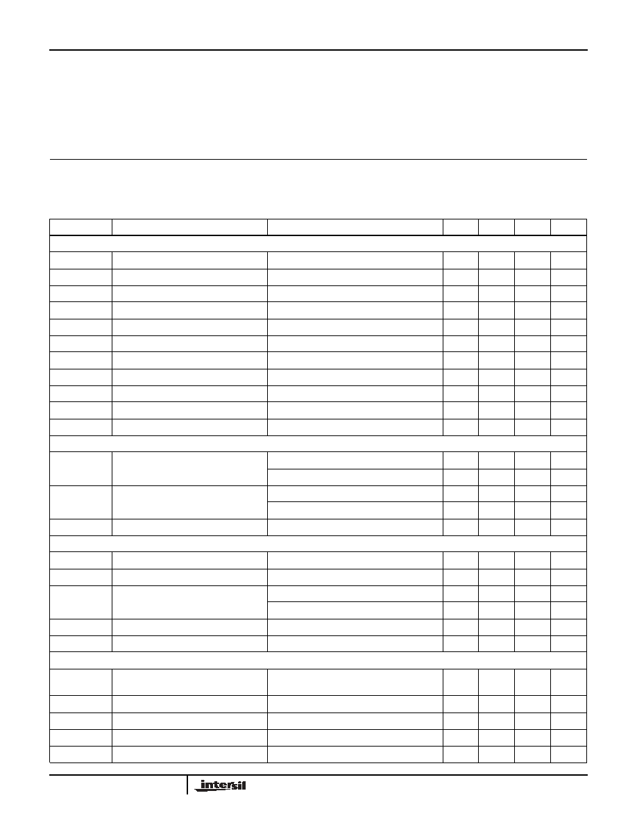
IMPORTANT NOTE: All parameters having Min/Max specifications are guaranteed. Typ values are for information purposes only. Unless otherwise noted, all tests are
at the specified temperature and are pulsed tests, therefore: T
J
= T
C
= T
A
Absolute Maximum Ratings
(T
A
= 25°C)
Supply Voltage between V
S
+ and V
S
- . . . . . . . . . . . . . . . . . . . . .14V
Input Voltage . . . . . . . . . . . . . . . . . . . . . . . . . . . V
S
- -0.3V, V
S
+0.3V
Maximum Continuous Output Current . . . . . . . . . . . . . . . . . . . 40mA
Maximum Die Temperature . . . . . . . . . . . . . . . . . . . . . . . . . . . 150°C
Storage Temperature . . . . . . . . . . . . . . . . . . . . . . . .-65°C to +150°C
Operating Temperature . . . . . . . . . . . . . . . . . . . . . . .-40°C to +85°C
Power Dissipation . . . . . . . . . . . . . . . . . . . . . . . . . . . . . See Curves
CAUTION: Stresses above those listed in "Absolute Maximum Ratings" may cause permanent damage to the device. This is a stress only rating and operation of the
device at these or any other conditions above those indicated in the operational sections of this specification is not implied.
Electrical Specifications
V
S
+
= +2.5V, V
S
-
= -2.5V, R
L
= 500
and C
L
= 3pF to 0V, R
F
= R
G
= 620
, V
CM
= 0V, and T
A
= 25°C, unless
otherwise specified.
PARAMETER
DESCRIPTION
CONDITIONS
MIN
TYP
MAX
UNIT
INPUT CHARACTERISTICS
V
OS
Input Offset Voltage
V
CM
= 0V
-0.2
+3
mV
TCV
OS
Average Offset Voltage Drift
-0.3
µV/°C
I
B
Input Bias Current
V
CM
= 0V
6.5
9
µA
I
OS
Input Offset Current
50
500
nA
R
IN
Input Impedance
2
M
C
IN
Input Capacitance
1.6
pF
CMIR
Common-Mode Input Range
-1.3
+1.7
V
CMRR
Common-Mode Rejection Ratio
for V
IN
from -4.7V to 5.4V
85
105
dB
A
VOL
Open-Loop Gain
V
O
= ±1.25V
70
75
dB
e
n
Voltage Noise
f = 100kHz
1.24
nV/
Hz
i
n
Current Noise
f = 100kHz
1.5
pA/
Hz
OUTPUT CHARACTERISTICS
V
OL
Output Swing Low
R
L
= 500
1.45
1.35
V
R
L
= 150
1.37
1.25
V
V
OH
Output Swing High
R
L
= 500
1.5
1.6
V
R
L
= 150
1.4
1.5
V
I
SC
Short Circuit Current
R
L
= 10
60
75
mA
POWER SUPPLY PERFORMANCE
PSRR
Power Supply Rejection Ratio
V
S
is moved from ±5.4V to ±6.6V
75
80
dB
I
S ON
Supply Current Enable (Per Amplifier)
No load
5.7
7
mA
I
S OFF
Supply Current Disable (Per Amplifier)
(EL1516A)
I+ (DIS)
2
5
µA
I- (DIS)
-19
-16
µA
TC I
S
I
S
Temperature Coefficient
32
µA/°C
V
S
Operating Range
5
12
V
DYNAMIC PERFORMANCE
SR
Slew Rate
V
O
= ±1.25V square wave, measured 25%-
75%
80
110
V/µs
TC SR
SR Temperature Coefficient
0.5
V/µs/°C
t
S
Settling to 0.1% (A
V
= +2)
A
V
= +2, V
O =
±1V
25
ns
BW1
-3dB Bandwidth
A
V
= -1, R
F =
100
320
MHz
BW2
-3dB Bandwidth
A
V
= +2, R
F =
100
200
MHz
EL1516, EL1516A
4
FN7328.0
May 4, 2005
HD2
2nd Harmonic Distortion
f = 1MHz, V
O
= 2V
P-P
, R
L
= 100
90
dBc
HD3
3rd Harmonic Distortion
f = 1MHz, V
O
= 2V
P-P
, R
L
= 100
95
dBc
ENABLE (EL1516AIY ONLY)
t
EN
Enable Time
125
ns
t
DIS
Disable Time
336
ns
I
IHEN
EN Pin Input High Current
EN = V
S
+
18
µA
I
ILEN
EN Pin Input Low Current
EN = V
S
-
10
nA
V
IHEN
EN Pin Input High Voltage for Power-
down
V
S
+ -1
V
V
IHEN
EN Pin Input Low Voltage for Power-up
V
S
- +3
V
Electrical Specifications
V
S
+
= +2.5V, V
S
-
= -2.5V, R
L
= 500
and C
L
= 3pF to 0V, R
F
= R
G
= 620
, V
CM
= 0V, and T
A
= 25°C, unless
otherwise specified.
(Continued)
PARAMETER
DESCRIPTION
CONDITIONS
MIN
TYP
MAX
UNIT
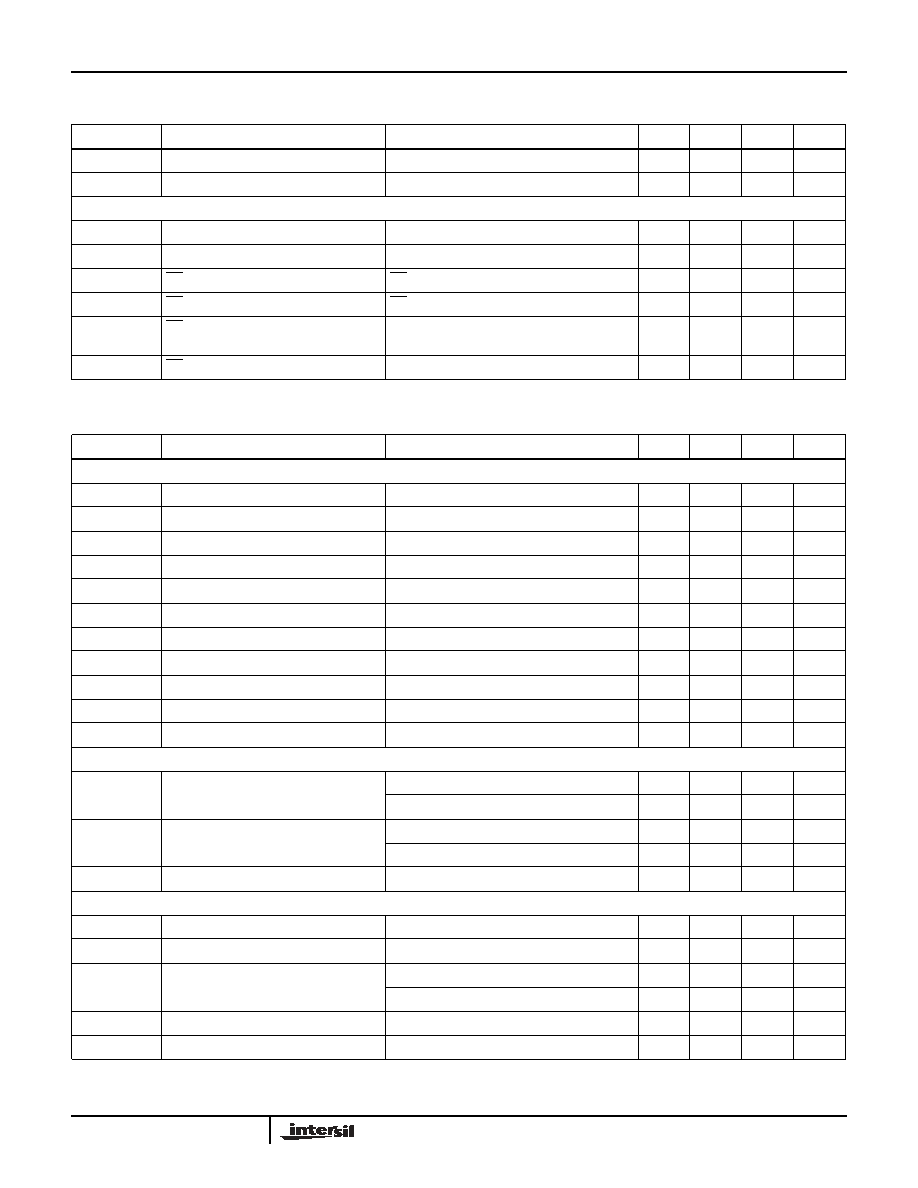
Electrical Specifications
V
S
+
= +6V, V
S
-
= -6V, R
L
= 500
and C
L
= 3pF to 0V, R
F
= R
G
= 620
, V
CM
= 0V, and T
A
= 25°C, unless
otherwise specified.
PARAMETER
DESCRIPTION
CONDITIONS
MIN
TYP
MAX
UNIT
INPUT CHARACTERISTICS
V
OS
Input Offset Voltage
V
CM
= 0V
0.1
3
mV
TCV
OS
Average Offset Voltage Drift
-0.3
µV/°C
I
B
Input Bias Current
V
CM
= 0V
6.5
9
µA
I
OS
Input Offset Current
50
500
nA
R
IN
Input Impedance
12
M
C
IN
Input Capacitance
1.6
pF
CMIR
Common-Mode Input Range
-4.5
+5.5
V
CMRR
Common-Mode Rejection Ratio
for V
IN
from -4.7V to 5.4V
90
110
dB
A
VOL
Open-Loop Gain
V
O
= ±2.5V
75
80
dB
e
n
Voltage Noise
f = 100kHz
1.24
nV/
Hz
i
n
Current Noise
f = 100kHz
1.5
pA/
Hz
OUTPUT CHARACTERISTICS
V
OL
Output Swing Low
R
L
= 500
-4.8
-4.7
V
R
L
= 150
-4.6
-4.5
V
V
OH
Output Swing High
R
L
= 500
4.8
4.9
V
R
L
= 150
4.5
4.7
V
I
SC
Short Circuit Current
R
L
= 10
110
160
mA
POWER SUPPLY PERFORMANCE
PSRR
Power Supply Rejection Ratio
V
S
is moved from ±5.4V to ±6.6V
75
85
dB
I
S ON
Supply Current Enable (Per Amplifier)
No load
5.8
7
mA
I
S OFF
Supply Current Disable (Per Amplifier)
(EL1516A)
I+ (DIS)
2
5
µA
I- (DIS)
-19
-16
µA
TC I
S
I
S
Temperature Coefficient
32
µA/°C
V
S
Operating Range
5
12
V
EL1516, EL1516A
5
FN7328.0
May 4, 2005
DYNAMIC PERFORMANCE
SR
Slew Rate
V
O
= ±2.5V square wave, measured 25%-75%
90
128
V/µs
TC SR
SR Temperature Coefficient
0.5
V/µs/°C
t
S
Settling to 0.1% (A
V
= +2)
A
V
= +2, V
O =
±1V
20
ns
BW1
-3dB Bandwidth
A
V
= -1, R
F =
100
350
MHz
BW2
-3dB Bandwidth
A
V
= +2, R
F =
100
250
MHz
HD2
2nd Harmonic Distortion
f = 1MHz, V
O
= 2V
P-P
, R
L
= 500
125
dBc
f = 1MHz, V
O
= 2V
P-P
, R
L
= 150
117
dBc
HD3
3rd Harmonic Distortion
f = 1MHz, V
O
= 2V
P-P
, R
L
= 500
115
dBc
f = 1MHz, V
O
= 2V
P-P
, R
L
= 150
110
dBc
ENABLE (EL1516AIY ONLY)
t
EN
Enable Time
125
ns
t
DIS
Disable Time
336
ns
I
IHEN
EN Pin Input High Current
EN = V
S
+
17
20
µA
I
ILEN
EN Pin Input Low Current
EN = V
S
-
7
20
nA
V
IHEN
EN Pin Input High Voltage for Power-
down
V
S
+ -1
V
V
IHEN
EN Pin Input Low Voltage for Power-up
V
S
- +3
V
Electrical Specifications
V
S
+
= +6V, V
S
-
= -6V, R
L
= 500
and C
L
= 3pF to 0V, R
F
= R
G
= 620
, V
CM
= 0V, and T
A
= 25°C, unless
otherwise specified.
(Continued)
PARAMETER
DESCRIPTION
CONDITIONS
MIN
TYP
MAX
UNIT
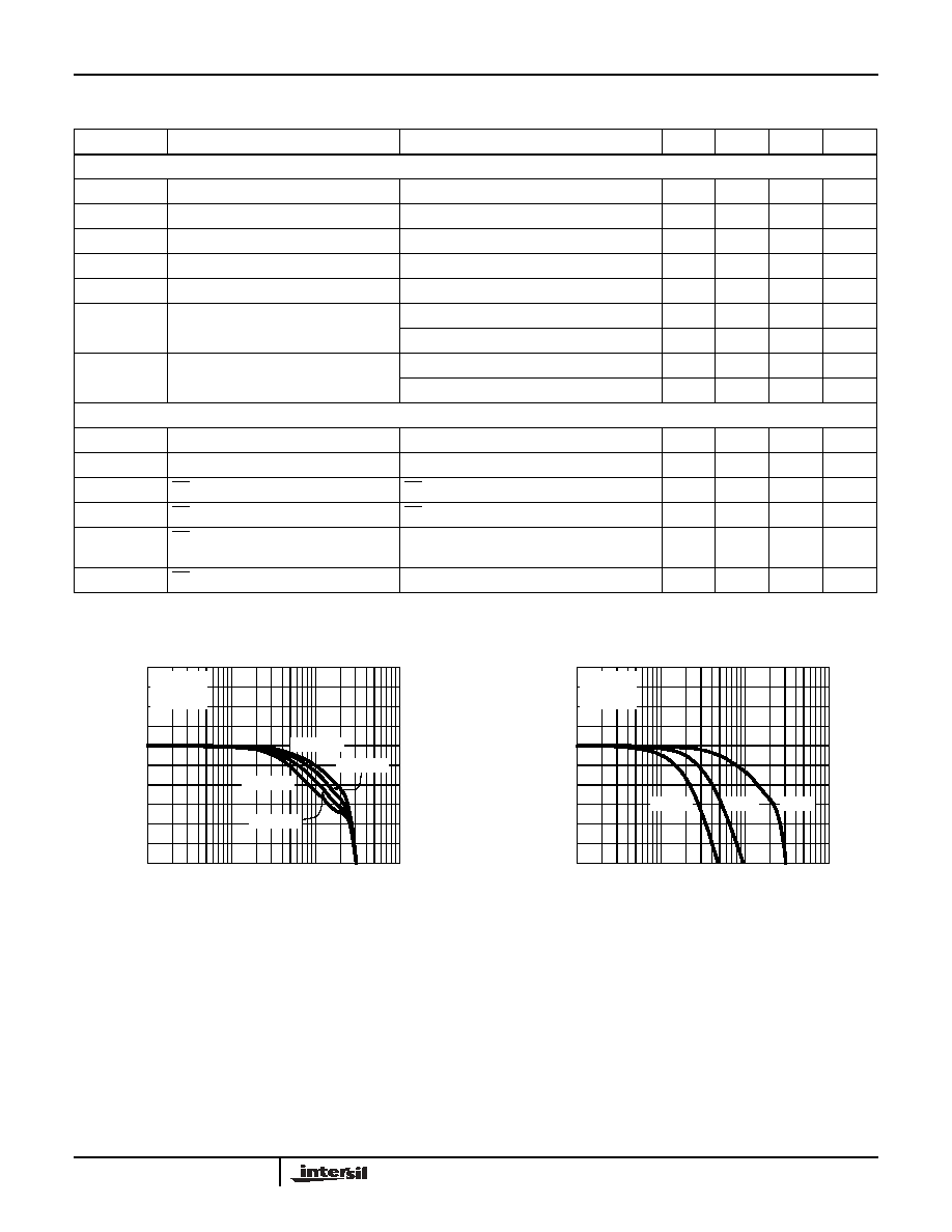
Typical Performance Curves
FIGURE 1. NON-INVERTING FREQUENCY RESPONSE FOR
VARIOUS R
F
FIGURE 2. NON-INVERTING FREQUENCY RESPONSE (GAIN)
1M
1G
10M
4
2
-6
FREQUENCY (Hz)
NORMALIZED GAIN
(dB)
100M
-4
V
S
=±6V
A
V
=+2
R
L
=500
0
-2
R
F
=100
R
F
=1k
R
F
=348
R
F
=619
V
S
=±6V
R
F
=348
R
L
=500
A
V
=10
A
V
=5
A
V
=2
1M
1G
10M
4
2
-6
FREQUENCY (Hz)
NORMALIZED GAIN
(dB)
100M
-4
0
-2
EL1516, EL1516A