 | –≠–ª–µ–∫—Ç—Ä–æ–Ω–Ω—ã–π –∫–æ–º–ø–æ–Ω–µ–Ω—Ç: EL2003CM | –°–∫–∞—á–∞—Ç—å:  PDF PDF  ZIP ZIP |
1
Æ
FN7022
CAUTION: These devices are sensitive to electrostatic discharge; follow proper IC Handling Procedures.
1-888-INTERSIL or 321-724-7143
|
Intersil (and design) is a registered trademark of Intersil Americas Inc.
Copyright © Intersil Americas Inc. 2003. All Rights Reserved. Elantec is a registered trademark of Elantec Semiconductor, Inc.
All other trademarks mentioned are the property of their respective owners.
EL2003, EL2033
100MHz Video Line Driver
The EL2003 and EL2033 are general
purpose monolithic unity gain buffers
featuring 100MHz, -3dB bandwidth
and 4ns small signal rise time. These buffers are capable of
delivering a ±100mA current to a resistive load and are
oscillation free into capacitive loads. In addition, the EL2003
and EL2033 have internal output short circuit current limiting
which will protect the devices under both a DC fault condition
and AC operation with reactive loads. The extremely fast
slew rate of 1200V/µs, wide bandwidth, and high output drive
make the EL2003 and EL2033 ideal choices for closed loop
buffer applications with wide band op amps. These same
characteristics and excellent DC performance make the
EL2003 and EL2033 excellent choices for open loop
applications such as driving coaxial and twisted pair cables.
The EL2003 and EL2033 are constructed using Elantec's
proprietary dielectric isolation process that produces PNP
and NPN transistors with essentially identical AC and DC
characteristics.
Features
∑ Differential gain 0.1%
∑ Differential phase 0.1∞
∑ 100mA continuous output current guaranteed
∑ Short circuit protected
∑ Wide bandwidth - 100MHz
∑ High slew rate - 1200V/µs
∑ High input impedance - 2M
∑ Low quiescent current drain
Applications
∑ Co-ax cable driver
∑ Flash converter driver
∑ Video DAC buffer
∑ Op amp booster
Ordering Information
PART
NUMBER
PACKAGE
TAPE & REEL
PKG. NO.
EL2003CN
8-Pin PDIP
-
MDP0031
EL2003CM
20-Pin SOL
-
MDP0027
EL2033CN
8-Pin PDIP
-
MDP0031
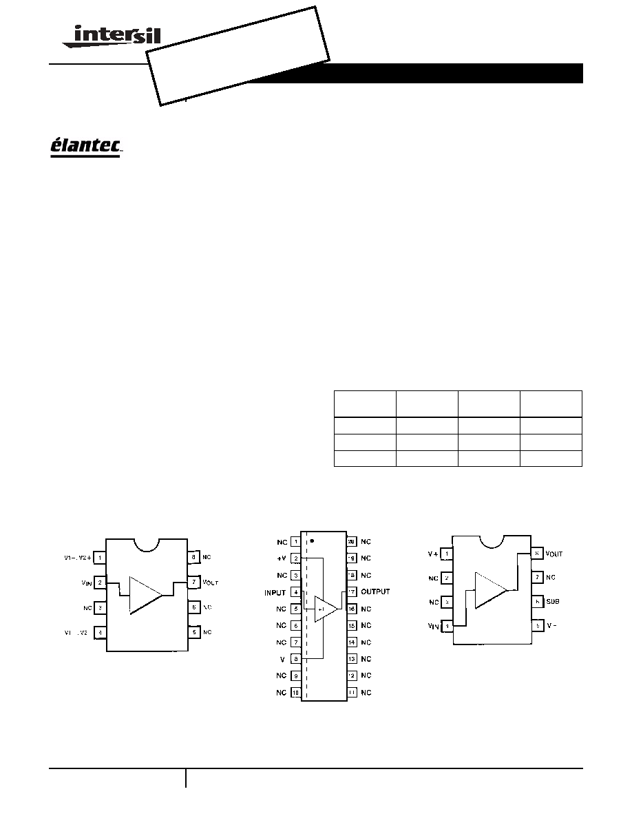
Pinouts
EL2003
(8-PIN PDIP)
TOP VIEW
EL2003
(20-PIN SOL)
TOP VIEW
EL2033
(8-PIN PDIP)
TOP VIEW
Data Sheet
September 1998, Rev. F
OBSO
LETE
PRO
DUCT
NO R
ECOM
MEND
ED R
EPLA
CEME
NT
conta
ct ou
r Tec
hnica
l Sup
port C
enter
at
1-888
-INTE
RSIL
or ww
w.inte
rsil.c
om/ts
c

2
Absolute Maximum Ratings
(T
A
= 25∞C)
V
S
Supply Voltage (V+ - V-) . . . . . . . . . . . . . . . . . . . ±18V or 36V
V
IN
Input Voltage . . . . . . . . . . . . . . . . . . . . . . . . . . . .±15V or V
S
If the input exceeds the ratings shown (or the supplies) or if the input to output
voltage exceeds ±7.5V then the input current must be limited to ±50 mA. See
the application hints for more information.
I
IN
Input Current (See note above) . . . . . . . . . . . . . . . . . ±50mA
P
D
Power Dissipation . . . . . . . . . . . . . . . . . . . . . . . See Curves
The maximum power dissipation depends on package type, ambient
temperature and heat sinking. See the characteristic curves for more details.
Output Short Circuit Duration . . . . . . . . . . . . . . . . . . . . . Continuous
A heat sink is required to keep the junction temperature below the absolute
maximum when the output is short circuited.
T
A
Operating Temperature Range
EL2003C/EL2033C. . . . . . . . . . . . . . . . . . . . . . -40∞C to +85∞C
T
J
Operating Junction Temperature
Metal Can . . . . . . . . . . . . . . . . . . . . . . . . . . . . . . . . . . . 175∞C
Plastic . . . . . . . . . . . . . . . . . . . . . . . . . . . . . . . . . . . . . . 150∞C
T
ST
Storage Temperature . . . . . . . . . . . . . . . . . . . -65∞C to +150∞C
CAUTION: Stresses above those listed in "Absolute Maximum Ratings" may cause permanent damage to the device. This is a stress only rating and operation of the
device at these or any other conditions above those indicated in the operational sections of this specification is not implied.
IMPORTANT NOTE: All parameters having Min/Max specifications are guaranteed. Typical values are for information purposes only. Unless otherwise noted, all tests
are at the specified temperature and are pulsed tests, therefore: T
J
= T
C
= T
A
Electrical Specifications
V
S
= ±15V, R
S
= 50
PARAMETER
DESCRIPTION
TEST CONDITIONS
LIMITS
UNIT
V
IN
LOAD
TEMP
MIN
TYP
MAX
V
OS
Output Offset Voltage
0
25∞C
-40
5
40
mV
T
MIN
, T
MAX
-50
50
mV
I
IN
Input Current
0
25∞C, T
MAX
-25
-5
25
µA
T
MIN
-50
50
µA
R
IN
Input Resistance
±12V
100
25∞C, T
MAX
0.5
2
M
T
MIN
0.05
M
A
V1
Voltage Gain
±12V
1k
25∞C
0.98
0.99
V/V
T
MIN
, T
MAX
0.97
V/V
A
V2
Voltage Gain
±6V
50
25∞C
0.83
0.90
V/V
T
MIN
, T
MAX
0.80
V/V
A
V3
Voltage Gain with V
S
= ±5V
±3V
50
25∞C
0.82
0.89
V/V
T
MIN
, T
MAX
0.79
V/V
V
01
Output Voltage Swing
±14V
1k
25∞C
±13
±13.5
V
T
MIN
, T
MAX
±12.5
V
V
02
Output Voltage Swing
±12V
100
25∞C
±10.5
±11.3
V
T
MIN
, T
MAX
±10
V
R
OUT
Output Resistance
±2V
50
25∞C
7
10
T
MIN
, T
MAX
12
I
OUT
Output Current
±12V
(Note 1)
25∞C
±105
±230
mA
T
MIN
, T
MAX
±100
mA
I
S
Supply Current
0
25∞C, T
MAX
10
15
mA
T
MIN
20
mA
PSRR
Supply Rejection (Note 2)
0
25∞C
60
80
dB
T
MIN
, T
MAX
50
dB
SR1
Slew Rate (Note 3)
±10V
1k
25∞C
600
1200
V/µs
SR2
Slew Rate (Note 4)
±5V
50
25∞C
200
400
V/µs
THD
Distortion @ 1kHz
4V
RMS
50
25∞C
0.2
1
%
EL2003, EL2033
3
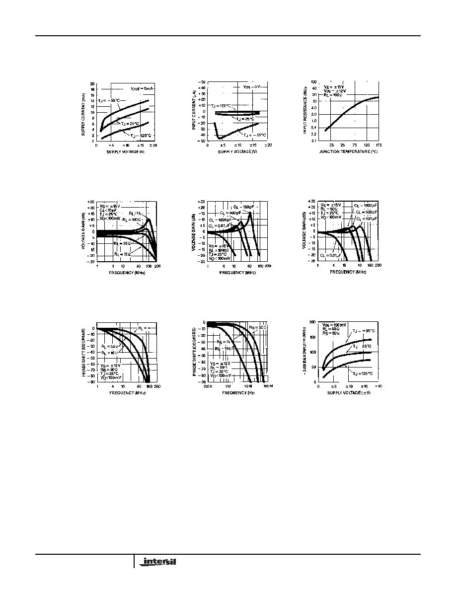
Typical Performance Curves
Quiescent Supply Current
vs Supply Voltage
Input Current
vs Supply Voltage
Input Resistance
vs Temperature
Voltage Gain vs Frequency
Various Resistive Loads
Voltage Gain vs Frequency
No Resistive Load
Various Capacitive Loads
Voltage Gain vs Frequency
50
Resistive Load
Various Capacitive Loads
Phase Shift vs Frequency
Various Resistive Loads
Phase Shift vs Frequency
Various Source Resistors
-3dB Bandwidth
vs Supply Voltage
EL2003, EL2033
4
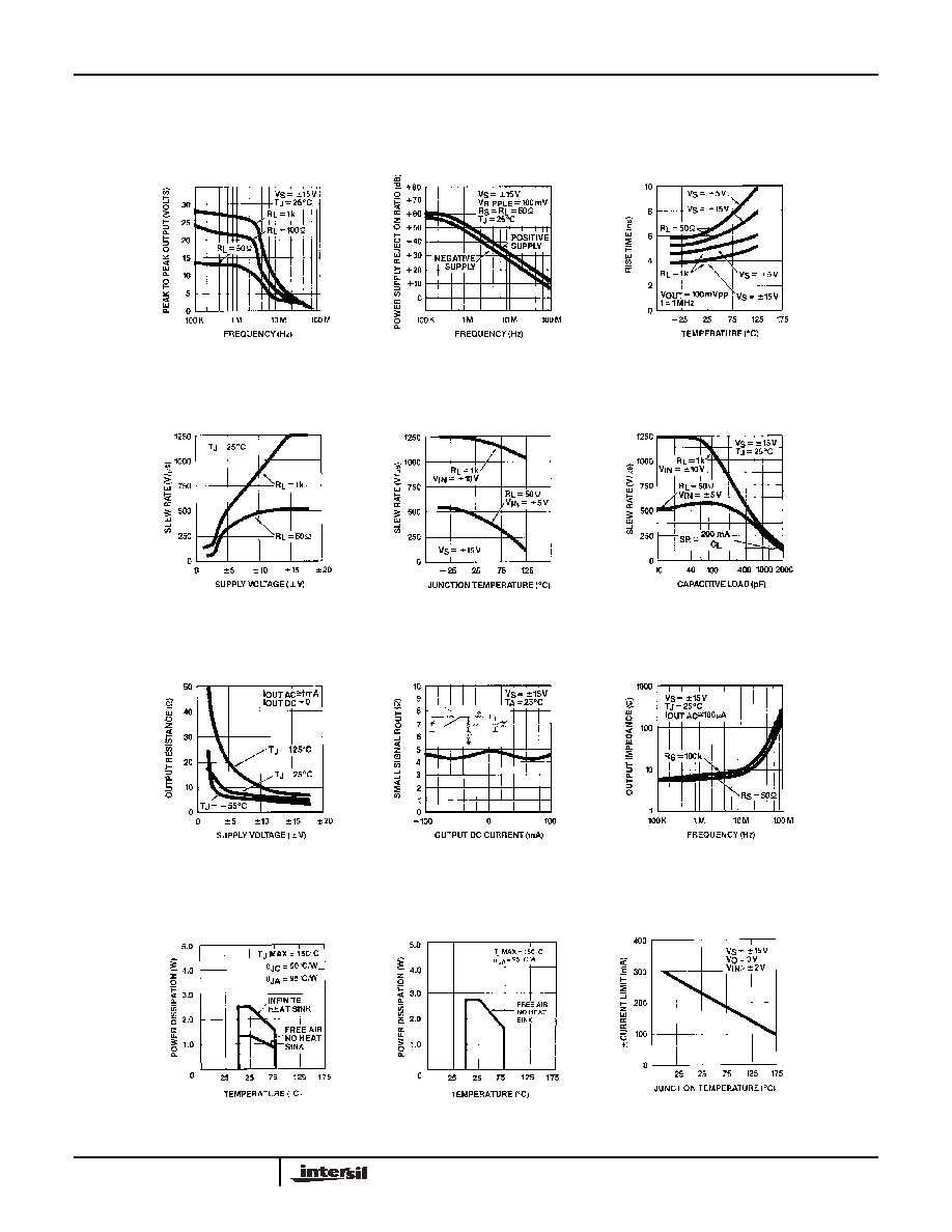
Typical Performance Curves
(Continued)
Maximum Undistorted
Output Voltage
vs Frequency
Power Supply Rejection
Ratio vs Frequency
Rise Time
vs Temperature
Slew Rate
vs Supply Voltage
Slew Rate
vs Temperature
Slew Rate
vs Capacitive Load
Output Resistance
vs Supply Voltage
Small Signal
Output Resistance
vs DC Output Current
Output Impedance
vs Frequency
8-Pin Plastic DIP
Maximum Power
Dissipation
vs Ambient Temperature
20-Pin SOL
Maximum Power
Dissipation
vs Ambient Temperature
Current Limit
vs Temperature
EL2003, EL2033

5
Applications Information
The EL2003 and EL2033 are monolithic buffer amplifiers
built with Elantec's proprietary dielectric isolation process
that produces NPN and PNP complimentary transistors. The
circuits are connection of symmetrical common collector
transistors that provide both sink and source current
capability independent of output voltage while maintaining
constant output and input impedances. The high slew rate
and wide bandwidth of the EL2003 and EL2033 make them
useful beyond video frequencies.
Power Supplies
The EL2003 and EL2033 may be operated with single or
split supplies as low as ±2.5V (5V total) to as high as ±18V
(36V total). However, the bandwidth, slew rate, and output
impedance degrade significantly for supply voltages less
than ±5V (10V total) as shown in the characteristic curves. It
is not necessary to use equal value split supplies, for
example -5V and +12V would be excellent for 0V to 1V video
signals.
Bypass capacitors from each supply pin to a ground plane
are recommended. The EL2003 and EL2033 will not
oscillate even with minimal bypassing, however, the supply
will ring excessively with inadequate capacitance. To
eliminate a supply ringing and the interference it can cause,
a 10µF tantalum capacitor with short pins is recommended
for both supplies. Inadequate supply bypassing can also
result in lower slew rates and longer settling times.
Input Range
The input to the EL2003 and EL2033 looks like a high
resistance in parallel with a few picofarads in addition to a
DC bias current. The input characteristics change very little
with output loading, even when the amplifier is in current
limit. However, there are clamp diodes from the input to the
output that protect the transistor base emitter junctions.
These diodes start to conduct at about ±9.5V input to output
differential voltage. Of course the input resistance drops
dramatically when the diodes start conducting; the diodes
are rated at ±50mA.
The input characteristics also change when the input voltage
exceeds either supply by 0.5V. This happens because the
input transistor's base-collector junctions forward bias. If the
input exceeds the supply by LESS than 0.5V and then
returns to the normal input range, the output will recover in
less than 10ns. However, if the input exceeds the supply by
MORE than 0.5V, the recovery time can be hundreds of
nanoseconds. For this reason it is recommended that
schottky diode clamps from input to supply be used if a fast
recovery from large input overloads is required.
Source Impedance
The EL2003 and EL2033 have excellent input-output
isolation and are very tolerant of variations in source
impedances. Capacitive sources cause no problems at all,
resistive sources up to 100k
present no problems as long
as care is used in board layout to minimize output to input
coupling. Inductive sources can cause oscillations; a 1k
resistor in series with the buffer input pin will usually
eliminate problems without sacrificing too much speed. An
unterminated cable or other resonant source can also cause
oscillations. Again, an isolating resistor will eliminate the
problem.
Current Limit
The EL2003 and EL2033 have internal current limits that
protect the output transistors. The current limit goes down
with junction temperature rise as shown in the characteristic
curves. At a junction temperature of +175∞C the current
limits are at about 100mA. If the EL2003 or EL2033 output is
shorted to ground when operating on ±15V supplies, the
power dissipation will be greater than 1.5W. A heat sink is
required in order for the EL2003 or EL2033 to survive an
indefinite short. Recovery time to come out of current limit is
about 250ns.
Heat Sinking
When operating the EL2003 and EL2033 in elevated
ambient temperatures and/or high supply voltages and low
impedance loads, the internal power dissipation can force
the junction temperature above the maximum rating (150∞C
for the plastic DIP). Also, an indefinite short of the output to
ground will cause excessive power dissipation.
The thermal resistance junction to case is 50∞C/W for the
plastic DIP. A suitable heat sink will increase the power
dissipation capability significantly beyond that of the package
alone. Several companies make standard heat sinks for both
packages. Aavid and Thermalloy heat sinks have been used
successfully.
Parallel Operation
If more than 100mA output is required or if heat
management is a problem, several EL2003 or EL2033s may
be paralleled together. The result is as though each device
was driving only part of the load. For example, if two units
are paralleled then a 50
load looks like 100
to each
EL2003. Parallel operation results in lower input and output
impedances, increased bias current but no increase in offset
voltage. An example showing three EL2003s in parallel and
also the addition of a FET input buffer stage is shown below.
By using a dual FET the circuit complexity is minimal and the
performance is excellent. Take care to minimize the stray
capacitance at the input of the EL2003s for maximum slew
rate and bandwidth.
EL2003, EL2033