 | –≠–Ľ–Ķ–ļ—ā—Ä–ĺ–Ĺ–Ĺ—č–Ļ –ļ–ĺ–ľ–Ņ–ĺ–Ĺ–Ķ–Ĺ—ā: EL2021 | –°–ļ–į—á–į—ā—Ć:  PDF PDF  ZIP ZIP |
1
ģ
FN7027
CAUTION: These devices are sensitive to electrostatic discharge; follow proper IC Handling Procedures.
1-888-INTERSIL or 321-724-7143
|
Intersil (and design) is a registered trademark of Intersil Americas Inc.
Copyright © Intersil Americas Inc. 2003. All Rights Reserved. Elantec is a registered trademark of Elantec Semiconductor, Inc.
All other trademarks mentioned are the property of their respective owners.
EL2021
Monolithic Pin Driver
The EL2021 is designed to drive
programmed voltages into difficult
loads. It has the required circuitry to be
used as the pin driver electronics in board test systems.
Capable of overpowering logic outputs, the part can
accurately drive independently set high and low levels with
programmed Slew Rates into reactive loads. It can also be
placed into high impedance to monitor the load without
having to disconnect. Previous board testers had
multiplexing schemes to reduce the number of pin drivers
required. With the small size and power consumption of the
monolithic EL2021, a driver per node with little or no
multiplexing becomes practical. Since only a few pins of
"bed-of-nails" board testers need be active at any given time,
the power-down feature saves substantial power in large
systems.
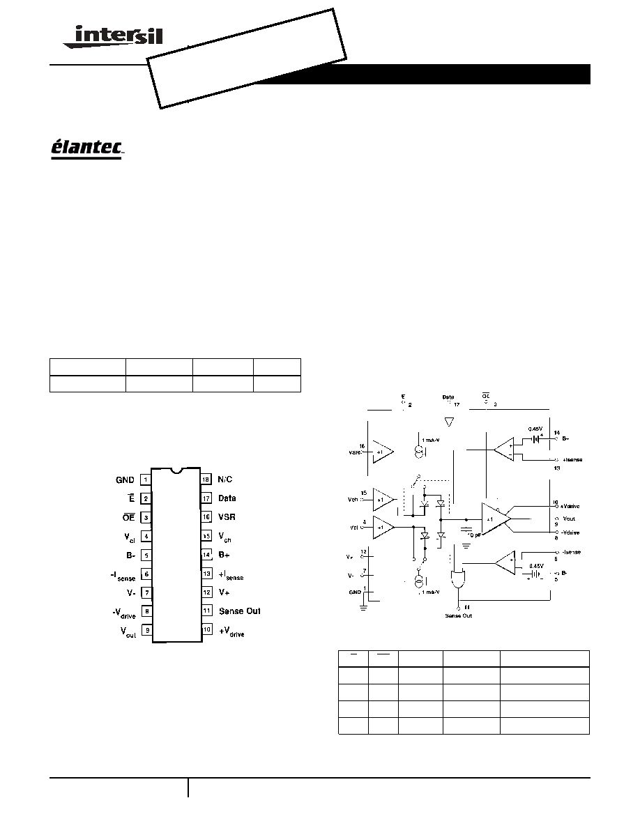
Pinout
EL2021
(18-PIN DIP)
TOP VIEW
Features
∑ Wide range of programmable analog output levels
∑ 0.5 Ampere output drive with external transistors
∑ Programmable Slew Rate
∑ Low overshoot with large capacitive loads-stable with
500pF
∑ 3-state output
∑ Power-down capability
∑ Wide supply range
∑ Overcurrent sense
Applications
∑ Loaded circuit board testers
∑ Digital testers
∑ Programmable 4-quadrant power supplies
Block Diagram
Ordering Information
PART NUMBER
TEMP. RANGE
PACKAGE
PKG. NO.
EL2021CJ
0įC to +75įC
CerDIP
MDP0031
Truth Table
E
OE
DATA
V
OUT
COMMENTS
0
0
0
V
CL
Active
0
0
1
V
CH
Active
0
1
X
High-Z
Third State
1
X
X
Undefined
Power-down
Data Sheet
November 1993, Rev. F
OBS
OLE
TE P
ROD
UCT
NO R
ECO
MME
NDE
D RE
PLA
CEM
ENT
cont
act o
ur Te
chni
cal S
uppo
rt Ce
nter
at
1-88
8-INT
ERS
IL or
www
.inte
rsil.c
om/t
sc

2
Absolute Maximum Ratings
(T
A
= 25įC)
V+
Supply Voltage . . . . . . . . . . . . . . . . . . . . . -0.3V to +16V
V-
Supply Voltage . . . . . . . . . . . . . . . . . . . . . 0.03V to -16V
B+, B-
Supply Voltages . . . . . . . . . . . . . . . . . . . . . . . . V- to V+
Sense+
Input Voltages. . . . . . . . . . . . . (-2V + B+) to (0.3V +B+)
Sense-
Input Voltages. . . . . . . . . . . . . . (-0.3V + B-) to (2V + B-)
E, VSR,
OE, Data
Input Voltages. . . . . . . . . . . . . . . . . . . . . . . . -0.3 to +6V
V
CH
, V
CL
Input Voltages . . . . . . . . . . . . . . . . B- to B+ and V- to V+
Sense Out
Output Current. . . . . . . . . . . . . . . . . . -10mA to +10mA
V
OUT
, Drive+,
Drive-
Output Currents. . . . . . . . . . . . . . . . . . . . -45mA to +45mA
T
J
Junction Temperature . . . . . . . . . . . . . . . . . . . . . . . . 150įC
T
A
Operating Ambient
Temperature Range. . . . . . . . . . . . . . . . . . . . 0įC to +75įC
T
ST
Storage Temperature. . . . . . . . . . . . . . . . . -65įC to +150įC
P
D
Power Dissipation (T
A
= 25įC)
(See Curves) . . . . . . . . . . . . . . . . . . . . . . . . . . . . . . . . 1.8W
CAUTION: Stresses above those listed in "Absolute Maximum Ratings" may cause permanent damage to the device. This is a stress only rating and operation of the
device at these or any other conditions above those indicated in the operational sections of this specification is not implied.
IMPORTANT NOTE: All parameters having Min/Max specifications are guaranteed. Typical values are for information purposes only. Unless otherwise noted, all tests
are at the specified temperature and are pulsed tests, therefore: T
J
= T
C
= T
A
DC Electrical Specifications
T
A
= 25įC, V+ = 15, V- = -10V, B+ = V
CH
+3.6V, B- = V
CL
-3.6V, No Load. Data and OE levels are:
L = 2.0V and H = 3.0V (CMOS thresholds). E levels are: L = 1.5V and H = 3.5V. All tests done using
2N2222 and 2N2907 output transistors with Beta>40 @ I
C
= 400mA and Beta>27 @ I
C
= 500mA and
V
CE
= 3.1V. OE and E low.
PARAMETER
DESCRIPTION
CONDITIONS
MIN
TYP
MAX
UNITS
I
S
V+, -Supply Currents
V
CH
= 5V, V
CL
= 0, VSR = 2.5V, Data = H or L
V
CH
= 11V, V
CL
= -6V, VSR = 5V, Data = H or L
V
CH
= -6V, V
CL
= 11V, VSR+2.5V, Data = H or L
15
21
15
25
33
25
30
45
30
mA
mA
mA
I
S
, disabled
V+, -Supply Currents
V
CH
= 5V, V
CL
= 0V, VSR = 2.5V, Data = H or L, E = H
0
0.5
2.5
mA
I
VCH
V
CH
Input Current
V
CH
= -1V to +7.5V, V
CL
= 0V, VSR = 5V,
Data = H or L
-20
5
20
ĶA
I
VCL
V
CL
Input Current
V
CL
= -3.5V to +3.5V, V
CH
= 0V, VSR = 5V,
Data = H or L
-20
-5
20
ĶA
I
DATA
Data Input Current
V
CH
= 5V, V
CL
= 0V, VSR = 5V, Data = 0 or 5V
-50
5
50
ĶA
I
OE
OE Input Current
V
CH
= 5V, V
CL
= 0V, VSR = 5V, Data = L, OE = 0V or 5V
-20
5
20
ĶA
I
E
E Input Current
V
CH
= 5V, V
CL
= 0V, VSR = 5V, Data = L, E = 0V or 5V
-20
2
20
ĶA
I
VSR
VSR Input Current
V
CH
= 5V, V
CL
= 0V, Data = L, VSR = 0V or 5V
-20
2
20
ĶA
ĪI
SENSE
Sense Input Currents
V
CH
= 5V, V
CL
= 0V, VSR = 5V, Data = 0V or 5V
-20
5
20
ĶA
I
B
+, I
B
-
B+, B- Input Currents
V
CH
= 5V, V
CL
= 0V, Data = L, VSR = 5V
-20
5
20
ĶA
V
O
Output Voltage
V+ = 14.5V, V- = -9.5V
V
CH
= 5V, V
CL
= 0, VSR = 1V, Data = L,
Output Current = -100mA, 0mA, or +100mA
Output Current = -400mA or +400mA
Output Current = -500mA or +500mA
V
CH
= 5V, V
CL
= 0, VSR = 1V, Data = H
Output Current = -100mA, 0mA, or +100mA
Output Current = -400mA or +400mA
Output Current = -500mA or +500mA
V
CH
= 11V, V
CL
= -6V, VSR = 1V, I
OUT
= 0, Data = L
V
CH
= 11V, V
CL
= -6V, VSR = 1V, I
OUT
= 0, Data = H
-50
-300
-600
4.95
4.7
4.4
-6.1
10.9
50
300
600
5.05
5.3
5.6
-5.9
11.1
mV
mV
mV
V
V
V
V
V
I
SENSE+
I
SENSE-
+ISENSE
Threshold
-ISENSE
Threshold
V
CH
= 5V, V
CL
= 0, VSR = 2.5V, R
SENSE
= 1
, Data = H
V
CH
= 5V, V
CL
= 0, VSR = 2.5V, R
SENSE
= 1
, Data = L
400
-400
450
-450
600
-600
mA
mA
V
O, SENSE
Sense Out Levels
V
CH
= 5V, V
CL
= 0, VSR = 2.5V, Data L or H,
Output Current = -350mA or +350mA
Output Current = -550mA or +550mA
0
3.5
0.6
5.0
V
V
I
OUT,TRI
High-Impedance
Output Leakage
V
CH
= 5V, V
CL
= 0, VSR = 2.5V, Data = L, OE = H,
Output Voltage = -2.5V or +7.5V
-100
5
100
ĶA
EL2021

3
AC Electrical Specifications
DC test conditions apply except where noted. For AC tests, R
L
= 1k, C
L
= 200pF. Delay times are
measured from OE or Data crossing 2.5V, V
CH
= 5V, V
CL
= 0.
PARAMETER
DESCRIPTION
CONDITIONS
MIN
TYP
MAX
UNITS
SR+
+Slew Rate
Data L to H, Output from 0.5V to 4.5V, VSR = 1V
VSR = 3V
80
150
100
240
120
360
V/Ķs
V/Ķs
SR-
-Slew Rate
Data H to L, Output from 4.5V to 0.5V, VSR = 1V
VSR = 3V
-80
-150
-100
-240
-120
-360
V/Ķs
V/Ķs
SRSYM
Slew Rate
Symmetry
-10
-20
10
20
%
%
T
PD
Propagation Delay
Data L to H, Output to 0.2V, VSR = 2.5V
Data H to L, Output to 4.8V, VSR = 2.5V
6.5
6.5
9
9
11.5
11.5
ns
ns
T
S
Settling Time
VSR = 5V, Data L to H, Output 4.5V to 5VĪ0.2V
VSR = 5V, Data H to L, Output 0.5V to Ī0.2V
30
30
ns
ns
OS
Overshoot
VSR = 1V, Data L to H or H to L
VSR = 1V, OE H to L, Data = L, R
L
to 5V
VSR = 1V, OE H to L, Data = H, R
L
to 0V
-300
-300
-300
300
300
300
mV
mV
mV
T
PDA
Propagation Delay,
High-Z to Active
VSR = 2.5V, OE H to L, C
L
= 50pF
R
L
to 5V, Data = L, Output to 3.5V
R
L
to 0V, Data = H, Output to 1.5V
50
50
ns
ns
T
PDH
Propagation Delay,
Active to High-Z
VSR = 2.5V, OE L to H, C
L
= 50pF,
Data = L, R
L
to 5V, Output to 0.5V
Data = H, R
L
to 0V, Output to 4.5V
50
50
ns
ns
Pin Description Table
PIN #
NAME
DESCRIPTION
1
GND
System ground.
2
E
Enable control input. A logic low allows normal operation; a logic high puts the device into
power down mode. No output levels are defined in powerdown nor does the output behave
as a high impedance.
3
OE
Output Enable input. A logic low sets the output to low-impedance driver mode; a logic high
places the output into a high-impedance state.
4
V
CL
Lower analog control input. When Data = OE = E = L, the V
CL
level is output as V
OUT
(assuming V
CL
< V
CH
).
5
B-
System power supply. The EL2021 uses this pin as a negative output current monitor connection.
Little current is drawn from this pin, transient or static.
6
I
SENSE
-
Negative output current monitor input.
7
V-
Negative power supply. Because all negative output drive currents come from this pin
(as much as 60mA transiently), good bypassing is essential.
8
Drive-
Output to external pnp transistor base.
9
V
OUT
High-current input and output, depending on OE.
10
Drive+
Output to external npn transistor base.
11
Sense Out
Logic output which signals that a high + or - output current is flowing.
12
V+
Positive power supply. Like V-, it should be well bypassed.
13
I
SENSE
+
Positive output current monitor input.
14
B+
System power supply, similar to B-.
15
V
CH
Higher analog control input. When Data = H and OE = E = L, the V
CH
level is output as
V
OUT
(assuming V
CH
> V
CL
).
16
VSR
Slew rate control input. A 1V level on this pin causes the output to slew at 100V/Ķs, 0.5V
causes a slew rate of 50V/Ķs, etc.
17
Data
Output level control input. This pin digitally selects V
CL
or V
CH
as the output voltage
when OE = E = L.
18
N/C
Not Connected.
SR+
(
)
- SR-
(
)
SR+
(
)
+ SR-
(
)
--------------------------------------
VSR
1V
=
VSR
2V
=
EL2021

4
Typical Performance Curves
Family of output waveshapes.
ECL, TTL, CMOS, HCMOS
with C1 = 50pF, VSR = 1V.
Family of output waveshapes.
ECL, TTL, CMOS, HCMOS
with C1 = 200pF, VSR = 1V.erting Gains
Output waveshapes with
5 MHz data rate. C1 = 50pF,
VSR = 4V.
Family of output waveshapes.
ECL, TTL, CMOS, HCMOS
with C1 = 200pF, VSR = 1V,
and overcompensated with
22pF from each drive pin
to ground.
Family of output waveshapes
from active H, L to
high-impedance H, L.
Family of output waveshapes
from high-impedance H, L
to active H, L.
Family of + output edges,
0V to 5V for VSR = 0.5V, 1V,
2V, 3V, 5V.
Family of--output edges,
5V to 0V or VSR = 0.5V, 1V,
2V, 3V, 5V.
EL2021

5
Typical Performance Curves
(Continued)
Applications Information
Output Stage
To meet the requirements of low output impedance, wide
bandwidth, and large capacitive load driving capability, the
EL2021 has a fairly exotic output stage. Figure 1 shows a
simplified schematic of the circuit, only applicable in normal,
low impedance mode. External transistors are used to
handle the large load currents and peak power dissipations.
Since there is no need for good AC crossover distortion
performance in a pin driver, the output transistors are
operated class C. That is, for small output currents, neither
output transistor will conduct bias current, and when load
currents do flow, one of the devices is off. This is
accomplished by biasing the output transistors from Schottky
diodes D1 and D2. In operation, the diode forward voltage is
about 0.4V, whereas the "on" output transistor will have a
V
BE
of 0.6V. This leaves only 0.2V across the "off"
transistor's base-emitter junction, not nearly enough to
cause bias currents to flow in it. Schottky diodes have a
temperature drift similar to silicon transistors, so the class C
bias maintains over temperature. One caution is that the
diodes are in the IC package and are thermally separate
from the transistors, so there can exist temperature
differences between packages that can cause thermal
runaway. Runaway is avoided as long as the external
transistors are not hotter than the EL2021 package by more
than 80įC. The only way runaway has been induced as of
this writing is to use "freeze spray" on the IC package while
the output transistors are very hot.
Overshoot vs VSR
Overshoot vs VSR
Slew Rate vs VSR
Tri-State Leakage vs
Output Voltage
Supply Current vs
Supply Voltage
V
OUT
vs Load Current
Supply Current vs VSR
Power Dissipation vs
Temperature
EL2021