 | –≠–ª–µ–∫—Ç—Ä–æ–Ω–Ω—ã–π –∫–æ–º–ø–æ–Ω–µ–Ω—Ç: EL2070 | –°–∫–∞—á–∞—Ç—å:  PDF PDF  ZIP ZIP |
1
Æ
FN7031
CAUTION: These devices are sensitive to electrostatic discharge; follow proper IC Handling Procedures.
1-888-INTERSIL or 321-724-7143
|
Intersil (and design) is a registered trademark of Intersil Americas Inc.
Copyright © Intersil Americas Inc. 2003. All Rights Reserved. Elantec is a registered trademark of Elantec Semiconductor, Inc.
All other trademarks mentioned are the property of their respective owners.
EL2070
200MHz Current Feedback Amplifier
The EL2070 is a wide bandwidth, fast
settling monolithic amplifier
incorporating a disable/enable feature.
Built using an advanced complementary bipolar process, this
amplifier uses current-mode feedback to achieve more
bandwidth at a given gain than conventional operational
amplifiers. Designed for closed-loop gains of ±1 to ±8, the
EL2070 has a 200MHz -3dB bandwidth (A
V
= +2), and 12ns
settling to 0.05% while consuming only 15mA of supply
current. Furthermore, the fast disable/enable times of
200ns/100ns allow rapid analog multiplexing.
The EL2070 is an obvious high-performance solution for
video distribution and line-driving applications, especially
when its disable feature can be used for fast analog
multiplexing. Furthermore, the low 15mA supply current, and
the very low 5mA of supply current when disabled suggest
use in systems where power is critical. With differential
gain/phase of 0.02%/0.01∞, guaranteed video specifications,
and a minimum 50mA output drive, performance in these
areas is assured.
The EL2070's settling to 0.05% in 12ns, low distortion, and
ability to drive capacitive loads make it an ideal flash A/D
driver. The wide 200MHz bandwidth and extremely linear
phase allow unmatched signal fidelity. D/A systems can also
benefit from the EL2070, especially if linearity and drive
levels are important.
Features
∑ 200MHz -3dB bandwidth, A
V
= 2
∑ Disable/enable
∑ 12ns settling to 0.05%
∑ V
S
= ±5V @ 15mA
∑ Low distortion: HD2, HD3 @-60dBc at 20MHz
∑ Differential gain 0.02% at NTSC, PAL
∑ Differential phase 0.01∞ at NTSC, PAL
∑ Overload/short-circuit protected
∑ ±1 to ±8 closed-loop gain range
∑ Low cost
Applications
∑ Video gain block
∑ Video distribution
∑ HDTV amplifier
∑ Analog multiplexing (using disable)
∑ Power-down mode (using disable)
∑ High-speed A/D conversion
∑ D/A I-V conversion
∑ Photodiode, CCD preamps
∑ IF processors
∑ High-speed communications
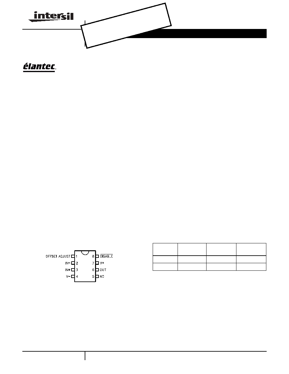
Pinout
EL2070
(8-PIN SO, PDIP)
TOP VIEW
Manufactured under U.S. Patent No. 4,893,091
Ordering Information
PART
NUMBER
TEMP.
RANGE
PACKAGE
PKG. NO.
EL2070CN
-40∞C to +85∞C
8-Pin PDIP
MDP0031
EL2070CS
-40∞C to +85∞C
8-Pin SO
MDP0027
Data Sheet
September 26, 2001
OBS
OLE
TE P
ROD
UCT
NO R
ECO
MME
NDE
D RE
PLA
CEM
ENT
cont
act o
ur Te
chni
cal S
uppo
rt Ce
nter
at
1-88
8-INT
ERS
IL or
www
.inte
rsil.c
om/t
sc
2
Absolute Maximum Ratings
(T
A
= 25∞C)
Supply Voltage (V
S
) . . . . . . . . . . . . . . . . . . . . . . . . . . . . . . . . . . .±7V
Output Current . . . . . . . . . . . . . . . . . . . . . . . . . . . . . . . . . . . . . 70mA
(Output is short-circuit protected to ground, however, maximum reliability is
obtained if I
OUT
does not exceed 70mA)
Common-Mode Input Voltage . . . . . . . . . . . . . . . . . . . . . . . . . . ±V
S
Differential Input Voltage . . . . . . . . . . . . . . . . . . . . . . . . . . . . . . . .5V
Disable Input Voltage . . . . . . . . . . . . . . . . . . . . . . . . . . . . . . +V
S
, -1V
Thermal Resistance
. . . . . . . . . . . . . . . . . . . . . . . . .
JA
= 95∞C/W PDIP
. . . . . . . . . . . . . . . . . . . . . . . . . . . . . . . . . . . . . . . .
JA
= 175∞C/W SO-8
Applied Output Voltage (Disabled). . . . . . . . . . . . . . . . . . . . . . . .±V
S
Power Dissipation . . . . . . . . . . . . . . . . . . . . . . . . . . . . . See Curves
Operating Temperature . . . . . . . . . . . . . . . . . . . . . . . . -40C to +85C
Pin Temperature (Soldering, 5 Seconds). . . . . . . . . . . . . . . . . 300∞C
Junction Temperature . . . . . . . . . . . . . . . . . . . . . . . . . . . . . . . 175∞C
Storage Temperature . . . . . . . . . . . . . . . . . . . . . . . . -60∞C to +150∞C
CAUTION: Stresses above those listed in "Absolute Maximum Ratings" may cause permanent damage to the device. This is a stress only rating and operation of the
device at these or any other conditions above those indicated in the operational sections of this specification is not implied.
IMPORTANT NOTE: All parameters having Min/Max specifications are guaranteed. Typical values are for information purposes only. Unless otherwise noted, all tests
are at the specified temperature and are pulsed tests, therefore: T
J
= T
C
= T
A
Open-Loop DC Electrical Specifications
V
S
= ±5V, R
L
= 100
unless otherwise specified
PARAMETER
DESCRIPTION
TEST
CONDITIONS
TEMP
MIN
TYP
MAX
UNIT
V
OS
Input Offset Voltage
25∞C
2
5.5
mV
T
MIN
8.2
mV
T
MAX
9.0
mV
d(V
OS
)/dT
Average Offset
Voltage Drift
(Note 1)
All
10.0
40.0
µV/∞C
+I
IN
+Input Current
25∞C, T
MAX
10
25.0
µA
T
MIN
36.0
µA
d(+I
IN
)/dT
Average +Input
Current Drift
(Note 1)
All
50.0
200.0
nA/∞C
-I
IN
-Input Current
25.0∞C
10
30
µA
T
MIN
, T
MAX
46
µA
d(-I
IN
)/dT
Average -Input
Current Drift
(Note 1)
All
50.0
200.0
nA/∞C
PSRR
Power Supply
Rejection Ratio
All
45.0
50.0
dB
CMRR
Common-Mode
Rejection Ratio
All
40.0
50.0
dB
I
S
Supply Current--Quiescent
No Load
All
16.0
20.0
mA
IS
OFF
Supply Current--Disabled
(Note 2)
All
4.0
7.0
mA
+R
IN
+Input Resistance
25∞C, T
MAX
100.0
200.0
k
T
MIN
50.0
k
C
IN
Input Capacitance
All
0.5
2.0
pF
R
OUT
Output Impedance (DC)
All
0.1
0.2
R
OUT
D
Output Resistance (DC)
Disabled
All
100.0
200.0
k
C
OUT
D
Output Capacitance (DC)
Disabled
All
0.5
2.0
pF
CMIR
Common-Mode
Input Range
(Note 3)
25∞C, T
MAX
2.0
2.1
V
T
MIN
1.2
V
I
OUT
Output Current
25∞C, T
MAX
50.0
70.0
mA
T
MIN
35.0
mA
V
OUT
Output Voltage Swing
No Load
All
3.3
3.5
V
EL2070
3
V
OUT
L
Output Voltage Swing
100
25∞C
3.0
3.4
V
-ICMR
Input Current Common
Mode Rejection
25∞C
8.0
33.0
µA/V
+IPSR
+Input Current Power
Supply Rejection
25∞C
1.0
3.6
µA/V
-IPSR
-Input Current Power
Supply Rejection
25∞C
20
24
µA/V
R
OL
Transimpedance
25∞C
30.0
125.0
V/mA
T
MIN
80.0
V/mA
T
MAX
140.0
V/mA
I
LOGIC
Pin 8 Current @ 0V
All
0.8
1.2
mA
V
DIS
Maximum Pin 8
V to Disable
All
0.5
V
V
EN
Minimum Pin 8
V to Enable
All
3.5
V
I
DIS
Minimum Pin 8
I to Disable
All
350.0
µA
I
EN
Maximum Pin 8
I to Enable
All
60.0
µA
NOTES:
1. Measured from T
MIN
to T
MAX
.
2. Supply current when disabled is measured at the negative supply.
3. Common-mode input range for rated performance.
Open-Loop DC Electrical Specifications
V
S
= ±5V, R
L
= 100
unless otherwise specified (Continued)
PARAMETER
DESCRIPTION
TEST
CONDITIONS
TEMP
MIN
TYP
MAX
UNIT
Closed-Loop AC Electrical Specifications
V
S
= ±5V, R
F
= 250
, A
V
= +2, R
L
= 100
unless otherwise specified
PARAMETER
DESCRIPTION
TEST CONDITIONS
TEMP
MIN
TYP
MAX
UNIT
FREQUENCY RESPONSE
SSBW
-3dB Bandwidth
(V
OUT
< 0.5V
PP
)
25∞C
150.0
200.0
MHz
T
MIN
150.0
MHz
T
MAX
120.0
MHz
LSBW
-3dB Bandwidth
(V
OUT
< 5.0V
PP
)
A
V
= +5
All
35.0
50.0
MHz
GAIN FLATNESS
GFPL
Peaking
V
OUT
< 0.5V
PP
< 40MHz
25∞C
0.0
0.3
dB
T
MIN
, T
MAX
0.4
dB
GFPH
Peaking
V
OUT
< 0.5V
PP
> 40MHz
25∞C
0.0
0.5
dB
T
MIN
, T
MAX
0.7
dB
GFR
Rolloff
V
OUT
< 0.5V
PP
< 75MHz
25∞C
0.6
1.0
dB
T
MIN
1.0
dB
T
MAX
1.3
dB
LPD
Linear Phase Deviation
V
OUT
< 0.5V
PP
< 75MHz
25∞C, T
MIN
0.2
1.0
∞
T
MAX
1.2
∞
EL2070
4
NOTES:
1. Noise Tests are performed from 5MHz to 200MHz.
2. Differential gain/phase tests are with R
L
= 100
.
For other values of R
L
, see curves.
TIME-DOMAIN RESPONSE
t
R1
, t
F1
Rise Time, Fall Time
0.5V Step
All
1.6
2.4
ns
t
R2
, t
F2
Rise Time, Fall Time
5.0V Step
All
6.5
10.0
ns
t
S1
Settling Time to 0.1%
2.0V Step
All
10.0
13.0
ns
t
S2
Settling Time to 0.05%
2.0V Step
All
12.0
15.0
ns
OS
Overshoot
0.5V Step
25∞C, T
MAX
0.0
10.0
%
T
MIN
15.0
%
SR
Slew Rate
A
V
= +2
All
430.0
700.0
V/µs
A
V
= - 2
All
1600.0
V/µs
DISTORTION
HD2
2nd Harmonic Distortion
at 20MHz
2V
PP
25∞C
-60.0
-45.0
dBc
T
MIN
-40.0
dBc
T
MAX
-45.0
dBc
HD3
3rd Harmonic Distortion
at 20MHz
2V
PP
25∞C
-60.0
-50.0
dBc
T
MIN
, T
MAX
-50.0
dBc
EQUIVALENT INPUT NOISE
NF
Noise Floor
> 100kHz
(Note 1)
25∞C
-157.0
-154.0
dBm (1Hz)
T
MIN
-154.0
dBm (1Hz)
T
MAX
-153.0IV
dBm (1Hz)
INV
Integrated Noise
100kHz to 200MHz
(Note 1)
25∞C
40.0
57.0
µV
T
MIN
57.0
µV
T
MAX
63.0
µV
DISABLE/ENABLE PERFORMANCE
T
OFF
Disable Time to > 50dB
10MHz
All
1000.0
IV
ns
T
ON
Enable Time
All
200.0
ns
OFFIso
Off Isolation
10MHz
All
55.0
59.0
dB
VIDEO PERFORMANCE
d
G
Differential Gain (Note 2)
NTSC/PAL
25∞C
0.02
0.08
% pp
d
P
Differential Phase (Note 2)
NTSC/PAL
25∞C
0.01
0.08
∞ pp
d
G
Differential Gain (Note 2)
30MHz
25∞C
0.05
0.18
% pp
d
P
Differential Phase (Note 2)
30MHz
25∞C
0.05
0.18
∞ pp
VBW
-0.1dB Bandwidth (Note 2)
25∞C
30.0
60.0
MHz
Closed-Loop AC Electrical Specifications
V
S
= ±5V, R
F
= 250
, A
V
= +2, R
L
= 100
unless otherwise specified (Continued)
PARAMETER
DESCRIPTION
TEST CONDITIONS
TEMP
MIN
TYP
MAX
UNIT
EL2070
5
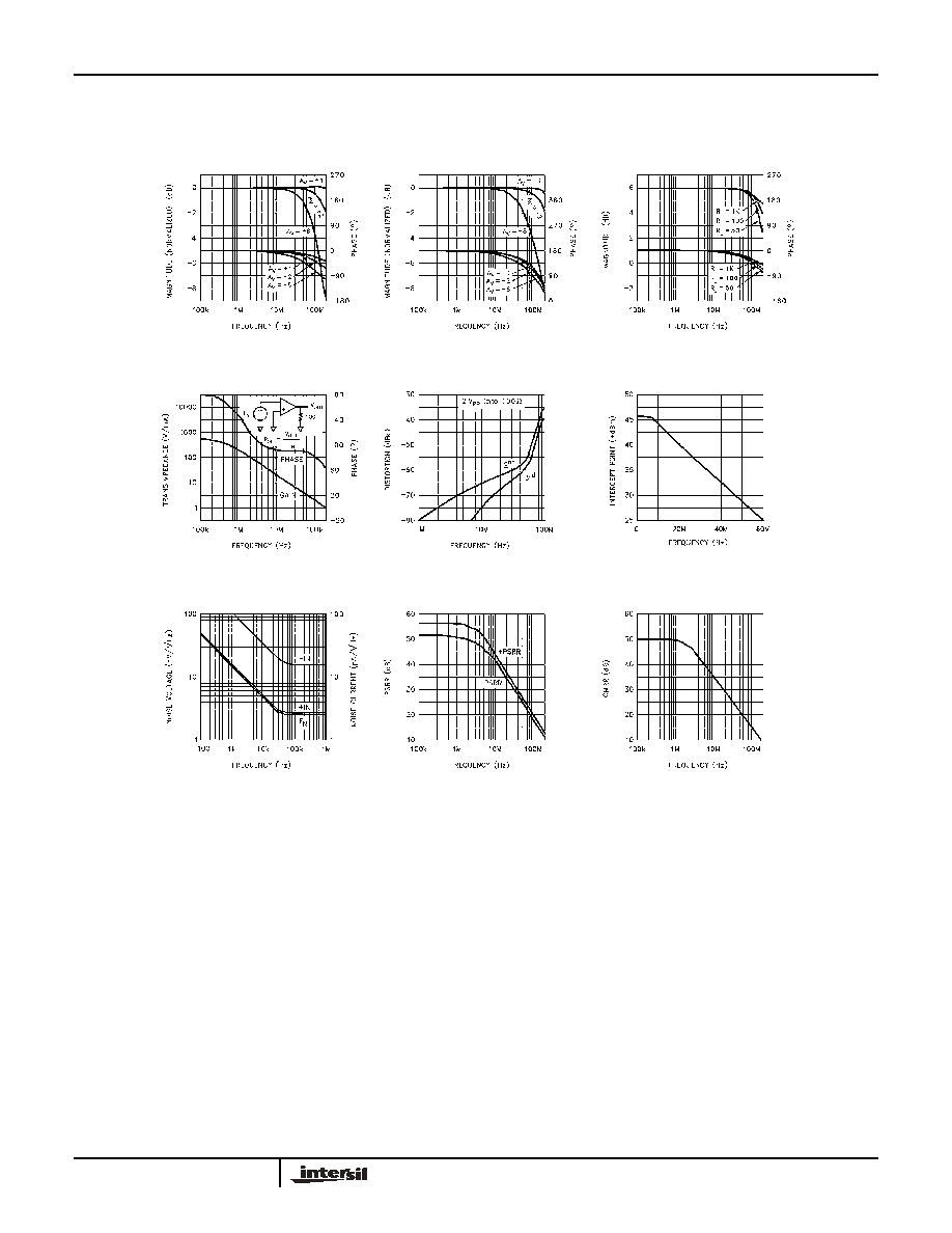
Typical Performance Curves
Non-Inverting
Frequency Response
Inverting
Frequency Response
Frequency Response for
Various R
L
s
2-Tone 3rd Order
Intermodulation Intercept
2nd and 3rd
Harmonic Distortion
Open-Loop Transimpedance
Gain and Phase
Equivalent Input Noise
Power-Supply
Rejection Ratio
Common-Mode
Rejection Ratio
EL2070