 | –≠–ª–µ–∫—Ç—Ä–æ–Ω–Ω—ã–π –∫–æ–º–ø–æ–Ω–µ–Ω—Ç: EL2090CM | –°–∫–∞—á–∞—Ç—å:  PDF PDF  ZIP ZIP |
1
Æ
FN7040
CAUTION: These devices are sensitive to electrostatic discharge; follow proper IC Handling Procedures.
1-888-INTERSIL or 321-724-7143
|
Intersil (and design) is a registered trademark of Intersil Americas Inc.
Copyright © Intersil Americas Inc. 2003. All Rights Reserved. Elantec is a registered trademark of Elantec Semiconductor, Inc.
All other trademarks mentioned are the property of their respective owners.
EL2090
100MHz DC-Restored Video Amplifier
The EL2090 is the first complete DC-
restored monolithic video amplifier
sub-system. It contains a very high-
quality video amplifier and a nulling sample-and-hold
amplifier specifically designed to stabilize video
performance. When the HOLD logic input is set to a logic 0
during a horizontal sync, the sample-and-hold amplifier may
be used as a general-purpose op-amp to null the DC offset
of the video amplifier. When the HOLD input goes to a logic
1 the sample-and-hold stores the correction voltage on the
hold capacitor to maintain DC correction during the
subsequent scan line.
The video amplifier is optimized for video characteristics,
and performance at NTSC is nearly perfect. It is a current-
feedback amplifier, so that -3dB bandwidth changes little at
various closed-loop gains. The amplifier easily drives video
signal levels into 75
loads. With 100MHz bandwidth, the
EL2090 is also useful in HDTV applications.
The sample-and-hold is optimized for fast sync pulse
response. The application circuit shown will restore the video
DC level in five scan lines, even if the HOLD pulse is only
2µs long. The output impedance of the sample-and-hold is
low and constant over frequency and load current so that the
performance of the video amplifier is not compromised by
connections to the DC restore circuitry.
The EL2090 is fabricated in Elantec's proprietary
Complementary Bipolar process which produces NPN and
PNP transistors with equivalent AC and DC performance.
The EL2090 is specified for operation over the 0∞C to 75∞C
temperature range.
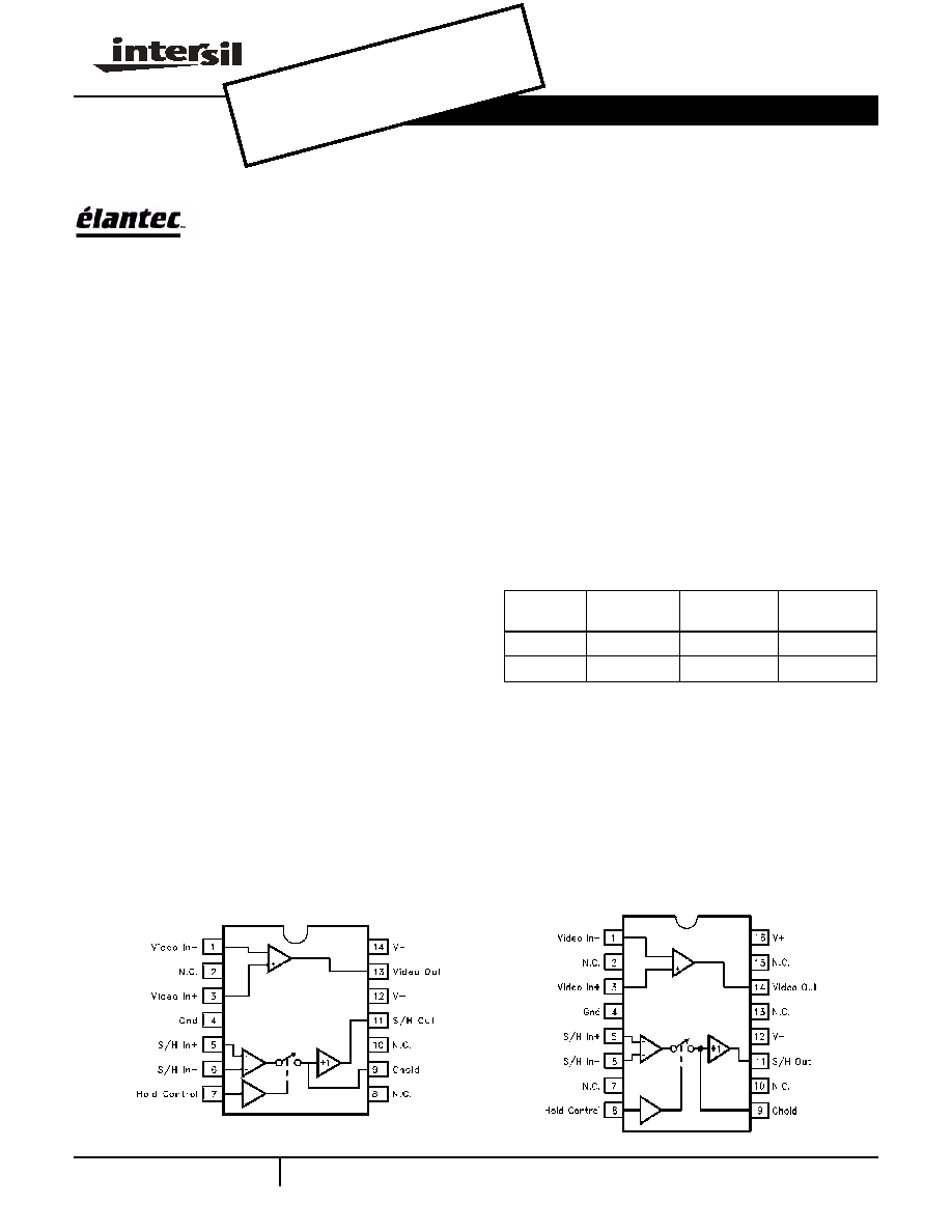
Pinouts
Features
∑ Complete video level restoration system
∑ 0.01% differential gain and 0.02∞ differential phase
accuracy at NTSC
∑ 100MHz bandwidth
∑ 0.1dB flatness to 20MHz
∑ Sample-and-hold has 15nA typical leakage and 1.5pC
charge injection
∑ System can acquire DC correction level in 10µs, or 5 scan
lines of 2µs each, to 1/2 IRE
∑ V
S
= ±5V to ±15V
∑ TTL/CMOS hold signal
Applications
∑ Input amplifier in video equipment
∑ Restoration amplifier in video mixers
EL2090
(14-PIN DIP)
TOP VIEW
EL2090
(16-PIN SOL)
TOP VIEW
Ordering Information
PART
NUMBER
TEMP.
RANGE
PACKAGE
PKG. NO.
EL2090CN
0∞C to +75∞C
14-Pin PDIP
MDP0031
EL2090CM
0∞C to +75∞C
16-Pin SOL
MDP0027
Data Sheet
August 1995, Rev. A
OBS
OLE
TE P
ROD
UCT
NO R
ECO
MME
NDE
D RE
PLAC
EME
NT
cont
act o
ur Te
chni
cal S
uppo
rt Ce
nter
at
1-88
8-INT
ERS
IL or
www
.inte
rsil.c
om/t
sc
2
Absolute Maximum Ratings
(T
A
= 25∞C)
Voltage between V+ and V- . . . . . . . . . . . . . . . . . . . . . . . . . . . . .36V
Voltage between V
IN
+, S/H
IN
+, S/H
IN
-, C
HOLD
,
and GND pins (V+) . . . . . . . . . . . . . . . . . . . . . . . +0.5V to (V-) -0.5V
V
OUT
Current. . . . . . . . . . . . . . . . . . . . . . . . . . . . . . . . . . . . . . 60mA
Current into V
IN
- and HOLD Pins . . . . . . . . . . . . . . . . . . . . . . . 5mA
Current S/H
OUT
. . . . . . . . . . . . . . . . . . . . . . . . . . . . . . . . . . . . 16mA
Internal Power Dissipation . . . . . . . . . . . . . . . . . . . . . . . See Curves
Operating Ambient Temperature Range . . . . . . . . . . . . 0∞C to 75∞C
Operating Junction Temperature Plastic DIP or SOL. . . . . . . . 150∞C
Storage Temperature Range . . . . . . . . . . . . . . . . . . -65∞C to +150∞C
CAUTION: Stresses above those listed in "Absolute Maximum Ratings" may cause permanent damage to the device. This is a stress only rating and operation of the
device at these or any other conditions above those indicated in the operational sections of this specification is not implied.
IMPORTANT NOTE: All parameters having Min/Max specifications are guaranteed. Typical values are for information purposes only. Unless otherwise noted, all tests
are at the specified temperature and are pulsed tests, therefore: T
J
= T
C
= T
A
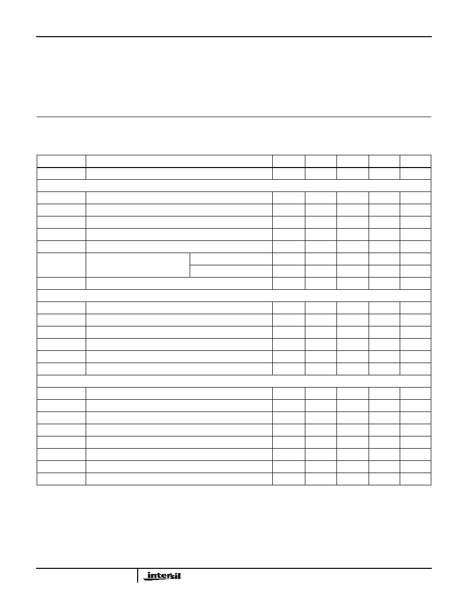
Open-Loop DC Electrical Specifications
V
S
= ±15V; R
L
= 150
, T
A
= 25∞C unless otherwise specified
PARAMETER
DESCRIPTION
TEMP
MIN
TYP
MAX
UNITS
I
S
Total Supply Current
Full
14
17
mA
VIDEO AMPLIFIER SECTION (NOT RESTORED)
V
OS
Input Offset Voltage
Full
8
70
mV
I
B+
+V
IN
Input Bias Current
Full
2
15
µA
I
B-
-V
IN
Input Bias Current
Full
30
150
µA
R
OL
Transimpedance
25∞C
300
V/mA
A
VOL
Open-Loop Voltage Gain; V
OUT
= ±2V
Full
56
65
dB
V
O
Output Voltage Swing
V
S
= ±15V; R
L
= 2k
Full
±12
±13
V
V
S
= ±5V; R
L
= 150
Full
±3.0
±3.5
V
I
SC
Short-Circuit Current; +V
IN
Set to ±2V; -V
IN
to Ground through 1k
25∞C
±50
±90
±160
mA
SAMPLE-AND-HOLD SECTION
V
OS
Input Offset Voltage
Full
2
10
mV
I
B
Input Bias Current
Full
0.5
2.5
µA
I
OS
Input Offset Current
Full
0.05
0.5
µA
R
IN, DIFF
Input Differential Resistance
25∞C
200
k
R
IN, COMM
Input Common-Mode Resistance
25∞C
100
M
V
CM
Common-Mode Input Range
Full
±11
±12.5
V
SAMPLE-AND-HOLD SECTION
A
VOL
Large Signal Voltage Gain
Full
15k
50k
V/V
CMRR
Common-Mode Rejection Ratio; V
CM
= ±11V
Full
75
95
dB
PSRR
Power-Supply Rejection Ratio; V
S
= ±5V to ±15V
Full
75
95
dB
V
THRESH
HOLD Pin Logic Threshold
Full
0.8
1.4
2.0
V
I
DROOP
Hold Mode Droop Current
Full
10
50
nA
I
CHARGE
Charge Current Available to Chold
Full
±90
±135
µA
V
O
Output Swing; R
L
= 2k
Full
±10
±13
V
I
SC
Short-Circuit Current
25∞C
±10
±17
±40
mA
EL2090
3
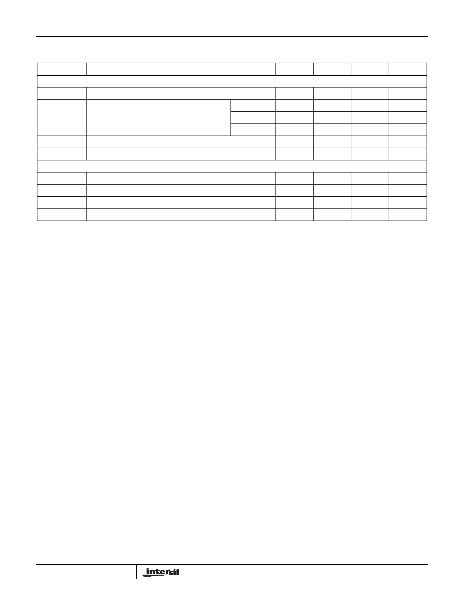
NOTE:
1. The logic input is between 0V and 5V, with a 220
resistor in series with the HOLD pin and 39pF capacitor from HOLD pin to ground.
Closed-Loop AC Electrical Specifications
V
S
= ±15V; C
L
= 15pF; C
STRAY
(-V
IN
) = 2.5pF; R
F
= R
G
= 300
; R
L
= 150
;
C
HOLD
= 100pF; T
A
= 25∞C
PARAMETER
DESCRIPTION
MIN
TYP
MAX
UNITS
VIDEO AMPLIFIER SECTION
SR
SlewRate; V
OUT
from -2 to +2V
600
V/µs
BW
Bandwidth;
-3dB
75
100
MHz
±1dB
35
60
MHz
±0.1dB
10
20
MHz
dG (Peaking)
Differential Gain; V
IN
from -0.7V to 0.7V; F = 3.58MHz
0.01
%
d
(Peaking)
Differential Phase; V
IN
from -0.7V to 0.7V; F = 3.58MHz
0.02
∞
SAMPLE-AND-HOLD SECTION
BW
Gain-Bandwidth Product
1.3
MHz
Q
Sample to Hold Charge Injection (Note 1)
1.5
5
pC
T
Sample to Hold or Hold to Sample Delay Time
20
ns
T
s
Sample to Hold Settling Time to 2mV
200
ns
EL2090
4
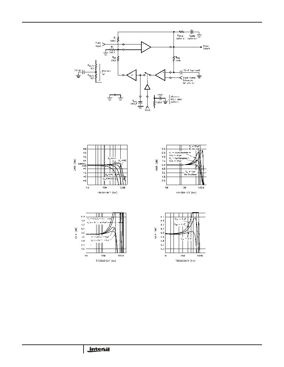
Typical Performance Curves
FIGURE 1. TYPICAL APPLICATION (A
V
= +2)
Relative Frequency Response
for Various Gains
Frequency Response with
Different Loads (A
V
= +2)
Frequency Response Flatness
for Various Load
and Supply Conditions
Frequency Response Flatness vs
C
IN-
, A
V
= +2
EL2090

5
Typical Performance Curves
(Continued)
Differential Gain and Phase vs
Supply Voltage; A
V
= +2,
R
L
= 150
, V
IN
from 0 to +0.7 V
DC
Deviation from Linear
Phase vs Frequency
Differential Gain vs DC Input
Offset; A
V
= +2,
F
O
= 3.58MHz, R
L
= 150
Differential Phase vs DC Input
Offset; A
V
= +2,
F
O
= 3.58MHz, R
L
= 150
Differential Gain vs DC Input Offset;
A
V
= +2 and F
O
= 30MHz, R
L
= 150
Differential Phase vs DC Input Offset;
A
V
= +2, F
O
= 30MHz, R
L
= 150
EL2090